Moiré band structures of twisted phosphorene bilayers
Abstract
We report on the theoretical electronic spectra of twisted phosphorene bilayers exhibiting moiré patterns, as computed by means of a continuous approximation to the moiré superlattice Hamiltonian. Our model is constructed by interpolating between effective -point conduction- and valence-band Hamiltonians for the different stacking configurations approximately realized across the moiré supercell, formulated on symmetry grounds. We predict the realization of three distinct regimes for -point electrons and holes at different twist angle ranges: a Hubbard regime for small twist angles , where the electronic states form arrays of quantum-dot-like states, one per moiré supercell; a Tomonaga-Luttinger regime at intermediate twist angles , characterized by the appearance of arrays of quasi-1D states; and, finally, a ballistic regime at large twist angles , where the band-edge states are delocalized, with dispersion anisotropies modulated by the twist angle. Our method correctly reproduces recent results based on large-scale ab initio calculations at a much lower computational cost, and with fewer restrictions on the twist angles considered.
I Introduction
Twisted bilayers of two-dimensional materials have quickly arisen as playgrounds for the exploration of fundamental physics, and potential platforms for novel technological applications. Unconventional superconductivity [1], magnetic phenomena [2, 3] and Mott insulating phases [4] have been observed in twisted bilayer graphene at so-called magic angles, whereas Hubbard-model physics[5, 6], exciton miniband formation [7, 8] and confinement[9, 10, 11, 12], and strong lattice reconstruction[13, 14] have been measured in semiconducting transition-metal dilcogenide (TMD) bilayers. Underlying these phenomena is the formation of moiré patterns: approximate superlattice structures formed by the spatial modulation of the interlayer registry across the sample plane. The long-range periodicity of the moiré pattern folds and couples the carrier bands, producing ultra flat minibands that promote strong correlations. Thus far, the study of moiré superlattices in twisted bilayers of van der Waals materials has focused strongly on graphene and TMDs. By contrast, moiré physics in twisted phosphorene bilayers remains largely unexplored[15, 16, 17, 18, 19, 20].
Here, we present a model capable of describing the electronic spectra of twisted phosphorene bilayers. Through the construction of an effective superlattice Hamiltonian that considers interlayer hybridization and intralayer energy modulation by the moiré potential, we compute miniband structures for electrons and holes around the point. This superlattice model is based on the so-called continuous approximation, obtained by interpolating between effective Hamiltonians for aligned phosphorene bilayers with all the different stacking configurations approximately realized inside the moiré supercell[21, 22]. We present a thorough, symmetry-based derivation of these effective models, which we parametrize based on density functional theory calculations for multiple aligned bilayers. We then report on the moiré miniband spectra of twisted phosphorene bilayers at multiple twist angles. Our results are in excellent agreement with recent large-scale ab initio calculations[16, 18, 20], which are limited by computational cost to relatively small moiré supercells, as well as to exactly commensurate twist angles. We identify three different twist angle regimes where the main conduction and valence states take on distinct geometries. At small angles (), we find that electrons (holes) localize at HH (HA) stacking sites [see Fig. 1(a)] to form mesoscale rectangular lattices, for which Hubbard model physics is anticipated. Then, at intermediate twist angles (), electrons and holes delocalize along the long axis of the unit cell to form arrays of quasi-1D states. Finally, these states become fully delocalized in two dimensions at large twist angles (), exhibiting anisotropic dispersions efficiently modulated by the interlayer twist angle. Experimental confirmation of these qualitatively distinct limits, which we call the Hubbard, Tomonaga-Luttinger and ballistic regimes, respectively, would place phosphorene bilayers among the most versatile twistronic materials to date.
II Modelling approach
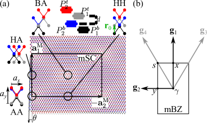
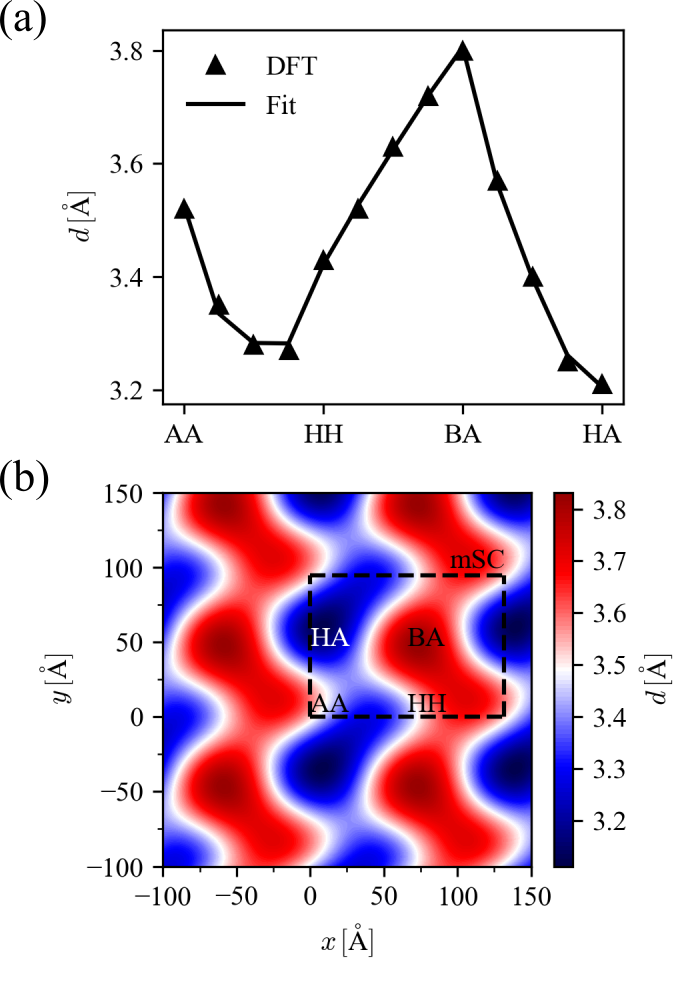
The moiré pattern formed by a twisted phosphorene bilayer with small twist angle is an approximate superlattice, as shown in Fig. 1(a). Locally, every region of its mSC approximates a commensurate stacking configuration between two perfectly aligned monolayers, each one uniquely determined by an in-plane offset vector , representing the relative displacement of the top layer with respect to the bottom one, and a local interlayer distance . Figure 1(a) shows the four most highly symmetrical stacking configurations, and illustrates the offset vector in the case of HH stacking. The values taken by for all four configurations are listed in Table 1. The interlayer distance dependence on stacking will be discussed in Secs. III and V.
| Stacking | |
|---|---|
| AA | |
| HH | |
| BA | |
| HA |
In reciprocal space, the th Bragg vector of the moiré superlattice is , where and are reciprocal lattice vectors of the rotated top- and bottom layers, respectively. In terms of the reciprocal vectors of an unrotated layer, these are given by
| (1) |
where represents rotation by angle about the axis. In this paper, we have chosen the basis Bragg vectors
| (2) |
with lattice constants and determined by ab initio calculations in Sec. III, and illustrated in Fig. 1(a). The basis moiré vectors
| (3) |
and the corresponding moiré Brillouin zone (mBZ) are shown in Fig. 1(b). The mSC vectors
| (4) |
are shown in Fig. 1(a).
In a large-periodicity moiré superlattice, where the stacking configuration varies slowly across the mSC, the low energy electronic states are well described by the so-called continuum approximation. This approach has found remarkable success in describing electrons in twisted bilayer graphene[23, 24, 25, 26] and twisted homo- and heterostructures of transition-metal dichalcogenides[27, 28, 29, 30, 31, 32, 33, 21, 22]. The approximation consists of treating as a vector field defined over the continuum of points in the sample plane. For a two-dimensional homobilayer with twist angle , is well approximated by
| (5) |
All superlattice parameters depending on , such as the interlayer distance , can then be interpolated for all values of by the substitution (5), from known values at a finite number of stacking configurations.
Here, we use this approach to interpolate an effective electronic Hamiltonian for the conduction and valence bands of twisted bilayer phosphorene. To achieve this, in Sec. III we compute the band structures of multiple aligned () phosphorene bilayers at different stacking configurations using DFT. Then, in Sec. IV we develop effective -dependent Hamiltonians for the band-edge electrons of aligned phosphorene bilayers, using a symmetry-based approach. These models are then parametrized to match the DFT results in Sec. IV.4. In Sec. V, we use Eq. (5) to interpolate the parametrized Hamiltonians across the mSC, obtaining a continuous approximation to the superlattice Hamiltonian, which we solve numerically using zone-folding methods to compute the moiré mini-band structures of twisted phosphorene bilayers at multiple twist angles.
III Ab initio results for arbitrarily stacked phosphorene bilayers
We performed DFT computations as implemented in the Vienna Ab Initio Simulation Package[35, 36, 37] using the standard generalized gradient approximation, with the Perdew-Burke-Enzerhof (PBE) parametrization[38]. The electronic states are treated with projector-augmented wave basis sets[39]. The optimized cutoff energy for the plane wave expansion was . Since we are treating the interaction between two phosphorene layers, a dispersion-corrected van der Waals scheme is necessary. Here, we used the Grimme-D3 method, in which the dispersion coefficients are adjusted to the local geometry of the system[40]. Force and energy convergence criteria were set to 0.01 and , respectively. A -centered -points mesh of is used to sample the Brillouin zone (BZ) for structural optimization. For band structure calculations, a denser -point mesh of was used. The same mesh was also used to achieve self consistency for the fixed interlayer distance calculations.
The monolayer phosphorene used to build the bilayer systems was fully optimized to obtain the lattice parameters reported in Sec. II, which are in good agreement with previous reports[41, 42]. A vacuum gap of was used in the perpendicular direction to eliminate undesirable self-interactions between the phosphorene layers with their corresponding images generated by the artificial supercell periodicity. We performed computations for the four high-symmetry stacking configurations of Table 1. In addition, we considered three intermediate configurations at , , and of the path between each two subsequent high-symmetry stackings, following the path . In total, we studied 13 differently stacked bilayer systems.
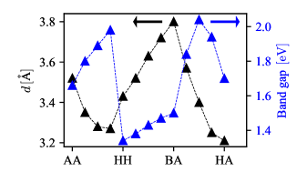
Each phosphorene monolayer is formed by two staggered P monolayers, and , separated by an interlayer distance between layers and , along the axis perpendicular to the sample plane [see Fig. 1(a)]. All models were fully optimized to obtain the interlayer distance as a function of the stacking vector . Figure 2 summarizes the main results. The shortest interlayer distance () is obtained for the HA bilayer, which constitutes the 2D building block of bulk black phosphorus[34]. HA is also the most stable configuration overall, with a lower cohesive energy than AA, BA and HH stackings by , , and , respectively. By contrast, BA bilayers are the least stable, and exhibit the largest interlayer distance overall (), due to the large repulsion between P layers and . These results are in good agreement with previous ab initio results on phosphorene bilayers[43].
It is well known[44] that, whereas DFT calculations correctly describe the band structure topology, they do not correctly reproduce the experimental band gap. To address this issue, we implement a scissor correction, following earlier studies on semiconductors[45, 46, 47, 48, 49, 50, 51], using previously reported values for HA phosphorene bilayers[34] that correctly reproduce experimental measurements,111The band gap reported in Ref. 34 is based on the DFT calculations that implement the Hartree-Fock corrected B3LYP functional. The reported band gap is . This result is consistent with the optical band gap of reported in Ref. 34, given recent calculations of -point exciton binding energies in phosphorene[63, 64]., while retaining the band gap variation as described by our DFT calculations. The scissor correction consists of a rigid translation of all conduction bands by a gap correction energy .
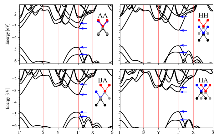
Figure 2 shows the scissor-corrected band gap variation as a function of stacking for all 13 configurations considered. All cases exhibit semiconducting behavior, with a gap energy modulation driven by the variation of the interlayer interaction strength at different interlayer distances [43]. Note that the gap energy follows the inverse trend of the interlayer distance between configurations AA and HH, when the unit cells are translated along the direction, reaching the overall minimum gap value of for HH bilayers. The band gap then grows linearly by about along the path between configurations HH and BA, following the same trend as the interlayer distance. Finally, the band varies nonmonotonically between BA and HA, reaching an overall maximum value of at the midpoint between these two configurations. Previous reports on AA, BA, HH and HA phosphorene bilayers—including the optB88-vdW functional—agree with our interlayer distances and band gap trend[43]. Our results are also consistent with data found using PBE without van der Waals interactions[53]. Calculations using the Heyd–Scuseria–Ernzerhof functional suggest that the band gaps for these stackings are approximately larger than the ones obtained by our PBE + Grimme-D3 calculations, before scissor corrections. Nonetheless, the same trend is obtained for the gap variation with stacking, showing the validity of our approximation.
Figure 3 presents detailed band structures for the four relaxed high-symmetry bilayer configurations, setting the vacuum level as a common energy reference for all cases shown. Although the four high-symmetry configurations exhibit a direct band gap at the point, analogous to the monolayer case, our DFT calculations show that four out of the nine intermediate stacking configurations deviate from this behavior, showing a valence-band maximum slightly away from along the direction, appearing approximately above the -point valence band edge and making the gap slightly indirect. Further details can be found in Appendix A. It is unclear whether these features might change in a more sophisticated ab initio scheme (e.g., ). In the following, we shall focus on the band gap at the point when describing the different stacking regions inside a mSC formed by a twisted phosphorene bilayer. This approximation is justified if one considers that, in an actual twisted bilayer, the different stacking regions will grow or shrink according to their corresponding adhesion energies, as has been consistently observed in other 2D materials, such as graphene[54, 55] and transition-metal dichalcogenides[13, 14]. In the case at hand, BA stacking regions will shrink in favor of AA, HH and especially HA regions. The latter shall grow to form domains that occupy most of the mSC area. In turn, we expect all intermediate stacking regions to become domain walls, occupying only a small area of the mSC, and becoming less important for the description of the superlattice electronic states.
IV Effective Hamiltonians for arbitrarily stacked phosphorene bilayers
IV.1 General approach
In this section we formulate effective -point Hamiltonians for the lowest two conduction- and highest two valence subbands (see Fig. 3) of an aligned phosphorene bilayer at arbitrary stacking. These models are based on same-band interlayer hybridization between monolayer states, treating interlayer conduction-valence hybridization in second-order perturbation theory, as justified by the large monolayer energy gap of at the point[34]. The resulting Hamiltonian for band for conduction and valence, respectively, takes the form
| (6) |
where the in-plane offset vector gives the specific stacking configuration.
The hopping term corresponds to the interlayer matrix element
| (7) |
of the effective microscopic Hamiltonian developed in Sec. IV.2 below, between the Bloch states and , corresponding to electrons of momentum and band index of the top- and bottom layers, respectively. Note that we have omitted the spin index for states near the point, where spin degeneracy is guaranteed. By contrast, the top- and bottom-layer state energies (with for the top and bottom layers, respectively), consists of three contributions:
| (8) |
Here, is an -independent term, containing the energy of the monolayer -band state at the point and -dependent energy corrections, where is the interlayer distance. represents the crystal potential of the layer opposite to . Finally, the correction term originates from virtual tunneling of -band electrons of layer into the nearest bands in the opposite layer, . In the case of , we shall consider only , whereas for we shall take , where is the second (monolayer) conduction band. This provides a minimal model capable of reproducing the DFT conduction- and valence subband energies, as we shall discuss in Sec. IV.4.
IV.2 Microscopic Hamiltonian
The microscopic Hamiltonian for a perfectly aligned, arbitrarily stacked phosphorene bilayer can be represented as[21, 22]
| (9) |
where is the momentum operator, is the bare electron mass, and is the crystal potential for layer centered at position , with an in-plane vector. In terms of , and . Placing the coordinate origin on the middle plane between the two layers, we can write , with the interlayer distance.
Let be the Bloch wave function for the electronic state with wave vector and band index of the isolated monolayer , defined such that
| (10) |
with the corresponding band dispersion. The matrix elements of are
| (11) |
where is the interlayer overlap matrix element
| (12) |
and is the kinetic energy interlayer matrix element
| (13) |
Writing a general eigenstate of the system in the form
| (14) |
we obtain the generalized eigenvalue problem
| (15) |
with the column vector of coefficients defined as
| (16) |
and containing all matrix elements of , except for those involving the overlap matrix . Following Ferreira et al. [21] and Magorrian et al. [22], we transform Eq. (15) into a proper Schrödinger equation by applying the unitary transformation , resulting in the effective Hamiltonian
| (17) |
where is the anti-commutator of matrices and . Since the states decay exponentially in the out-of-plane direction, away from , the matrix elements of are exponentially suppressed by the interlayer distance. This justifies treating as a perturbation, and truncating the expansion (17) at first order in . Note, however, that contains interlayer matrix elements [see Eq. (11)], which are also of order . Up to first order in , the intra- and interlayer matrix elements of are
| (18) |
One of the useful features of the above formulation for the homobilayer Hamiltonian is that all symmetry constraints are encoded in the wave functions and crystal potentials. The former may be Fourier expanded as
| (19) |
where are the bilayer Bragg vectors, the number of unit cells in the sample, and the Fourier coefficients are decaying functions of . Then, the interlayer overlap- and kinetic energy matrix elements can be written as
| (20a) | |||
| (20b) |
At this point, we introduce two approximations: first, we approximate the Fourier series (19) by its dominant terms, corresponding to the first three stars of Bragg vectors:
| (21) |
Second, we assume that the functions vary slowly with wave vector, such that for close enough to the point we may approximate . Finally, since we are concerned exclusively with wave vectors and much smaller than any reciprocal lattice vector, we may write
| (22) |
Then, Eqs. (20a) and (20b) simplify to
| (23a) | |||
| (23b) |
where we have defined
| (24) |
IV.3 Symmetry properties of the Bloch functions
As discussed by Li and Appelbaum[56], the monolayer phosphorene crystal structure is described by the point symmetry group , with modified symmetry operations and , where represents a rotation by about the axis , and is an in-plane translation by the unit cell vector . Accordingly, all -point states transform under symmetry operations like one of the group’s irreducible representations (irreps). The transformation rules are especially simple for group , which contains only one-dimensional irreps, and take the form
| (25) |
where ; is the irreducible representation of group corresponding to band ; and is the character of under the symmetry operation (see Table 2). Note that Eq. (25) applies only to states exactly at the point.
We may obtain the symmetry properties of the Fourier coefficients by inverse-Fourier transforming Eq. (19):
| (26) |
Combining Eqs. (25) and (26) for we obtain
| (27) |
where we defined and . Since in two dimensions rotations by are equivalent to in-plane inversion, Eq. (27) can be rewritten as
| (28) |
A similar analysis of the symmetry operations , and inversion yields the constraints
| (29a) | |||
| (29b) | |||
| (29c) |
respectively, with the mirror reflections and . Note that Eqs. (28) and (29a)-(29c) apply also to , appearing in .
In Appendix B, we show how Eqs. (28)–(29c) constrain the different Fourier components of the monolayer phosphorene conduction () and valence () bands, for the Bragg vectors of Eq. (21). The results are summarized in Eq. (47). Combined with (23a), (23b) and (18), these constraints give the interlayer tunneling matrix elements
| (30a) | |||
| (30b) | |||
| (30c) |
with the definitions
| (31) |
A similar analysis (see Appendix C) yields the intralayer matrix elements
| (32a) | |||
| (32b) | |||
| (32c) |
obtained from Eq. (57) by substituting .
Finally, the virtual tunneling corrections are obtained by considering first-order interlayer tunneling between band and nearby bands , as described in Sec. IV.1, and then projecting out band up to second order in perturbation theory by means of Löwdin’s partitioning method[57]. The details are discussed in Appendix D. Here, we merely state the result ():
| (33) |
Putting together Eqs. (32) and (33) and comparing with Eq. (8) gives
| (34a) | |||
| (34b) | |||
| (34c) |
This completes the derivation of all terms defining the Hamiltonian (6). Although Eqs. (30a), (30b), (32a), (32b) and (33) can ultimately be expressed in terms of microscopic quantities, our strategy will consist of fitting all parameters to first principles results, as described in Sec. IV.4 below.
IV.4 Ab initio parametrization of the effective model
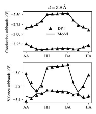
The tunneling coefficients and potential energies and appearing in Eqs. (30) and (34), respectively, were fitted to reproduce the conduction- and valence subband (see Fig. 3) energies obtained from scissor-corrected DFT calculations for multiple stacking configurations , at fixed interlayer distance . Figure 4 shows a comparison between the DFT-computed energies, and the energies obtained from the effective models (6) with parameters fitted to the DFT data, for fixed interlayer distance . The fitting procedure was repeated for and . In all cases, we found that good agreement with the DFT energies can be obtained setting . Note that suggests the absence of an out-of-plane ferroelectric effect, such as that observed in transition-metal dichalcogenide homo- and heterobilayers[58], in agreement with recent ab initio results[59].
The dependence of each remaining model parameter was then fitted as , taking as a reference interlayer distance (see Sec. V below). In the limit of , corresponding to two decoupled bilayers, all model parameters should vanish, with the exception of , which should converge to the monolayer -band edge energies, . Therefore, in the following we rewrite:
| (35) |
with the scissor-corrected DFT values and . All -dependent model parameters are summarized in Table 3.
| . | . | . | . | ||||||
| . | . | . | . | ||||||
| . | . | . | . | ||||||
| . | . | . | . | ||||||
| . | . | . | . | ||||||
| . | . | . | . | ||||||
| . | . | . | . | ||||||
| . | . | ||||||||
V Continuous model for the moiré superlattice
As described in Sec. II, the continuum approximation to the moiré superlattice Hamiltonian is obtained by substituting into Eq. (6), with the in-plane position in the moiré superlattice, measured with respect to the center of a given AA-stacked region. Note, however, that the resulting model contains the interlayer distance as a fixed parameter. To take into account out-of-plane lattice relaxation, i.e., the fact that the interlayer distance will vary across the mSC according to the local stacking, we interpolate the DFT values for the interlayer distance reported in Fig. 2 by the Fourier series
| (36) |
where the constant was chosen as a reference interlayer distance when fitting the model parameters reported in Table 3. Good agreement between (36) and the DFT results is obtained for , with the fitting parameters reported in Table 4, as shown in Fig. 5. Then, the full spatial dependence of each parameter in Table 3 takes the form
| (37) |
where we have noted that, upon the substitution ,
| (38) |
for . In practice, we utilize a first-order expansion of the exponential
| (39) |
for all conduction-band parameters, and a second-order expansion for the valence band parameters. The latter is necessary to correctly reproduce the effective gauge (moiré) potential for valence-band electrons defined by the effective model . A detailed discussion of this can be found in Appendix E.
| 1 | . | . | ||
| 2 | . | . | ||
| 3 | . | . | ||
| 4 | . | . | ||
The interpolated band Hamiltonians now explicitly contain the superlattice periodicity through the moiré Bragg vectors , and can be numerically diagonalized in a zone-folding scheme: Let be a vector of the mBZ shown in Fig. 1, and consider how acts on the monolayer plane-wave states ()
| (40) |
where are the monolayer surface areas, assumed equal. Taking the interlayer tunneling term as an example, we obtain the following matrix elements:
| (41) |
Note that these matrix elements either conserve the total wave vector by setting , or else couple states with wave vectors differing by a first- to sixth-star moiré Bragg vector, as . Similarly, for the intralayer matrix elements we have [see Eq. (34)]
| (42) |
where the first term conserves the wave vector, and the matrix elements have as similar structure to that of Eq. (41). Note that we have generalized the Bloch function energy to wave vectors close to the point as , by introducing the kinetic energy terms
| (43) |
Here, , , and are the monolayer-band effective masses[60], and the relative interlayer twist angle is included through the passive rotation of the monolayer dispersions.
The zone-folding scheme consists in mapping all states (40) lying outside the mBZ into minibands inside the mBZ as
| (44) |
labeled by the moiré vector indices . The minibands couple vertically—i.e., conserving the mBZ wave vector —amongst themselves according to the matrix elements (41) and (42), thus defining an eigenvalue problem that can be solved numerically for a finite number of minibands. In practice, we have found that the lowest conduction minibands are well converged for a range of indices , corresponding to 882 basis states, for twist angles as small as ; whereas for the valence bands a total of basis states () were needed. The resulting lowest (highest) energy eigenvalues represent the electronic energy spectra for the conduction (valence) bands around the point of the mBZ.
VI Moiré minibands in twisted phosphorene bilayers
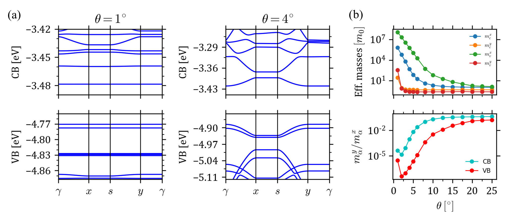
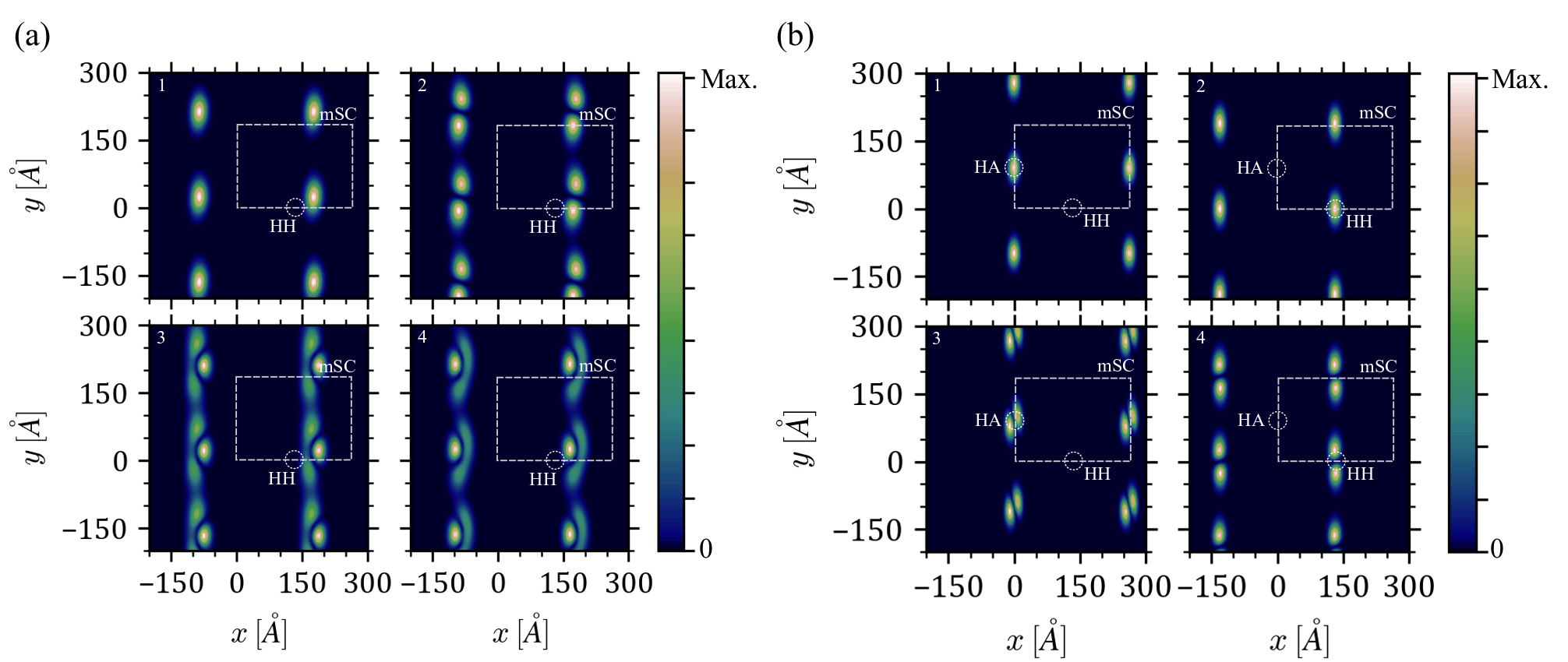
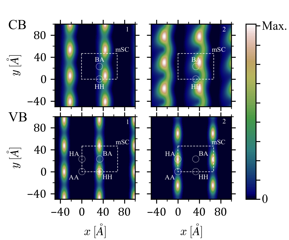
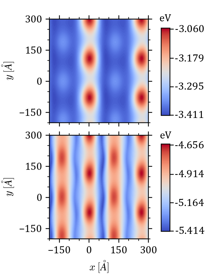
Figure 6(a) shows the first few conduction- and valence minibands for twist angles and . Flat minibands, corresponding to carrier states with vanishing group velocities, form for . To visualize the spatial distribution of the flat-miniband states, Fig. 7 shows their moduli squared averaged across the mBZ. The flat minibands correspond to arrays of spin-degenerate localized states, one per mSC, with the periodicity of the moiré superlattice. Conduction electrons localize near areas with HH stacking, whereas valence holes localize at regions of the mSC. In both cases, the localized states stretch along the axis, following the anisotropies of the corresponding moiré potentials, shown in Fig. 11 of Appendix E. Thus, the localized wavefunctions approximately inherit the symmetry of the monolayer crystals, a feature that can be identified experimentally by scanning tunneling microscopy. This is most clearly observed in the lowest-energy conduction and highest-energy valence wavefunctions, which are -like states stretched along the phosphorene unit cell’s long axis (see Fig. 1). The second-lowest conduction miniband resembles a slightly rotated orbital, whereas the third and fourth ones clearly reflect the irregularities of the electron-confining potential, in particular its lack of an mirror symmetry. In the valence case, the second-highest miniband is also formed by -like orbitals elongated in the axis, but localized at mSC regions, where a local minimum appears in the moiré potential (Fig. 11). This alternation between localization at and areas continues for the next two valence minibands, which resemble orbitals deformed by the confining potential anisotropy.
When electron-electron interactions are taken into account, the localized conduction- and valence states described above for suggest the realization of SU Hubbard model physics for both -point electrons and holes, putting twisted phosphorene bilayers in the list of twistronic Hubbard materials, together with transition-metal dichalcogenide bilayer structures[5, 6]. We shall henceforth refer to this as the Hubbard regime.
An altogether different regime is found for , where the lowest conduction- and highest valence minibands remain flat along the direction (along the segments and ), but become dispersive in the direction—a consequence of the large mass anisotropies of the monolayer bands. Figure 8 shows that these minibands correspond to arrays of quasi-one-dimensional states that propagate along the axis. For conduction electrons, these 1D states cross the HH and BA regions of the mSC, whereas valence holes exhibit a richer behavior. We find a nearly degenerate doublet of 1D states crossing the mSC at different regions: for the highest minibands, the 1D states propagate along the segment, whereas the next highest miniband corresponds to a 1D state along the line. In both cases, delocalization follows the shrinking of the mSC with increasing twist angle, which introduces a spatial overlap between neighboring localized states along the direction. We predict that these states should behave as coupled Tomonaga-Luttinger liquids[61, 62] in the presence of electron-electron interactions, and we will refer to this as the Tomonaga-Luttinger regime.
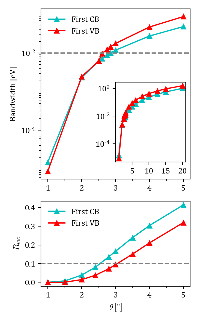
To establish the crossover between the Hubbard- an Tomonaga-Luttinger regimes, Fig. 9 shows two quantitative indicators of localization for the bottom conduction- and top valence minibands. In the top panel, we report their bandwidths for twist angles between and , where a vanishing bandwidth is characteristic of the fully localized states of the Hubbard regime, whereas the Tomonaga-Luttinger regime exhibits a finite bandwidth. Based on typical experimental resolutions, we propose a 10 meV bandwidth as a reasonable value to define the crossover between the two regimes, which occurs around for the conduction band, and around for the valence band.
A consistent result is obtained by considering the probability density ratio
| (45) |
where is the mBZ-averaged miniband wave-function squared reported in Figs. 7 and 8. The ratio (45) compares the state’s weights at two different positions in an arbitrary mSC: , which is the localization site in the Hubbard regime (near HH for the conduction miniband, and HA for the valence miniband), and , corresponding to the position half way between that site and its replica in the next mSC along the positive axis. This ratio vanishes in the Hubbard limit, and tends to 1 deep in the Tomonaga-Luttinger limit. Setting the threshold between the two regimes at , the bottom panel of Fig. 9 also establishes the crossover twist angles and for the conduction- and valence minibands, respectively.
Finally, our model predicts fully dispersive, anisotropic conduction- and valence minibands at twist angles , which we call the ballistic regime. However, as discussed in Sec. II, our continuous model represents a good approximation to the superlattice Hamiltonian only for small enough twist angles, for which the moiré periodicity is much larger than the atomic spacings. From Eq. (4) we can estimate that this condition roughly corresponds to , indicating that the crossover between the Tomonaga-Luttinger and ballistic regimes is not accurately described by our continuous model, including the specific crossover angles. Having forewarned the reader, we shall now assume that the continuous model can at least describe the ballistic regime at the qualitative level, and report our results. To quantify the anisotropies of the first conduction- and valence minibands, in Fig. 6(b) we plot their mass ratio for a wide range of twist angles. For the valence band, the mass ratio varies across three decades between and , indicating that the twist angle is an efficient knob for tuning the mass anisotropy of holes. A more modest but still quite significant variation of a factor of 10 is found for the mass ratio in the case of the lowest conduction miniband.
The continuous superlattice model predictions summarized in this section are in excellent agreement with recent results based on large-scale DFT calculations, reported in Refs. 16 and 18, with one exception: For the Tomonaga-Luttinger regime, both references identify the highest valence miniband with the 1D states propagating along the segment of the mSC, which we identify as the second highest valence miniband. We attribute this quantitative discrepancy to the similar depths of the competing potential wells for holes appearing at HA and HH regions of the superlattice, as shown in Fig. 11 of Appendix E. The energy order of the resulting states will necessarily depend on the fine quantitative details, which can differ in distinct DFT approximations.
We remark that our numerical calculations, which rely on the model parametrization presented in Table 3 and the zone-folding approach described in Sec. V, were carried out at a low computational cost, and are easily reproducible. Moreover, the moiré gauge potential picture that derives from the continuum approximation to the superlattice Hamiltonian, discussed in detail in Appendix E, provides an intuitive picture for the origin of the low-dimensional states that emerge in the Hubbard and Tomonaga-Luttinger regimes. Admittedly, the validity of our continuous model in the large twist angle- or ballistic regime is questionable due to the reduced superlattice periodicity. However, the qualitative agreement between our results and the ab initio calculations of Ref. [18] lends some credibility to our extrapolation to large twist angles.
VII Conclusions
In this paper, we have proposed a moiré superlattice Hamiltonian capable of describing the low-energy electronic spectra of twisted phosphorene bilayers. Numerical diagonalization of our model within a zone folding scheme has revealed three qualitatively distinct types of electronic states, depending on the twist angle: At small twist angles , electrons and holes localize near regions of the mSC with approximate local HH- and HA stackings, respectively, giving mesoscale realizations of the SU(2) Hubbard model on a rectangular lattice, and motivating the term Hubbard regime. At intermediate angles , we predict the formation of arrays of quasi-1D states that propagate across the mSC, along the long axis of the phosphorene unit cell. Each of these states can potentially exhibit Luttinger liquid properties, which motivates the term Tomonaga-Luttinger regime. Finally, fully dispersive minibands are recovered at large twist angles , which we call the ballistic regime. In this case, we propose the twist angle as an efficient knob for tuning the miniband anisotropies, modulating their mass ratios by up to a factor of in the conduction case, and of in the valence case. We believe that observation of these regimes is well within current experimental capabilities, by a combination of scanning tunneling microscopy and transport experiments. All of our results are in good agreement with large-scale ab initio calculations found in the recent literature[16, 18, 20]. The effective models developed in this paper are easily reproducible at a low computational cost, and motivate an intuitive understanding of the emergence of low-dimensional states based on the local properties of the different mSC regions.
To construct our superlattice Hamiltonian, we have formulated symmetry-based effective models for the lowest conduction- and highest valence -point subband states of aligned phosphorene bilayers with arbitrary stacking. These models have been parametrized based on PBE + Grimme-D3 DFT calculations, supplemented with scissor corrections for the band gap, and fully taking into account out-of-plane relaxation of the bilayer system. We propose that these models may be used in their own right to describe the band structures of HA, HH and AA bilayer phosphorene domains. Analogous to the cases of twisted bilayer graphene[54, 55] and twisted transition-metal dichalcogenide homo- and heterobilayers[13, 14], strong in-plane relaxation may also occur in twisted phosphorene bilayers at small enough twist angles, resulting in the formation of large HA domains, surrounded by smaller HH and AA ones, which can be individually described by the effective models discussed in this paper.
Acknowledgements.
I.S. acknowledges financial support from CONACyT, through a Becas Nacionales graduate scholarship. J.G-S. is thankful for the support provided by DGAPA-UNAM Project No. IA100822. F.M. acknowledges funding from DGAPA-UNAM through Grant Papiit No. IN113920. D.A.R-T. acknowledges funding from CONACyT Grants No. A1-S-14407 and No. 1564464. DFT calculations were performed at the DGCTIC-UNAM Supercomputing Center, through Project No. LANCAD-UNAM-DGCTIC-368. J.G-S. thanks A. Rodríguez-Guerrero for the technical support provided throughout the project development. Finally, D.A.R-T. would like to thank V. I. Fal’ko for useful comments during the preparation of this paper.References
- Cao et al. [2018a] Y. Cao, V. Fatemi, S. Fang, K. Watanabe, T. Taniguchi, E. Kaxiras, and P. Jarillo-Herrero, Unconventional superconductivity in magic-angle graphene superlattices, Nature 556, 43 (2018a).
- Chen et al. [2020] G. Chen, A. L. Sharpe, E. J. Fox, Y.-H. Zhang, S. Wang, L. Jiang, B. Lyu, H. Li, K. Watanabe, T. Taniguchi, et al., Tunable correlated chern insulator and ferromagnetism in a moiré superlattice, Nature 579, 56 (2020).
- Sharpe et al. [2019] A. L. Sharpe, E. J. Fox, A. W. Barnard, J. Finney, K. Watanabe, T. Taniguchi, M. Kastner, and D. Goldhaber-Gordon, Emergent ferromagnetism near three-quarters filling in twisted bilayer graphene, Science 365, 605 (2019).
- Cao et al. [2018b] Y. Cao, V. Fatemi, A. Demir, S. Fang, S. L. Tomarken, J. Y. Luo, J. D. Sanchez-Yamagishi, K. Watanabe, T. Taniguchi, E. Kaxiras, et al., Correlated insulator behaviour at half-filling in magic-angle graphene superlattices, Nature 556, 80 (2018b).
- Wang et al. [2020] L. Wang, E.-M. Shih, A. Ghiotto, L. Xian, D. A. Rhodes, C. Tan, M. Claassen, D. M. Kennes, Y. Bai, B. Kim, K. Watanabe, T. Taniguchi, X. Zhu, J. Hone, A. Rubio, A. N. Pasupathy, and C. R. Dean, Correlated electronic phases in twisted bilayer transition metal dichalcogenides, Nat. Mater. 19, 861 (2020).
- Tang et al. [2020] Y. Tang, L. Li, T. Li, Y. Xu, S. Liu, K. Barmak, K. Watanabe, T. Taniguchi, A. H. MacDonald, J. Shan, and K. F. Mak, Simulation of hubbard model physics in wse2/ws2 moirésuperlattices, Nature 579, 353 (2020).
- Jin et al. [2019] C. Jin, E. C. Regan, A. Yan, M. I. B. Utama, D. Wang, S. Zhao, Y. Qin, S. Yang, Z. Zheng, S. Shi, et al., Observation of moiré excitons in wse 2/ws 2 heterostructure superlattices, Nature 567, 76 (2019).
- Alexeev et al. [2019] E. M. Alexeev, D. A. Ruiz-Tijerina, M. Danovich, M. J. Hamer, D. J. Terry, P. K. Nayak, S. Ahn, S. Pak, J. Lee, J. I. Sohn, et al., Resonantly hybridized excitons in moiré superlattices in van der waals heterostructures, Nature 567, 81 (2019).
- Seyler et al. [2019] K. L. Seyler, P. Rivera, H. Yu, N. P. Wilson, E. L. Ray, D. G. Mandrus, J. Yan, W. Yao, and X. Xu, Signatures of moiré-trapped valley excitons in mose2/wse2 heterobilayers, Nature 567, 66 (2019).
- Tran et al. [2019] K. Tran, G. Moody, F. Wu, X. Lu, J. Choi, K. Kim, A. Rai, D. A. Sanchez, J. Quan, A. Singh, J. Embley, A. Zepeda, M. Campbell, T. Autry, T. Taniguchi, K. Watanabe, N. Lu, S. K. Banerjee, K. L. Silverman, S. Kim, E. Tutuc, L. Yang, A. H. MacDonald, and X. Li, Evidence for moiréexcitons in van der waals heterostructures, Nature 567, 71 (2019).
- Brotons-Gisbert et al. [2020] M. Brotons-Gisbert, H. Baek, A. Molina-Sánchez, A. Campbell, E. Scerri, D. White, K. Watanabe, T. Taniguchi, C. Bonato, and B. D. Gerardot, Spin–layer locking of interlayer excitons trapped in moirépotentials, Nature Materials 19, 630 (2020).
- Ruiz-Tijerina et al. [2020] D. A. Ruiz-Tijerina, I. Soltero, and F. Mireles, Theory of moiré localized excitons in transition metal dichalcogenide heterobilayers, Phys. Rev. B 102, 195403 (2020).
- Weston et al. [2020] A. Weston, Y. Zou, V. Enaldiev, A. Summerfield, N. Clark, V. Zólyomi, A. Graham, C. Yelgel, S. Magorrian, M. Zhou, J. Zultak, D. Hopkinson, A. Barinov, T. H. Bointon, A. Kretinin, N. R. Wilson, P. H. Beton, V. I. Fal’ko, S. J. Haigh, and R. Gorbachev, Atomic reconstruction in twisted bilayers of transition metal dichalcogenides, Nat. Nanotechnol. 15, 592 (2020).
- Rosenberger et al. [2020] M. R. Rosenberger, H.-J. Chuang, M. Phillips, V. P. Oleshko, K. M. McCreary, S. V. Sivaram, C. S. Hellberg, and B. T. Jonker, Twist angle-dependent atomic reconstruction and moirépatterns in transition metal dichalcogenide heterostructures, ACS Nano 14, 4550 (2020).
- Sevik et al. [2017] C. Sevik, J. R. Wallbank, O. Gülseren, F. M. Peeters, and D. Çakır, Gate induced monolayer behavior in twisted bilayer black phosphorus, 2D Mater. 4, 035025 (2017).
- Kang et al. [2017] P. Kang, W.-T. Zhang, V. Michaud-Rioux, X.-H. Kong, C. Hu, G.-H. Yu, and H. Guo, Moiré impurities in twisted bilayer black phosphorus: Effects on the carrier mobility, Phys. Rev. B 96, 195406 (2017).
- Fang et al. [2019] T. Fang, T. Liu, Z. Jiang, R. Yang, P. Servati, and G. Xia, Fabrication and the interlayer coupling effect of twisted stacked black phosphorus for optical applications, ACS Applied Nano Materials 2, 3138 (2019), https://doi.org/10.1021/acsanm.9b00462 .
- Brooks et al. [2020] J. Brooks, G. Weng, S. Taylor, and V. Vlcek, Stochastic many-body perturbation theory for moiré states in twisted bilayer phosphorene, J. Phys.: Condens. Matter 32, 234001 (2020).
- Zhao et al. [2021] S. Zhao, E. Wang, E. A. Üzer, S. Guo, R. Qi, J. Tan, K. Watanabe, T. Taniguchi, T. Nilges, P. Gao, Y. Zhang, H.-M. Cheng, B. Liu, X. Zou, and F. Wang, Anisotropic moiréoptical transitions in twisted monolayer/bilayer phosphorene heterostructures, Nat. Commun. 12, 3947 (2021).
- Wang and Zou [2022] E. Wang and X. Zou, Moiré bands in twisted trilayer black phosphorene: effects of pressure and electric field, Nanoscale 14, 3758 (2022).
- Ferreira et al. [2021] F. Ferreira, S. J. Magorrian, V. V. Enaldiev, D. A. Ruiz-Tijerina, and V. I. Fal’ko, Band energy landscapes in twisted homobilayers of transition metal dichalcogenides, Appl. Phys. Lett. 118, 241602 (2021), https://doi.org/10.1063/5.0048884 .
- Magorrian et al. [2021] S. J. Magorrian, V. V. Enaldiev, V. Zólyomi, F. Ferreira, V. I. Fal’ko, and D. A. Ruiz-Tijerina, Multifaceted moiré superlattice physics in twisted bilayers, Phys. Rev. B 104, 125440 (2021).
- Bistritzer and MacDonald [2011] R. Bistritzer and A. H. MacDonald, Moiré bands in twisted double-layer graphene, Proc. Natl. Acad. Sci. U.S.A. 108, 12233 (2011), https://www.pnas.org/content/108/30/12233.full.pdf .
- Koshino [2015] M. Koshino, Interlayer interaction in general incommensurate atomic layers, New J. Phys. 17, 015014 (2015).
- Koshino and Moon [2015] M. Koshino and P. Moon, Electronic properties of incommensurate atomic layers, J. Phys. Soc. Jpn. 84, 121001 (2015), https://doi.org/10.7566/JPSJ.84.121001 .
- Kim et al. [2017] K. Kim, A. DaSilva, S. Huang, B. Fallahazad, S. Larentis, T. Taniguchi, K. Watanabe, B. J. LeRoy, A. H. MacDonald, and E. Tutuc, Tunable moiré bands and strong correlations in small-twist-angle bilayer graphene, Proc. Natl. Acad. Sci. U.S.A. 114, 3364 (2017), https://www.pnas.org/content/114/13/3364.full.pdf .
- Yu et al. [2015] H. Yu, Y. Wang, Q. Tong, X. Xu, and W. Yao, Anomalous light cones and valley optical selection rules of interlayer excitons in twisted heterobilayers, Phys. Rev. Lett. 115, 187002 (2015).
- Wang et al. [2017] Y. Wang, Z. Wang, W. Yao, G.-B. Liu, and H. Yu, Interlayer coupling in commensurate and incommensurate bilayer structures of transition-metal dichalcogenides, Phys. Rev. B 95, 115429 (2017).
- Wu et al. [2018a] F. Wu, T. Lovorn, and A. H. MacDonald, Theory of optical absorption by interlayer excitons in transition metal dichalcogenide heterobilayers, Phys. Rev. B 97, 035306 (2018a).
- Wu et al. [2018b] F. Wu, T. Lovorn, E. Tutuc, and A. H. MacDonald, Hubbard model physics in transition metal dichalcogenide moiré bands, Phys. Rev. Lett. 121, 026402 (2018b).
- Wu et al. [2019] F. Wu, T. Lovorn, E. Tutuc, I. Martin, and A. H. MacDonald, Topological insulators in twisted transition metal dichalcogenide homobilayers, Phys. Rev. Lett. 122, 086402 (2019).
- Ruiz-Tijerina and Fal’ko [2019] D. A. Ruiz-Tijerina and V. I. Fal’ko, Interlayer hybridization and moiré superlattice minibands for electrons and excitons in heterobilayers of transition-metal dichalcogenides, Phys. Rev. B 99, 125424 (2019).
- Enaldiev et al. [2021] V. V. Enaldiev, F. Ferreira, S. J. Magorrian, and V. I. Fal’ko, Piezoelectric networks and ferroelectric domains in twistronic superlattices in WS2/MoS2 and WSe2/MoSe2 bilayers, 2D Mater. 8, 025030 (2021).
- Castellanos-Gomez et al. [2014] A. Castellanos-Gomez, L. Vicarelli, E. Prada, J. O. Island, K. L. Narasimha-Acharya, S. I. Blanter, D. J. Groenendijk, M. Buscema, G. A. Steele, J. V. Alvarez, H. W. Zandbergen, J. J. Palacios, and H. S. J. van der Zant, Isolation and characterization of few-layer black phosphorus, 2D Mater. 1, 025001 (2014).
- Kresse and Hafner [1993] G. Kresse and J. Hafner, Ab initio molecular dynamics for liquid metals, Phys. Rev. B 47, 558(R) (1993).
- Kresse and Furthmüller [1996] G. Kresse and J. Furthmüller, Efficient iterative schemes for ab initio total-energy calculations using a plane-wave basis set, Phys. Rev. B 54, 11169 (1996).
- Kresse and Furthmüller [1996] G. Kresse and J. Furthmüller, Efficiency of ab-initio total energy calculations for metals and semiconductors using a plane-wave basis set, Computational Materials Science 6, 15 (1996).
- Perdew et al. [1996] J. P. Perdew, K. Burke, and M. Ernzerhof, Generalized gradient approximation made simple, Phys. Rev. Lett. 77, 3865 (1996).
- Kresse and Joubert [1999] G. Kresse and D. Joubert, From ultrasoft pseudopotentials to the projector augmented-wave method, Phys. Rev. B 59, 1758 (1999).
- Grimme et al. [2010] S. Grimme, J. Antony, S. Ehrlich, and H. Krieg, A consistent and accurate ab initio parametrization of density functional dispersion correction (dft-d) for the 94 elements h-pu, J. Chem. Phys. 132, 154104 (2010), https://doi.org/10.1063/1.3382344 .
- Liu et al. [2014] H. Liu, A. T. Neal, Z. Zhu, Z. Luo, X. Xu, D. Tománek, and P. D. Ye, Phosphorene: An unexplored 2d semiconductor with a high hole mobility, ACS Nano 8, 4033 (2014).
- Peng et al. [2014] X. Peng, Q. Wei, and A. Copple, Strain-engineered direct-indirect band gap transition and its mechanism in two-dimensional phosphorene, Phys. Rev. B 90, 085402 (2014).
- Dai and Zeng [2014] J. Dai and X. C. Zeng, Bilayer phosphorene: Effect of stacking order on bandgap and its potential applications in thin-film solar cells, J. Phys. Chem. Lett. 5, 1289 (2014).
- Schlüter and Sham [1990] M. Schlüter and L. Sham, Density-functional theory of the band gap, in Density Functional Theory of Many-Fermion Systems, Advances in Quantum Chemistry, Vol. 21, edited by P.-O. Löwdin (Academic Press, Cambridge, Massachusetts, 1990) pp. 97–112.
- Fiorentini and Baldereschi [1995] V. Fiorentini and A. Baldereschi, Dielectric scaling of the self-energy scissor operator in semiconductors and insulators, Phys. Rev. B 51, 17196 (1995).
- Johnson and Ashcroft [1998] K. A. Johnson and N. W. Ashcroft, Corrections to density-functional theory band gaps, Phys. Rev. B 58, 15548 (1998).
- Bernstein et al. [2002] N. Bernstein, M. J. Mehl, and D. A. Papaconstantopoulos, Nonorthogonal tight-binding model for germanium, Phys. Rev. B 66, 075212 (2002).
- Parashari et al. [2008] S. S. Parashari, S. Kumar, and S. Auluck, Calculated structural, electronic and optical properties of ga-based semiconductors under pressure, Physica B: Condensed Matter 403, 3077 (2008).
- Thilagam et al. [2010] A. Thilagam, D. J. Simpson, and A. R. Gerson, A first-principles study of the dielectric properties of TiO2polymorphs, J. Phys.: Condens. Mat. 23, 025901 (2010).
- Ramesh Babu et al. [2011] K. Ramesh Babu, C. Bheema Lingam, S. Auluck, S. P. Tewari, and G. Vaitheeswaran, Structural, thermodynamic and optical properties of mgf2 studied from first-principles theory, J. Solid State Chem. 184, 343 (2011).
- Magorrian et al. [2016] S. J. Magorrian, V. Zólyomi, and V. I. Fal’ko, Electronic and optical properties of two-dimensional inse from a dft-parametrized tight-binding model, Phys. Rev. B 94, 245431 (2016).
- Note [1] The band gap reported in Ref. \rev@citealpCastellanos_Gomez_2014 is based on the DFT calculations that implement the Hartree-Fock corrected B3LYP functional. The reported band gap is . This result is consistent with the optical band gap of reported in Ref. \rev@citealpCastellanos_Gomez_2014, given recent calculations of -point exciton binding energies in phosphorene[63, 64].
- Zhang et al. [2015] T. Zhang, J.-H. Lin, Y.-M. Yu, X.-R. Chen, and W.-M. Liu, Stacked bilayer phosphorene: strain-induced quantum spin hall state and optical measurement, Sci. Rep. 5, 13927 (2015).
- Zhang and Tadmor [2018] K. Zhang and E. B. Tadmor, Structural and electron diffraction scaling of twisted graphene bilayers, J. Mech. Phys. Solids 112, 225 (2018).
- Yoo et al. [2019] H. Yoo, R. Engelke, S. Carr, S. Fang, K. Zhang, P. Cazeaux, S. H. Sung, R. Hovden, A. W. Tsen, T. Taniguchi, K. Watanabe, G.-C. Yi, M. Kim, M. Luskin, E. B. Tadmor, E. Kaxiras, and P. Kim, Atomic and electronic reconstruction at the van der waals interface in twisted bilayer graphene, Nat. Mater. 18, 448 (2019).
- Li and Appelbaum [2014] P. Li and I. Appelbaum, Electrons and holes in phosphorene, Phys. Rev. B 90, 115439 (2014).
- Winkler [2003] R. Winkler, Spin-orbit coupling effects in two-dimensional electron and hole systems, Springer Tracts in Modern Physics No. 191 (Springer-Verlag Berlin Heidelberg, 2003).
- Weston et al. [2022] A. Weston, E. G. Castanon, V. Enaldiev, F. Ferreira, S. Bhattacharjee, S. Xu, H. Corte-León, Z. Wu, N. Clark, A. Summerfield, T. Hashimoto, Y. Gao, W. Wang, M. Hamer, H. Read, L. Fumagalli, A. V. Kretinin, S. J. Haigh, O. Kazakova, A. K. Geim, V. I. Fal’ko, and R. Gorbachev, Interfacial ferroelectricity in marginally twisted 2d semiconductors, Nat. Nanotechnol. 17, 390 (2022).
- Liu et al. [2020] N. Liu, J. Zhang, S. Zhou, and J. Zhao, Tuning the electronic properties of bilayer black phosphorene with the twist angle, J. Mater. Chem. C 8, 6264 (2020).
- Choi et al. [2015] J.-H. Choi, P. Cui, H. Lan, and Z. Zhang, Linear scaling of the exciton binding energy versus the band gap of two-dimensional materials, Phys. Rev. Lett. 115, 066403 (2015).
- Tomonaga [1950] S.-i. Tomonaga, Remarks on Bloch’s Method of Sound Waves applied to Many-Fermion Problems, Progress of Theoretical Physics 5, 544 (1950), https://academic.oup.com/ptp/article-pdf/5/4/544/5430161/5-4-544.pdf .
- Luttinger [1963] J. M. Luttinger, An exactly soluble model of a many‐fermion system, Journal of Mathematical Physics 4, 1154 (1963), https://doi.org/10.1063/1.1704046 .
- Faria Junior et al. [2019] P. E. Faria Junior, M. Kurpas, M. Gmitra, and J. Fabian, theory for phosphorene: Effective -factors, landau levels, and excitons, Phys. Rev. B 100, 115203 (2019).
- Henriques and Peres [2020] J. C. G. Henriques and N. M. R. Peres, Excitons in phosphorene: A semi-analytical perturbative approach, Phys. Rev. B 101, 035406 (2020).
- Niu et al. [2017] Q. Niu, M.-C. Chang, B. Wu, D. Xiao, and R. Cheng, Physical Effects of Geometric Phases (World Scientific, Singapore, 2017).
Appendix A DFT band structures for intermediate configurations
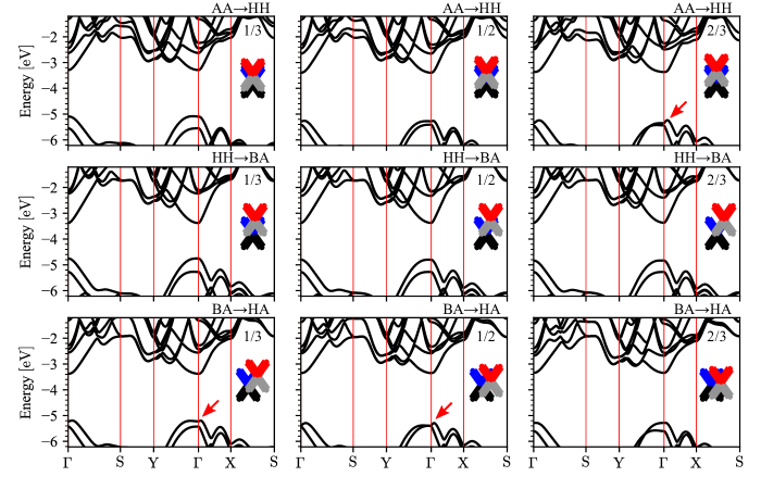
Figure 10 shows the band structures for intermediate configurations to the high-symmetry stackings listed in Table 1, following the path for values. These band structures, like those reported in Fig. 3, were obtained from PBE + Grimme-D3 DFT calculations, with a scissor-corrected band gap based on Ref. [34]. By contrast to the high-symmetry stacking cases, we find five intermediate configurations where the band gap becomes slightly indirect, due to the appearance of a global valence band maximum close to the point, along the line of the BZ. In three out of these five cases this maximum is significantly higher in energy than the -point valence state, reaching a maximum energy difference of .
Appendix B Symmetry constraints for the Fourier components of the valence- and conduction band Bloch functions
Appendix C Matrix elements of the crystal potential
As shown in Eq. (18), the intralayer matrix elements of the effective Hamiltonian for layer correspond to those of the crystal potential of the opposite layer, , given by
| (48) |
where we have Fourier expanded the crystal potential as
| (49) |
and used . Once again, we consider only and close to the point, and the momentum conservation condition simplifies to
The only non vanishing matrix elements are then
| (50) |
At this point we approximate the Bloch functions and the potential by their first few Fourier components, taking only the first three stars of Bragg vectors. In addition, we shall focus on the case , since intralayer-interband transitions are strongly suppressed by the band gap. We split Eq. (50) into the following contributions: When or with , we get
| (51) |
which is independent of stacking. Then, we consider with , and with , which give
| (52) |
where using the conditions , required for a real-valued crystal potential, and , required by rectangular symmetry, we have concluded that . Simplifying (52) and using the symmetry constraints (47), we obtain for the conduction subbands
| (53) |
having made use of the symmetry property of the potential , which gives . By contrast, for the valence subbands this contribution vanished identically, due to the fact that .
Finally, we consider the case when with , which gives
| (54) |
In this last case, we must restrict ourselves to combinations such that belongs to one of the first three stars of Bragg vectors, since we have assumed that is negligible otherwise. Every combination meets this requirement, giving a contribution which is independent of stacking, and can thus be grouped together with . The remaining possible combinations are listed in Table 5.
Appendix D Virtual tunneling corrections and Löwdin partitioning
Here, we shall consider tunneling matrix elements between the Bloch state in layer , and in the opposite layer. For , we consider only , which gives
| (58) |
For , we consider , and obtain
| (59) |
In both cases, we have the definition
| (60) |
The matrix elements (59) have the same form for either , as well as the same form as those of Eqs. (58), because all cases involve tunneling between a band that transforms like representation of group (band ), and another that transforms like representation (bands and ).
The total Hamiltonian, involving two layers with three bands each, takes the form
| (61) |
with the basis ordering . In Eq. (61), we have introduced the energy of the monolayer -point state of band , , and the tunneling matrix element , which has the same form as Eq. (30a).
Next, we project out the block up to second order in perturbation theory using Löwdin’s partitioning[57], resulting in
| (62) |
and an independent Hamiltonian for the band sector, which is not of interest to us at the moment. Repeating the projection procedure, this time to eliminate the interlayer coupling between conduction and valence bands at second order in perturbation theory, we obtain
| (63a) | |||
| (63b) |
where we have approximated
| (64) |
Expanding, e.g., , we obtain
| (65) |
and has the same form, simply exchanging everywhere in (65).
Appendix E Effective moiré gauge potentials
The effective Hamiltonians , obtained by substituting into Eq. (6), constitute effective gauge potentials[65, 21] for the phosphorene electronic states. In the limit of an infinite superlattice periodicity, the motion of an -band electron can be described by , where the position is replaced by a parameter that varies adiabatically as different regions of the twisted homobilayer are explored. From this point of view, we may compute the energy eigenvalues of as functions of the adiabatic parameter in the form
| (68) |
By reinstating , the eigenvalues and can be interpreted as effective moiré potentials acting on the conduction and valence electrons, respectively. These potentials are plotted in Fig. 11 for a twisted phosphorene bilayer.
The potential features wells capable of confining conduction electrons, shown in dark blue in the top panel of Fig. 11. These potential wells produce either the localized, quantum-dot-like states shown in Fig. 7, or the quasi-1D states shown in Fig. 8, depending on the size of the mSC, as determined by the twist angle. Similarly, shows potential barriers, depicted in the bottom panel of Fig. 11 as dark red spots, which can localize holes. Note that in the valence, in addition to the absolute minima that appear at HA regions of the mSC, there are secondary, local minima at AA stacking regions. The appearance of these two competing sets of minima made it necessary to expand the exponential functions describing the dependence of the valence-band parameters up to second order, to correctly capture the relative depths of these potential wells. Note that for both the conduction and valence cases, the potential wells are both anisotropic and irregular, explaining the asymmetric shapes of the charge densities reported in Fig. 7.