A new type of cyclotron resonance from charge-impurity scattering in the bulk-insulating Bi2Se3 thin films
Abstract
This work focuses on the low frequency Drude response of bulk-insulating topological insulator Bi2Se3 films. The frequency and field dependence of the mobility and carrier density are measured simultaneously via time-domain terahertz spectroscopy. These films are grown on buffer layers, capped by Se, and have been exposed in air for months. Under a magnetic field up to 7 Tesla, we observe prominent cyclotron resonances (CRs). We attribute the sharp CR to two different topological surface states (TSSs) from both surfaces of the films. The CR sharpens at high fields due to an electron-impurity scattering. By using magneto-terahertz spectroscopy, we confirm that these films are bulk-insulating, which paves the way to use intrinsic topological insulators without bulk carriers for applications including topological spintronics and quantum computing.
Introduction
Ordered states of matter are usually characterized by Landau’s spontaneous symmetry breaking theory. For example, ferromagnets break continuous rotation symmetry and superconductors break gauge symmetry. The newly discovered topological materials are classified by the topological properties of their bulk wavefunction. For example,the three-dimensional topological insulators (TIs) possess insulating bulk states and conducting surface states. Hasan and Kane (2010); Qi and Zhang (2011) . Intrinsic bulk-insulating TIs are the ideal platforms for low-dissipation spintronics and quantum computing due to the spin-momentum locking on the topological surface states (TSSs) Hasan and Kane (2010); Qi and Zhang (2011). However, most TI materials are slightly doped and thus have a conducting bulk, which is the major obstacle to reach the ideal TI state. To solve the problem, many attempts are made to tune the chemical potential towards the Dirac point. It was a success in graphene to probe many-body interactions with plasmons and phonons Basov et al. (2014), and in Cu doped Bi2Se3 with dominating electron-phonon couplingWu et al. (2015). More advancements in TIs are still lacking .
Bi2Se3 is a typical 3D TI with a single Dirac cone on the surface. However, native grown Bi2Se3 is known with a conducting bulk from defects. One way to suppress the bulk carrier density is the chemical doping method Ren et al. (2010); Xiong et al. (2012). However, the bulk carrier densities in these samples are still not negligible and the impurity states are pinned close to the chemical potential. The other way to suppress the bulk carriers is to grow Bi2Se3 on a buffer layer Koirala et al. (2015); Wu et al. (2016). An open question remains on how to keep the sample bulk-insulating after exposure in air. In this work, we investigate Bi2Se3 thin films grown on a buffer layer with Se capping. The TSSs are decoupled via time-domain terahertz spectroscopy with a magnetic field up to 7 tesla.
Cyclotron resonance (CR) measurements have been shown very useful to study the Dirac fermions and many-body interactions Crassee et al. (2010); Jiang et al. (2007a); Jenkins et al. (2013). It is also one of the most precise method to determine the carrier effective mass Kono and Miura (2006). In previous work, Bi2Se3 films with conducting bulk showed a large Kerr rotation without obvious resonance Valdés Aguilar et al. (2012). In a later report, CR emerges in In2Se3 capped Bi2Se3 films Jenkins et al. (2013) due to the destroyed non-TI/TI interface from Indium diffusionLee et al. (2014). This is because a phase transition from topological to trivial insulator occurs at a low Indium concentration () Wu et al. (2013). Besides, Cu doped Bi2Se3 films also presents CR, where the bulk-insulating state is reached and the electron-phonon coupling was revealed Wu et al. (2015).
Results and Discussion
Here we report time-domain THz spectroscopy measurement on Bi2Se3 thin films with 100 nm Se capping layer and (Bi1-xInx)2Se3 buffer layer (BIS-BL) Koirala et al. (2015). These films have been exposed in air for 6 months. By using cyclotron resonance measurement, we confirm that these films are still bulk-insulating. We attribute the conducting channels to two different topological surface states (TSSs) on the top and bottom of the films. By using magneto-terahertz spectroscopy, we observe that the cyclotron resonance sharpens at higher magnetic field, which reveal with long-range electron impurity scattering on the surfaces.
.
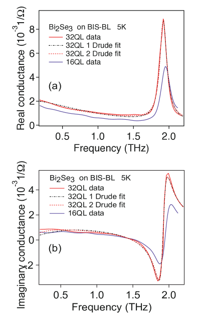
Fig.1(a)(b) shows the real and imaginary conductance for 32QL and 16QL Bi2Se3 grown on BIS-BL at 5 K. The spectral weight is lower compared with the normal Bi2Se3 directly grown on sapphire or Si Valdés Aguilar et al. (2012), even lower than the bulk-insulating Cu0.02Bi2Se3 Wu et al. (2015). This indicates the bulk insulating behavior of the samples. The spectra can be fitted by the sum of (i) two Drude terms describing free electron-like motions from top and bottom surfaces respectively, (ii) a Drude-Lorentz term describing phonon oscillations, and (iii) a constant term counting for the background above the measured spectral range, as shown below.
| (1) |
Here and are the scattering rates and plasma frequencies of the -th Drude term. and are the scattering rate and plasma frequency of the Drude-Lorentz term. is the film thickness. is a constant named lattice polarizability. In the real part of the conductance , the total spectral weight () can be extracted from the integral of each feature with a coefficient . This gives the ratio of the carrier density and the effective transport mass.
| (2) |
In the second equality, and are the carrier densities and the effective transport masses of the massless Dirac fermion. is defined as Consider a quadratic dispersion model for the TSS, , the coefficients and can be obtained from photo-emission Wu et al. (2015). Then the last term in Eq.2 can be expressed by only. For one surface state, the relation between spectral weight and is as following. Note that the right side of following expression is half of the value in the Bi2Se3 when we assume two nominally same TSSs were observed in Bi2Se3.
| (3) |
At first, a single conduction channel originated from two identical TSSs is assumed. Using Eq.2 and 3, the and m∗ can be determined. The fitting results of the 32QL sample gives a total sheet carrier density 4.8 1012/cm2, effective transport mass 0.135 (0.005) , Fermi energy E 140 (10) meV, and phonon frequency THz. 16QL sample has lower spectral weight than 32QL sample. The same analysis gives a total sheet carrier density 3.8 1012/cm2, 0.12 (0.005) , E 120 (8) meV and phonon frequency THz. The estimation of the chemical potential is consistent with an insulating bulk even after exposure in air for 6 months Koirala et al. (2015).
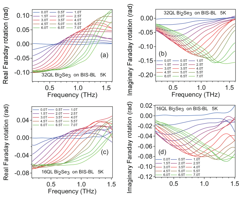
We performed Faraday rotation measurements on these samples to measure the cyclotron resonance mass and spectral weight. Data are shown in Fig.2(a)(b)(c)(d). Similar to Cu0.02Bi2Se3, cyclotron resonates are observed in both 32QL and 16QL samples. We use the following model to fit the conductance spectra under an external magnetic field. Here we assume two equal contribution from top and bottom surface states:
| (4) |
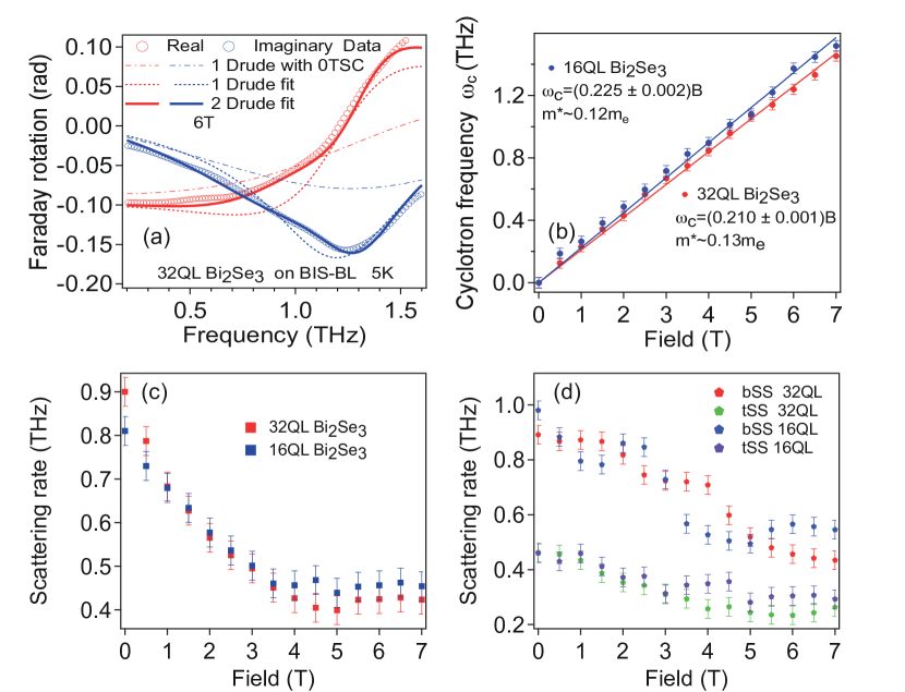
Here the sign corresponds to the right/left-hand circularly polarized light, respectively. is the CR frequency. The Faraday rotation can be expressed by . Here we let and vary with field. We find that the fit result is not good as shown in Fig. 3(a). Let us further address the 1 Drude model analysis. As we can see in Fig.3(a), the fit quality of 1 Drude term is not as good as Cu0.02Bi2Se3 case. Bi2Se3 is grown (Bi1-xInx)2Se3 and 0.2 In is diffused into the bottom Bi2Se3 few layers. Even though 0.2 is far below the topological phase transition thresholdWu et al. (2013), it is natural to treat top surface states (tSS) and bottom surface states (bSS) differently. We remove the equal contribution from both surface states and treat them separately as equation 4. The fit quality improve significantly as shown in Fig.3(a). We can also see two Drude terms fit zero-field conductance better in Fig.1. Then we can extract carrier density of each surface state by the relation . The parameters for 2 Drude fits are showed in table1. Indium causes more scattering and therefore the channel with larger scattering rate is identified as bottom surface state. As shown in previous works, the bottom surface has more defects, which lead to higher carrier density Valdés Aguilar et al. (2012); Koirala et al. (2015). Therefore, the large scattering rate and the large carrier density are consistent with each other for the bottom surface. We also performed Faraday rotation measurements on bare buffer layer and no rotation angle is observed. So the cyclotron resonance feature comes from the Bi2Se3 sample only.
| n2D (1012/cm2) | m∗ (me) | (7T) (THz) | (7T) (cm2/Vs) | |
|---|---|---|---|---|
| tSS 32QL | 2.2 | 0.13 | 0.24 | 8980 |
| bSS 32QL | 2.7 | 0.14 | 0.55 | 3640 |
| tSS 16QL | 1.3 | 0.11 | 0.29 | 8780 |
| bSS 16QL | 2.0 | 0.12 | 0.43 | 5420 |
Now let us address the decreasing scattering rate VS field as shown in Fig. 3(c-d). Short-range charge impurity scattering rate leads to increasing scattering rate, as predicted and observed in grapheneShon and Ando (1998); Orlita et al. (2008); Jiang et al. (2007b). Electron-phonon scattering rate causes broadening of cyclotron resonance and saturation of scattering rate above phonon energyWu et al. (2015). Long-range charge impurity scattering rate leads to decreasing scattering rate VS fieldYang et al. (2010). It was not the dominant mechanism in graphene and therefore was never observed. Similar trend were reported in InSe quantum well and was interpreted as scattering over Gaussian potential larger or equal to the cyclotron orbitKress-Rogers et al. (1983). The saturation of scattering rate above 4T in Fig. 3(c-d) is due to electron-phonon scattering as cyclotron frequency reaches 0.7 THz at 4 T in both samples which corresponds to either Kohn anomaly of surface phonon or highest acoustic phonon frequencyWu et al. (2015). In the two-Drude fit, one channel has stronger field dependence and is identified as bottom surface state. The reason is charge impurities most likely are created on the bottom surface state due to charge imhomogenity. Top surface state has less effect due to screening. This kind of long-range charge impurity scattering was further corroborated by the fact no Shubnikov de-Has (SdH) oscillation was observed on these sample while CR is very robustKoirala et al. (2015). SdH is limited by quantum life-time which is sensitive to both small-angle and large-angle scatting while CR is sensitive to transport life-time which is limited by back scattering. The low quantum life-time in these samples indicates significant small-angle scattering rate coming from long-range coulomb potential. Similar trend was observed in 2DEG systemGaska et al. (1998) and theoretically investigated in literatureAdam et al. (2012).
To conclude, we observe sharp cyclotron resonance in bulk-insulating Bi2Se3 thin films. The field dependence reveals a decreasing of the scattering rate with increasing magnetic fields. We attribute the origin to impurity scattering due to the buffer layer. This work shows that cyclotron resonance is a powerful tool to study many-body interactions in topological materials. On the practical side, this work establishes that a 100 nm thick Se capping layer is simple, but very useful for keeping the topological insulator thin films bulk-insulating. The evidence for the long-range impurity scattering at the bottom interface due to buffer layers shreds light on film growth to further decreases the carrier concentration and enhances mobility for future low-dissipation spintronic devices.
Acknowledgement
This project is supported from the ARO under the Grant W911NF2020166. The development of the THz polarity is supported by the ARO YIP award under the Grant W911NF1910342. The acquisition of the laser for the THz system is support from a seed grant at National Science Foundation supported University of Pennsylvania Materials Research Science and Engineering Center (MRSEC)(DMR-1720530). X.H. is also partially supported by the Gordon and Betty Moore Foundation’s EPiQS Initiative, Grant GBMF9212 to L.W . L.W. also acknowledges partial summer support from the NSF EArly-concept Grants for Exploratory Research (EAGER) grant (Grant No. DMR2132591).
Data Availability Statement
The data that support the findings of this study are all present in this paper. Further data are available from the corresponding author upon reasonable request.
References
- Hasan and Kane (2010) M. Z. Hasan and C. L. Kane, Rev. Mod. Phys. 82, 3045 (2010).
- Qi and Zhang (2011) X.-L. Qi and S.-C. Zhang, Rev. Mod. Phys. 83, 1057 (2011).
- Basov et al. (2014) D. Basov, M. Fogler, A. Lanzara, F. Wang, and Y. Zhang, Reviews of Modern Physics 86, 959 (2014).
- Wu et al. (2015) L. Wu, W.-K. Tse, M. Brahlek, C. M. Morris, R. V. Aguilar, N. Koirala, S. Oh, and N. P. Armitage, Physical Review Letters 115, 217602 (2015).
- Ren et al. (2010) Z. Ren, A. A. Taskin, S. Sasaki, K. Segawa, and Y. Ando, Phys. Rev. B 82, 241306 (2010).
- Xiong et al. (2012) J. Xiong, A. Petersen, D. Qu, Y. Hor, R. Cava, and N. Ong, Physica E 44, 917 (2012).
- Koirala et al. (2015) N. Koirala, M. Brahlek, M. Salehi, L. Wu, J. Dai, J. Waugh, T. Nummy, M.-G. Han, J. Moon, Y. Zhu, et al., Nano Letters 15, 8245 (2015).
- Wu et al. (2016) L. Wu, M. Salehi, N. Koirala, J. Moon, S. Oh, and N. Armitage, Science 354, 1124 (2016).
- Crassee et al. (2010) I. Crassee, J. Levallois, A. Walter, M. Ostler, A. Bostwick, E. Rotenberg, T. Seyller, D. Van Der Marel, and A. Kuzmenko, Nature Physics 7, 48 (2010).
- Jiang et al. (2007a) Z. Jiang, E. Henriksen, L. Tung, Y.-J. Wang, M. Schwartz, M. Han, P. Kim, and H. Stormer, Phys. Rev. Lett. 98, 197403 (2007a).
- Jenkins et al. (2013) G. S. Jenkins, D. C. Schmadel, A. B. Sushkov, H. D. Drew, M. Bichler, G. Koblmueller, M. Brahlek, N. Bansal, and S. Oh, Phys. Rev. B 87, 155126 (2013).
- Kono and Miura (2006) J. Kono and N. Miura, High Magnetic Fields: Science and Technology, Volume III, World Scientific, Singapore (2006).
- Valdés Aguilar et al. (2012) R. Valdés Aguilar, A. V. Stier, W. Liu, L. S. Bilbro, D. K. George, N. Bansal, L. Wu, J. Cerne, A. G. Markelz, S. Oh, et al., Phys. Rev. Lett. 108, 087403 (2012).
- Lee et al. (2014) H. Lee, C. Xu, S. Shubeita, M. Brahlek, N. Koirala, S. Oh, and T. Gustafsson, Thin Solid Films 556, 322 (2014).
- Wu et al. (2013) L. Wu, M. Brahlek, R. V. Aguilar, A. V. Stier, C. M. Morris, Y. Lubashevsky, L. S. Bilbro, N. Bansal, S. Oh, and N. P. Armitage, Nature Physics 9, 410 (2013).
- Shon and Ando (1998) N. H. Shon and T. Ando, Journal of the Physical Society of Japan 67, 2421 (1998).
- Orlita et al. (2008) M. Orlita, C. Faugeras, P. Plochocka, P. Neugebauer, G. Martinez, D. K. Maude, A.-L. Barra, M. Sprinkle, C. Berger, W. A. De Heer, et al., Physical review letters 101, 267601 (2008).
- Jiang et al. (2007b) Z. Jiang, E. Henriksen, L. Tung, Y.-J. Wang, M. Schwartz, M. Han, P. Kim, and H. Stormer, Physical review letters 98, 197403 (2007b).
- Yang et al. (2010) C. Yang, F. Peeters, and W. Xu, Physical Review B 82, 075401 (2010).
- Kress-Rogers et al. (1983) E. Kress-Rogers, R. Nicholas, and A. Chevy, Journal of Physics C: Solid State Physics 16, 2439 (1983).
- Gaska et al. (1998) R. Gaska, J. Yang, A. Osinsky, Q. Chen, M. A. Khan, A. Orlov, G. Snider, and M. Shur, applied physics letters 72, 707 (1998).
- Adam et al. (2012) S. Adam, E. Hwang, and S. D. Sarma, Physical Review B 85, 235413 (2012).