Fabrication of high-quality PMMA/SiOx spaced planar microcavities for strong coupling of light with monolayer WS2 excitons
Abstract
Exciton polaritons in atomically-thin transition metal dichalcogenide crystals (monolayer TMDCs) have emerged as a promising candidate to enable topological transport, ultra-efficient laser technologies, and collective quantum phenomena such as polariton condensation and superfluidity at room temperature. However, integrating monolayer TMDCs into high-quality planar microcavities to achieve the required strong coupling between the cavity photons and the TMDC excitons (bound electron-hole pairs) has proven challenging. Previous approaches to integration had to compromise between various adverse effects on the strength of light-matter interactions in the monolayer, the cavity photon lifetime, and the lateral size of the microcavity. Here, we demonstrate a scalable approach to fabricating high-quality planar microcavities with an integrated monolayer WS2 layer-by-layer by using polymethyl methacrylate/silicon oxide (PMMA/SiOx) as a cavity spacer. Because the exciton oscillator strength is well protected against the required processing steps by the PMMA layer, the microcavities investigated in this work, which have quality factors of above , can operate in the strong light-matter coupling regime at room temperature. This is an important step towards fabricating wafer-scale and patterned microcavities for engineering the exciton-polariton potential landscape, which is essential for enabling many proposed technologies.
Planar microcavities with embedded exciton-hosting materials based on the design of vertical-cavity surface-emitting lasers (VCSELs) have enabled the regime of strong light-matter coupling between excitons and photons [1]. The formation of exciton polaritons (polaritons herein), part-light part-matter bosonic quasiparticles, in these semiconductor microcavities has triggered significant research efforts, which led to the creation of Bose-Einstein condensates (BEC) [2] and superfluids [3], the demonstration of non-Hermitian effects [4], the development of electrically-driven ultra-efficient lasers [5] and the realisation of topological edge transport [6] on microchips. By using semiconductors with large exciton binding energies, some of these observations were successfully realised at room temperature [7, 8, 9, 10, 11, 12, 13, 14].
A promising family of inorganic semiconductors for future polaritonic devices are atomically-thin TMDCs [15, 16, 17, 18, 19]. However, integrating these monolayers into planar microcavities to create polaritons has turned out to be challenging because they are extremely fragile and easily damaged by various fabrication techniques [20]. Many attempts at TMDC integration by using metallic top mirrors [21, 19] or depositing the top structures directly on top of the monolayer with aggressive material deposition techniques [16, 22], have led to dramatic degradation of the photon lifetimes, exciton quantum yields, or exciton-photon coupling strengths. These properties are significantly improved by recent techniques for integrating TMDCs into all-dielectric microcavities. However, these approaches are based on micrometer-sized distributed Bragg reflector (DBR) chips [23, 24, 25, 26, 27] or mechanically exfoliated hexagonal Boron Nitride (hBN) crystals [28, 29], which massively limit its technological scalability. While all of these approaches have enabled the demonstration of many striking effects of TMDC polaritons [16, 18], which include signatures of bosonic condensation [30, 26], the spin-valley Hall effect [23], and ballistic propagation at room temperature [25], fabrication recipes which allow for both scalability and high performance of the final device to enable future TMDC polariton based technologies are still to be developed.
In this work, we introduce a method for integrating monolayer WS2 into high-quality planar microcavities with the lateral size mainly limited by the size of the monolayer. In particular, we layer PMMA/SiOx on top of the monolayer before depositing the top DBR via plasma enhanced chemical vapour deposition (PECVD). This is in contrast to using metal as the top mirror of the cavity as was done for the heavily investigated DBR/metal cavities [21, 31, 32, 19, 33, 34]. We study the effects of each processing step on the optical properties of the WS2 monolayer showing that the exciton oscillator strength is well preserved inside these structures, which enables strong light-matter coupling at room temperature. Finally, we demonstrate that the quality factors (Q-factors) of these microcavities can reach values on the order of , therefore exceeding the Q-factors of DBR/metal cavities by orders of magnitude [21, 31, 32, 34] (see Supplementary Table S1). TMDC based microcavities with comparable Q-factors were previously only realised on microchips by using the technologies that inherently limit the lateral size of the devices [28, 23, 24, 25] or dramatically strain the monolayer [35, 29].
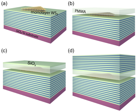
The fabrication procedure for the PMMA/SiOx spaced planar microcavities tested and discussed in this work is schematically demonstrated in Fig. 1a-d. The TiO2/SiO2 DBR substrate, which consists of 17.5 mirror pairs, is fabricated via sputtering [36] and finishes with a SiO2 capping layer that has a thickness corresponding to half of the cavity spacer. After transferring the monolayer onto the substrate (see Fig. 1a), a PMMA layer is spin-coated on top, which acts both as a protection layer and a cavity spacer (see Fig. 1b). The remaining part of the cavity-spacer (SiOx) and the top DBR (SiNx/SiOx), starting with the SiNx layer, are deposited via PECVD at 150 ∘C to finalise the microcavity (see Fig. 1c-d and Supplementary Section S2 for details). The SiOx spacer allows us to fine-tune the cavity energy and also prevents cracking of the top DBR, which we found to occur when directly depositing it onto PMMA. Most effective confinement of photons with the wavelength is achieved when the total cavity spacer and each DBR layer have a thickness of and , respectively, where is the respective refractive index of each layer [37]. In principle, the DBR substrate can be fabricated with any deposition technique suitable for making highly reflective DBRs with a smooth, high-quality layer finish.
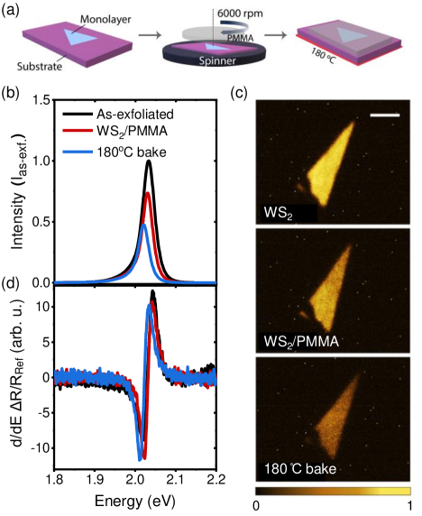
To understand the effect of PMMA deposition on the optical properties of monolayer WS2 (see Fig. 1b), we mechanically exfoliated a monolayer (bulk crystals sourced from HQ Graphene [38]) on commercial SiO2/Si substrates (sourced from Nova materials [39]). A layer PMMA (molecular weight 950,000 g/mol dissolved in anhydrous anisole with a 2.2% concentration) was then spin-coated on top of the monolayer at 6000 rpm for 60 s (see Fig. 2a). To fully remove the anisole residues and ensure a high-quality surface finish, the PMMA was hard baked at 180 ∘C for 90 s [21].
The tests of the optical response of the WS2 excitons were performed via real-space photoluminescence (PL) and white-light reflectivity measurements under ambient conditions. For the PL studies, we excited the samples with a large Gaussian spot () from a frequency doubled ND:YAG continuous wave (cw) 532-nm laser source with the excitation energy (E 2.33 eV [40]) above the A-valley exciton energy of monolayer WS2 [41]. The reflectivity spectra were measured under illumination of the sample surface with a tungsten halogen white light source. The PL spectra were obtained by averaging the signal from a small sample area, and the derivative of the reflectance contrast spectra was derived by also measuring the white light reflection next to the monolayer as reference , with . Since the product of linewidth and amplitude of the reflectance contrast spectrum at the excitonic resonance scales with the exciton oscillator strength, it quantifies the light-matter interaction in the monolayer [42, 18] required for the strong exciton-photon coupling regime.
The PL spectra in Fig. 2b show the PL quenching after the capping of monolayer WS2 with PMMA, and further degradation after baking it. This change is also seen in the corresponding PL maps (see Fig. 2c). The pronounced PL quenching effect is possibly due to the chemical instability of this material. WS2 crystals are normally n-type semiconductors due to the presence of sulphur vacancies [43, 44, 45, 46], and therefore, they can be strongly affected by the surrounding molecules [47], such as organic and water molecules that can act as dopants [48]. As a consequence, the PMMA capping process can modify the doping level of the monolayer effectively causing a reduction of the exciton quantum yield [47]. The additional decrease of the exciton PL after the baking process is likely caused by the elevated temperature accelerating the aging process (oxidation) of the monolayer, which further decreases the exciton quantum yield [49]. However, the derivative of the reflectance contrast spectra in Fig. 2d reveals that the exciton oscillator strength is barely affected after the PMMA capping and baking, which indicates that PMMA encapsulation will have a negligible effect on the exciton-photon interactions.
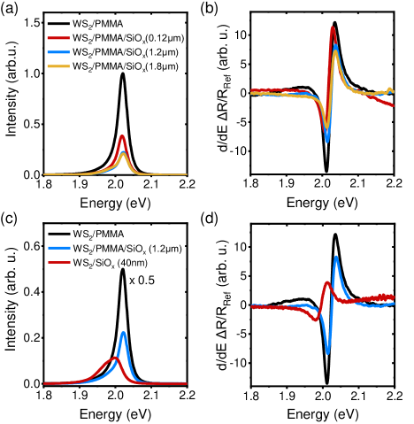
Since the monolayers are fragile and easily damaged by many fabrication techniques including PECVD [20], we further tested how well the PMMA layer protects the monolayer against PECVD of SiOx. The influence of the deposition on the exciton PL and absorption in the PMMA-capped monolayer WS2 is demonstrated in Fig. 3a-b. Clearly, the exciton PL intensity significantly decreases after the deposition process. The observed quenching is stronger with a larger SiOx thickness, which scales with the duration of the deposition. Between the layer thicknesses of 1.2 m SiOx and 1.8 m SiOx the PL intensity remains constant and yields of the PL intensity of the PMMA-capped WS2, which shows that PECVD induced PL quenching saturates at this level. Similarly, the exciton absorption shown in Fig. 3b also decreases after material deposition. This degradation of the PL and oscillator strength could be attributed to the penetration of gaseous plasma (leakage of conductive ions) through the microporous PMMA layer [50]. Once the plasma reaches the monolayer surface, it can degrade the material by creating additional defects, which explains the observed behaviour. Nevertheless, the decrease of excitonic absorption after material deposition is much less compared to that of the excitonic PL. Accordingly, the oscillator strength remains relatively high after deposition of PMMA and SiOx in contrast with the exciton quantum yield.
To further test the protective properties of the PMMA layer, we prepared an uncapped monolayer sample, on which we directly deposited of SiOx via PECVD. This thickness was chosen to maintain some optical response from the exciton in the WS2/SiOx structure [20]. The PL spectra in Fig. 3c reveal that the PL emission of PMMA-capped monolayers with subsequent 1.2 m SiOx deposition is almost twice as strong as that of the uncapped monolayer after deposition of 40 nm SiOx. The reflectance contrast spectra (see Fig. 3d) also show much stronger degradation of the exciton oscillator strength for the uncapped monolayer compared to the capped one. Furthermore, the uncapped monolayer shows a pronounced shoulder in the PL spectrum at likely stemming from trion emission [51, 52, 44], which indicates a significant defect-induced charge doping effect caused by the deposition process [46, 20, 53]. These results clearly highlight that the PMMA layer protects the monolayer against the dielectric deposition by PECVD. Since the thickness of deposited SiOx is directly related to the duration of exposure to plasma, the PMMA-capped monolayer was exposed to the plasma for 30 times longer, but still maintained a larger excitonic response, which confirms the protective function of the PMMA layer.
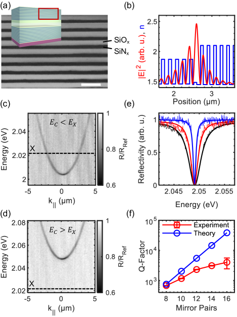
In addition to testing how PMMA and dielectric material deposition affect the optical response of the WS2 excitons at room temperature, we determined the quality of the photon mode that can be achieved in our cavity without the integration of a monolayer. To ensure that the PMMA/SiOx cavity provides a suitable substrate for the top DBR, we perform scanning electron microscope (SEM) imaging on the cross-section of a SiNx/SiOx DBR grown on top of a PMMA layer via PECVD (see Fig. 4a). The SEM image reveals that the SiOx and SiNx layers have a consistent thickness throughout the mirror and a smooth lateral profile on the scale of the light wavelength that is crucial for high optical performance.
Figure 4b presents the simulation of the optical E-field distribution inside an empty cavity with a cavity-length of fulfilling the Bragg condition for , performed with the transfer matrix method [54]. As usual for -cavities [37], the strongly confined resonant E-field has its maximum near the centre of the cavity, which allows for maximum energy exchange between photons and excitons when the monolayer is placed at this position. This is ensured by our sample design, where the last layer of the DBR substrate corresponds to the first half of the cavity spacer. By varying the thickness of the SiOx layer on top of the PMMA layer, both having a similar refractive index, we can fine-tune the cavity length , and therefore, the cavity mode energy EC. This, in turn, enables control of the exciton-photon detuning: = EC-EX, where EX is the exciton energy.
The angle-resolved reflectivity spectra for empty cavities with and of PMMA/SiOx spacer are presented in Fig. 4c-d, respectively, with the top DBRs consisting of 13.5 SiNx/SiOx mirror pairs. The spectra clearly demonstrate the characteristic parabolic dispersion of the cavity photons and show that the photon energy can be tuned well across the exciton energy. The linewidth of the cavity photon can be controlled with the number of mirror pairs of the top DBR (see Fig. 4e), which allows us to increase the quality factor to reaching the resolution limit of our optical setup (see Fig. 4f). These results demonstrate that this sample design enables a good control over both the cavity photon energy and linewidth and allows us to reach much higher Q-factors compared to those of the similarly constructed DBR/metal cavities, e.g., [21, 19, 32] (see Supplementary Table S1). However, to change the exciton-photon detuning, the sample needs to be reproduced with a different thickness of the cavity spacer, and the achievable Q-factors are smaller than the theoretically expected values (see Fig. 4f). The growth of the Q-factor with the number of mirror pairs in the top DBR decreases above 12 pairs, likely due to scattering and absorption processes in the dielectric layers.
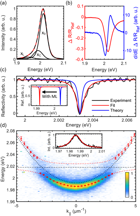
Finally, we fabricated the whole microcavity with an integrated monolayer WS2, as schematically shown in Fig. 1. Figure 5a presents the PL spectrum of a monolayer WS2 placed on the DBR substrate, after deposition of the PMMA spacer (see Fig. 1b). When fitting the spectrum with a three peak Voigt-function accounting for the localised, charged and neutral exciton emission [44] (see Fig. 5a), we can extract the energy and the linewidth of the neutral exciton peak: and , with a contribution of homogeneous broadening and inhomogeneous broadening . The large spectral weight of the neutral exciton is an evidence of the high quality of the DBR substrate causing negligible doping [53] or strain effects [56, 57] in the monolayer, which can reduce exciton-photon interactions and prevent strong light-matter coupling.
The reflectance contrast spectrum and its derivative with respect to the energy (see Fig. 5b) reveal the exciton energy and linewidth , which is in agreement with the Stokes shifted exciton peak of the PL spectrum, and show a significant exciton oscillator strength in the monolayer that ensures a robust exciton-photon interaction strength.
After deposition of the SiOx spacer and the top DBR consisting of 13.5 SiNx/SiOx layer pairs, we characterise the cavity mode away from the monolayer area. Figure 5c shows the measured and theoretical reflectivity spectra of the microcavity with the cavity mode energy and linewidths and , respectively. While the corresponding measured Q-factor is smaller than the theoretical Q-factor , it is similar to the Q-factor of the empty microcavity (see Fig. 4f) and in general, comparable to the largest values reached for microcavities with embedded TMDCs [58, 24, 28, 29, 25] (see Supplementary Table S1).
Figure 5d presents the angle-resolved PL measurement of the whole structure, which was obtained via excitation of the monolayer with a tightly focused laser spot () and collecting the PL in momentum space with a NA=0.65 objective, projected into a 2D spectrometer. The measured dispersion, which decreases in intensity at larger energies due to thermalisation [21, 25], can be approximated with the model of two coupled oscillators [59]:
| (1) |
where are the complex energies of the lossy modes, is the strength of coupling between the cavity photons and the excitons, and (see Fig. 5d). Note, that corresponds to of the measured modes [59].
Using the energies and linewidths of the exciton and cavity resonances (see Fig. 5a-c), we find an excellent agreement between Eq. (1) and the measured dispersion with (see Fig. 5d). The corresponding Hopfield coefficient of the lower polariton branch
| (2) |
allows us to approximate the polariton PL spectrum with a Voigt profile, where , which reproduces the measured PL well (see Fig. 5d, inset). Since and , the sample operates in the strong exciton-photon coupling regime, exhibiting distinct exciton-polariton modes [59]. Hence, the sample fabrication technology presented here is suitable for making high-Q planar microcavities with an integrated atomically-thin WS2 crystal operating in the strong light-matter coupling regime.
In summary, we have developed a scalable approach for making high-quality planar microcavities with integrated atomically-thin semiconductors suitable for hosting exciton-polaritons at room temperature. This is achieved by depositing the two DBRs, a monolayer WS2 and a PMMA/SiOx spacer layer-by-layer. We demonstrate that the PMMA layer has only a minor effect on the WS2 exciton oscillator strength and effectively protects the monolayer against further deposition of the top DBR, which allows for strong light-matter interactions in the structure. Since the PMMA/SiOx spacer and the top DBR cover the whole microchip homogeneously, the functional area of the loaded microcavity is mainly limited by the size of the monolayer, which can be scaled up to cm-scale with recently developed synthesis [60, 61] and exfoliation [62, 63] techniques. Further, the PMMA can be easily patterned by lithography methods, paving the way towards creating polariton lattices, waveguides and other 2D potential landscapes on a microchip, as previously demonstrated for microcavities with embedded perovskites [14, 64].
Acknowledgements
Acknowledgements.
This work was supported by the Australian Research Council (ARC) grants CE170100039 and DE220100712. We acknowledge the Australian National Fabrication Facility (ANFF) OptoFab at its node in the Australian Capital Territory (ACT) for fabricating the DBR substrate and technical support for sample fabrication from the ANFF ACT node.References
- Weisbuch et al. [1992] C. Weisbuch, M. Nishioka, A. Ishikawa, and Y. Arakawa, Observation of the coupled exciton-photon mode splitting in a semiconductor quantum microcavity, Phys. Rev. Lett. 69, 3314 (1992).
- Kasprzak et al. [2006] J. Kasprzak, M. Richard, S. Kundermann, A. Baas, P. Jeambrun, J. M. Keeling, F. M. Marchetti, M. H. Szymánska, R. André, J. L. Staehli, V. Savona, P. B. Littlewood, B. Deveaud, and L. S. Dang, Bose-Einstein condensation of exciton polaritons, Nature 443, 409 (2006).
- Amo et al. [2009] A. Amo, J. Lefrère, S. Pigeon, C. Adrados, C. Ciuti, I. Carusotto, R. Houdré, E. Giacobino, and A. Bramati, Superfluidity of polaritons in semiconductor microcavities, Nature Physics 5, 805 (2009).
- Gao et al. [2015] T. Gao, E. Estrecho, K. Y. Bliokh, T. C. Liew, M. D. Fraser, S. Brodbeck, M. Kamp, C. Schneider, S. Höfling, Y. Yamamoto, F. Nori, Y. S. Kivshar, A. G. Truscott, R. G. Dall, and E. A. Ostrovskaya, Observation of non-Hermitian degeneracies in a chaotic exciton-polariton billiard, Nature 526, 554 (2015).
- Schneider et al. [2013] C. Schneider, A. Rahimi-Iman, N. Y. Kim, J. Fischer, I. G. Savenko, M. Amthor, M. Lermer, A. Wolf, L. Worschech, V. D. Kulakovskii, I. A. Shelykh, M. Kamp, S. Reitzenstein, A. Forchel, Y. Yamamoto, and S. Höfling, An electrically pumped polariton laser, Nature 497, 348 (2013).
- Klembt et al. [2018] S. Klembt, T. H. Harder, O. A. Egorov, K. Winkler, R. Ge, M. A. Bandres, M. Emmerling, L. Worschech, T. C. Liew, M. Segev, C. Schneider, and S. Höfling, Exciton-polariton topological insulator, Nature 562, 552 (2018).
- Christopoulos et al. [2007] S. Christopoulos, G. B. H. von Högersthal, A. J. D. Grundy, P. G. Lagoudakis, A. V. Kavokin, J. J. Baumberg, G. Christmann, R. Butté, E. Feltin, J.-F. Carlin, and N. Grandjean, Room-temperature polariton lasing in semiconductor microcavities, Phys. Rev. Lett. 98, 126405 (2007).
- Guillet et al. [2011] T. Guillet, M. Mexis, J. Levrat, G. Rossbach, C. Brimont, T. Bretagnon, B. Gil, R. Butté, N. Grandjean, L. Orosz, F. Réveret, J. Leymarie, J. Zúñiga-Pérez, M. Leroux, F. Semond, and S. Bouchoule, Polariton lasing in a hybrid bulk ZnO microcavity, Applied Physics Letters 99, 161104 (2011).
- Su et al. [2017] R. Su, C. Diederichs, J. Wang, T. C. H. Liew, J. Zhao, S. Liu, W. Xu, Z. Chen, and Q. Xiong, Room-temperature polariton lasing in all-inorganic perovskite nanoplatelets, Nano Letters 17, 3982 (2017).
- Dietrich et al. [2016] C. P. Dietrich, A. Steude, L. Tropf, M. Schubert, N. M. Kronenberg, K. Ostermann, S. Höfling, and M. C. Gather, An exciton-polariton laser based on biologically produced fluorescent protein, Science Advances 2, 8 (2016).
- Dusel et al. [2021] M. Dusel, S. Betzold, T. H. Harder, M. Emmerling, J. Beierlein, J. Ohmer, U. Fischer, R. Thomale, C. Schneider, S. Höfling, and S. Klembt, Room-temperature topological polariton laser in an organic lattice, Nano Letters 21, 6398 (2021).
- Lerario et al. [2017] G. Lerario, A. Fieramosca, F. Barachati, D. Ballarini, K. S. Daskalakis, L. Dominici, M. D. Giorgi, S. A. Maier, G. Gigli, S. Kéna-Cohen, and D. Sanvitto, Room-temperature superfluidity in a polariton condensate, Nature Physics 13, 837 (2017).
- Su et al. [2021] R. Su, E. Estrecho, D. Biegańska, Y. Huang, M. Wurdack, M. Pieczarka, A. G. Truscott, T. C. H. Liew, E. A. Ostrovskaya, and Q. Xiong, Direct measurement of a non-hermitian topological invariant in a hybrid light-matter system, Science Advances 7, 45 (2021).
- Su et al. [2020] R. Su, S. Ghosh, J. Wang, S. Liu, C. Diederichs, T. C. Liew, and Q. Xiong, Observation of exciton polariton condensation in a perovskite lattice at room temperature, Nature Physics 16, 301 (2020).
- Mak et al. [2010] K. F. Mak, C. Lee, J. Hone, J. Shan, and T. F. Heinz, Atomically thin : A new direct-gap semiconductor, Phys. Rev. Lett. 105, 136805 (2010).
- Liu et al. [2014] X. Liu, T. Galfsky, Z. Sun, F. Xia, E. C. Lin, Y. H. Lee, S. Kéna-Cohen, and V. M. Menon, Strong light-matter coupling in two-dimensional atomic crystals, Nature Photonics 9, 30 (2014).
- Sanvitto and Kéna-Cohen [2016] D. Sanvitto and S. Kéna-Cohen, The road towards polaritonic devices, Nature Materials 15, 1061 (2016).
- Schneider et al. [2018] C. Schneider, M. M. Glazov, T. Korn, S. Höfling, and B. Urbaszek, Two-dimensional semiconductors in the regime of strong light-matter coupling, Nature Communications 9, 2695 (2018).
- Gu et al. [2019] J. Gu, B. Chakraborty, M. Khatoniar, and V. M. Menon, A room-temperature polariton light-emitting diode based on monolayer WS2, Nature Nanotechnology 14, 1024 (2019).
- Yun et al. [2021] T. Yun, M. Wurdack, M. Pieczarka, S. Bhattacharyya, Q. Ou, C. Notthoff, C. K. Nguyen, T. Daeneke, P. Kluth, M. S. Fuhrer, A. G. Truscott, E. Estrecho, and E. A. Ostrovskaya, Influence of direct deposition of dielectric materials on the optical response of monolayer WS2, Applied Physics Letters 119, 133106 (2021).
- Lundt et al. [2016a] N. Lundt, S. Klembt, E. Cherotchenko, S. Betzold, O. Iff, A. V. Nalitov, M. Klaas, C. P. Dietrich, A. V. Kavokin, S. Höfling, and C. Schneider, Room-temperature Tamm-plasmon exciton-polaritons with a WSe2 monolayer, Nature Communications 7, 2695 (2016a).
- Chen et al. [2017] Y. J. Chen, J. D. Cain, T. K. Stanev, V. P. Dravid, and N. P. Stern, Valley-polarized exciton-polaritons in a monolayer semiconductor, Nature Photonics 11, 431 (2017).
- Lundt et al. [2019] N. Lundt, Łukasz Dusanowski, E. Sedov, P. Stepanov, M. M. Glazov, S. Klembt, M. Klaas, J. Beierlein, Y. Qin, S. Tongay, M. Richard, A. V. Kavokin, S. Höfling, and C. Schneider, Optical valley Hall effect for highly valley-coherent exciton-polaritons in an atomically thin semiconductor, Nature Nanotechnology 14, 770 (2019).
- Rupprecht et al. [2021] C. Rupprecht, N. Lundt, M. Wurdack, P. Stepanov, E. Estrecho, M. Richard, E. A. Ostrovskaya, S. Höfling, and C. Schneider, Micro-mechanical assembly and characterization of high-quality Fabry–Pérot microcavities for the integration of two-dimensional materials, Applied Physics Letters 118, 103103 (2021).
- Wurdack et al. [2021] M. Wurdack, E. Estrecho, S. Todd, T. Yun, M. Pieczarka, S. K. Earl, J. A. Davis, C. Schneider, A. G. Truscott, and E. A. Ostrovskaya, Motional narrowing, ballistic transport, and trapping of room-temperature exciton polaritons in an atomically-thin semiconductor, Nature Communications 12, 5366 (2021).
- Anton-Solanas et al. [2021] C. Anton-Solanas, M. Waldherr, M. Klaas, H. Suchomel, T. H. Harder, H. Cai, E. Sedov, S. Klembt, A. V. Kavokin, S. Tongay, K. Watanabe, T. Taniguchi, S. Höfling, and C. Schneider, Bosonic condensation of exciton–polaritons in an atomically thin crystal, Nature Materials 20, 1233 (2021).
- Zhao et al. [2022] J. Zhao, A. Fieramosca, R. Bao, W. Du, K. Dini, R. Su, J. Feng, Y. Luo, D. Sanvitto, T. C. Liew, and Q. Xiong, Nonlinear polariton parametric emission in an atomically thin semiconductor based microcavity, Nature Nanotechnology 17, 396 (2022).
- Knopf et al. [2019] H. Knopf, N. Lundt, T. Bucher, S. Höfling, S. Tongay, T. Taniguchi, K. Watanabe, I. Staude, U. Schulz, C. Schneider, and F. Eilenberger, Integration of atomically thin layers of transition metal dichalcogenides into high-Q, monolithic Bragg-cavities: an experimental platform for the enhancement of the optical interaction in 2D-materials, Optical Materials Express 9, 598 (2019).
- Shan et al. [2021] H. Shan, L. Lackner, B. Han, E. Sedov, C. Rupprecht, H. Knopf, F. Eilenberger, J. Beierlein, N. Kunte, M. Esmann, K. Yumigeta, K. Watanabe, T. Taniguchi, S. Klembt, S. Höfling, A. V. Kavokin, S. Tongay, C. Schneider, and C. Antón-Solanas, Spatial coherence of room-temperature monolayer WSe2 exciton-polaritons in a trap, Nature Communications 12, 6406 (2021).
- Waldherr et al. [2018] M. Waldherr, N. Lundt, M. Klaas, S. Betzold, M. Wurdack, V. Baumann, E. Estrecho, A. Nalitov, E. Cherotchenko, H. Cai, E. A. Ostrovskaya, A. V. Kavokin, S. Tongay, S. Klembt, S. Höfling, and C. Schneider, Observation of bosonic condensation in a hybrid monolayer MoSe2-GaAs microcavity, Nature Communications 9, 3286 (2018).
- Lundt et al. [2017] N. Lundt, P. Nagler, A. Nalitov, S. Klembt, M. Wurdack, S. Stoll, T. H. Harder, S. Betzold, V. Baumann, A. V. Kavokin, C. Schüller, T. Korn, S. Höfling, and C. Schneider, Valley polarized relaxation and upconversion luminescence from Tamm-plasmon trion-polaritons with a MoSe2 monolayer, 2D Materials 4, 025096 (2017).
- Wurdack et al. [2017] M. Wurdack, N. Lundt, M. Klaas, V. Baumann, A. V. Kavokin, S. Höfling, and C. Schneider, Observation of hybrid Tamm-plasmon exciton-polaritons with GaAs quantum wells and a MoSe2 monolayer, Nature Communications 8, 259 (2017).
- Gu et al. [2021] J. Gu, V. Walther, L. Waldecker, D. Rhodes, A. Raja, J. C. Hone, T. F. Heinz, S. Kéna-Cohen, T. Pohl, and V. M. Menon, Enhanced nonlinear interaction of polaritons via excitonic rydberg states in monolayer WSe2, Nature Communications 12, 2269 (2021).
- Datta et al. [2021] B. Datta, M. Khatoniar, P. Deshmukh, R. Bushati, S. De Liberato, S. K. Cohen, and V. M. Menon, Highly non-linear interlayer exciton-polaritons in bilayer MoS2, arXiv:2110.13326 (2021).
- Zhao et al. [2021] J. Zhao, R. Su, A. Fieramosca, W. Zhao, W. Du, X. Liu, C. Diederichs, D. Sanvitto, T. C. H. Liew, and Q. Xiong, Ultralow threshold polariton condensate in a monolayer semiconductor microcavity at room temperature, Nano Letters 21, 3331 (2021).
- [36] The fabrication of the high-reflectivity substrate was peformed at the ACT OptoFab node of the Australian National Fabrication Facility - a company established under the National Collaborative Research Infrastructure Strategy to provide nano and microfabrication facilities for Australia’s researchers .
- Kavokin et al. [2017] A. Kavokin, J. Baumberg, G. Malpuech, and F. Laussy, Microcavities, Series on Semiconductor Science and Technology (OUP Oxford, 2017).
- [38] http://www.hqgraphene.com.
- [39] http://www.novawafers.com.
- Zeng et al. [2013] H. Zeng, G. B. Liu, J. Dai, Y. Yan, B. Zhu, R. He, L. Xie, S. Xu, X. Chen, W. Yao, and X. Cui, Optical signature of symmetry variations and spin-valley coupling in atomically thin tungsten dichalcogenides, Scientific Reports 3, 1608 (2013).
- Mueller and Malic [2018] T. Mueller and E. Malic, Exciton physics and device application of two-dimensional transition metal dichalcogenide semiconductors, npj 2D Materials and Applications 2, 29 (2018).
- Lundt et al. [2016b] N. Lundt, A. Maryński, E. Cherotchenko, A. Pant, X. Fan, S. Tongay, G. Sek, A. V. Kavokin, S. Höfling, and C. Schneider, Monolayered MoSe2: a candidate for room temperature polaritonics, 2D Materials 4, 015006 (2016b).
- Tongay et al. [2013a] S. Tongay, J. Suh, C. Ataca, W. Fan, A. Luce, J. S. Kang, J. Liu, C. Ko, R. Raghunathanan, J. Zhou, F. Ogletree, J. Li, J. C. Grossman, and J. Wu, Defects activated photoluminescence in two-dimensional semiconductors: Interplay between bound, charged, and free excitons, Scientific Reports 3, 2657 (2013a).
- Shang et al. [2015] J. Shang, X. Shen, C. Cong, N. Peimyoo, B. Cao, M. Eginligil, and T. Yu, Observation of excitonic fine structure in a 2D transition-metal dichalcogenide semiconductor, ACS Nano 9, 647 (2015).
- Carozo et al. [2017] V. Carozo, Y. Wang, K. Fujisawa, B. R. Carvalho, A. McCreary, S. Feng, Z. Lin, C. Zhou, N. Perea-López, A. L. Elías, B. Kabius, V. H. Crespi, and M. Terrones, Optical identification of sulfur vacancies: Bound excitons at the edges of monolayer tungsten disulfide, Science Advances 3, 4 (2017).
- Sebait et al. [2021] R. Sebait, C. Biswas, B. Song, C. Seo, and Y. H. Lee, Identifying defect-induced trion in monolayer WS2 via carrier screening engineering, ACS Nano 15, 2849 (2021).
- Tongay et al. [2013b] S. Tongay, J. Zhou, C. Ataca, J. Liu, J. S. Kang, T. S. Matthews, L. You, J. Li, J. C. Grossman, and J. Wu, Broad-range modulation of light emission in two-dimensional semiconductors by molecular physisorption gating, Nano Letters 13, 2831 (2013b).
- Zhang et al. [2019] F. Zhang, Y. Lu, D. S. Schulman, T. Zhang, K. Fujisawa, Z. Lin, Y. Lei, A. L. Elias, S. Das, S. B. Sinnott, and M. Terrones, Carbon doping of WS2 monolayers: Bandgap reduction and p-type doping transport, Science Advances 5, 5 (2019).
- Gao et al. [2016] J. Gao, B. Li, J. Tan, P. Chow, T.-M. Lu, and N. Koratkar, Aging of transition metal dichalcogenide monolayers, ACS Nano 10, 2628 (2016).
- Charlot et al. [2011] B. Charlot, S. Gauthier, A. Garraud, P. Combette, and A. Giani, Pvdf/pmma blend pyroelectric thin films, Journal of Materials Science: Materials in Electronics 22, 1766 (2011).
- Mak et al. [2013] K. F. Mak, K. He, C. Lee, G. H. Lee, J. Hone, T. F. Heinz, and J. Shan, Tightly bound trions in monolayer MoS2, Nature Materials 12, 207 (2013).
- Zhu et al. [2015] B. Zhu, X. Chen, and X. Cui, Exciton binding energy of monolayer WS2, Scientific Reports 5, 9218 (2015).
- Martín-Sánchez et al. [2018] J. Martín-Sánchez, A. Mariscal, M. D. Luca, A. T. Martín-Luengo, G. Gramse, A. Halilovic, R. Serna, A. Bonanni, I. Zardo, R. Trotta, and A. Rastelli, Effects of dielectric stoichiometry on the photoluminescence properties of encapsulated WSe2 monolayers, Nano Research 11, 1399 (2018).
- Born et al. [2000] M. Born, E. Wolf, and A. Bhatia, Principles of Optics: Electromagnetic Theory of Propagation, Interference and Diffraction of Light (Cambridge University Press, 2000).
- Li et al. [2014] Y. Li, A. Chernikov, X. Zhang, A. Rigosi, H. M. Hill, A. M. van der Zande, D. A. Chenet, E.-M. Shih, J. Hone, and T. F. Heinz, Measurement of the optical dielectric function of monolayer transition-metal dichalcogenides: , , , and , Phys. Rev. B 90, 205422 (2014).
- Khatibi et al. [2018] Z. Khatibi, M. Feierabend, M. Selig, S. Brem, C. Linderälv, P. Erhart, and E. Malic, Impact of strain on the excitonic linewidth in transition metal dichalcogenides, 2D Materials 6, 015015 (2018).
- He et al. [2013] K. He, C. Poole, K. F. Mak, and J. Shan, Experimental demonstration of continuous electronic structure tuning via strain in atomically thin MoS2, Nano Letters 13, 2931 (2013).
- Sidler et al. [2017] M. Sidler, P. Back, O. Cotlet, A. Srivastava, T. Fink, M. Kroner, E. Demler, and A. Imamoglu, Fermi polaron-polaritons in charge-tunable atomically thin semiconductors, Nature Physics 13, 255 (2017).
- Savona et al. [1995] V. Savona, L. Andreani, P. Schwendimann, and A. Quattropani, Quantum well excitons in semiconductor microcavities: Unified treatment of weak and strong coupling regimes, Solid State Communications 93, 733 (1995).
- Lee et al. [2017] J. Lee, S. Pak, P. Giraud, Y.-W. Lee, Y. Cho, J. Hong, A.-R. Jang, H.-S. Chung, W.-K. Hong, H. Y. Jeong, H. S. Shin, L. G. Occhipinti, S. M. Morris, S. Cha, J. I. Sohn, and J. M. Kim, Thermodynamically stable synthesis of large-scale and highly crystalline transition metal dichalcogenide monolayers and their unipolar n–n heterojunction devices, Advanced Materials 29, 1702206 (2017).
- Choi et al. [2022] S. H. Choi, S. J. Yun, Y. S. Won, C. S. Oh, S. M. Kim, K. K. Kim, and Y. H. Lee, Large-scale synthesis of graphene and other 2D materials towards industrialization, Nature Communications 13, 1484 (2022).
- Desai et al. [2016] S. B. Desai, S. R. Madhvapathy, M. Amani, D. Kiriya, M. Hettick, M. Tosun, Y. Zhou, M. Dubey, J. W. Ager III, D. Chrzan, and A. Javey, Gold-mediated exfoliation of ultralarge optoelectronically-perfect monolayers, Advanced Materials 28, 4053 (2016).
- Liu et al. [2020] F. Liu, W. Wu, Y. Bai, S. H. Chae, Q. Li, J. Wang, J. Hone, and X.-Y. Zhu, Disassembling 2d van der waals crystals into macroscopic monolayers and reassembling into artificial lattices, Science 367, 903 (2020).
- Su et al. [2018] R. Su, J. Wang, J. Zhao, J. Xing, W. Zhao, C. Diederichs, T. C. H. Liew, and Q. Xiong, Room temperature long-range coherent exciton polariton condensate flow in lead halide perovskites, Science Advances 4, 10 (2018).