Optical response of two-dimensional Dirac materials with a flat band
Abstract
Two-dimensional Dirac materials with a flat band have been demonstrated to possess a plethora of unusual electronic properties, but the optical properties of these materials are less studied. Utilizing - lattice as a prototypical system, where is a tunable parameter and a flat band through the conic intersection of two Dirac cones arises for , we investigate the conductivity of flat-band Dirac material systems analytically and numerically. Motivated by the fact that the imaginary part of the optical conductivity can have significant effects on the optical response and is an important factor of consideration for developing - lattice based optical devices, we are led to derive a complete conductivity formula with both the real and imaginary parts. Scrutinizing the formula, we uncover two phenomena. First, for the value of in some range, two types of optical transitions coexist: one between the two Dirac cones and another from the flat band to a cone, which generate multi-frequency transverse electrical propagating waves. Second, for so the quasiparticles become pseudospin-1, the flat-to-cone transition can result in resonant scattering. These results pave the way to exploiting - lattice for optical device applications in the terahertz frequency domain.
I Introduction
Quantum materials whose energy band consists of a pair of Dirac cones and a topologically flat band, electronic or optical, constitute a frontier area of research [1, 2, 3, 4, 5, 6, 7, 8, 9, 10, 11, 12, 13, 14, 15, 16, 17, 18, 19, 20, 21, 22, 23, 24, 25, 26, 27, 28]. For example, in a dielectric photonic crystal, Dirac cones can be induced by accidental degeneracy occurring at the center of the Brillouin zone, which effectively makes the crystal a zero-refractive-index metamaterial at the Dirac point where the Dirac cones intersect with another flat band [7, 8, 9, 14, 18]. Alternatively, configuring an array of evanescently coupled optical waveguides into a Lieb lattice [11, 15, 16, 19] can lead to a gapless spectrum consisting of a pair of common Dirac cones and a perfect flat middle band at the corner of the Brillouin zone. Loading cold atoms into an optical Lieb lattice provides another experimental realization of the gapless three-band spectrum at a smaller scale with greater dynamical controllability of the system parameters [17]. Dice or optical lattices also possess the Dirac cone and flat-band structure [29, 30, 2, 5, 10, 31]. Electronically, Dirac materials that can generate a topologically flat band include transition-metal oxide SrTiO3/SrIrO3/SrTiO3 trilayer heterostructures [6], D carbon or MoS2 allotropes with a square symmetry [32], as well as SrCu2(BO3)2 [12] and graphene-In2Te2 bilayer [13].
In two-dimensional (2D) Dirac materials with a flat band, the quasiparticles are of the massless or massive pseudospin-1 type. Comparing with the conventional Dirac cone systems with massless pseudospin-1/2 quasiparticles (e.g., graphene) [33, 34], pseudospin- systems can exhibit quite unusual and unconventional physics such as super-Klein tunneling for the two conical, linearly dispersive bands [3, 35, 5, 18, 36], diffraction-free wave propagation and novel conical diffraction [11, 15, 16, 19], flat-band rendered divergent DC conductivity with a tunable short-range disorder [37], unconventional Anderson localization [38, 39], flat-band ferromagnetism [40, 41, 17], and peculiar topological phases under external gauge fields or spin-orbit coupling [42, 43, 6, 44]. In particular, topological phases arise due to the flat band that permits a number of degenerate localized states with a topological origin, i.e., “caging” of carriers [45]. Additional phenomena include superscattering of pseudospin-1 waves in the subwavelength regime [46], geometric valley Hall effect and and valley filtering [47], chaos based Berry phase detection [48], atomic collapse in pseudospin-1 systems [49], anomalous chiral edge states in spin-1 Dirac-Weyl quantum dots [50], anomalous in-gap edge states in two-dimensional pseudospin-1 Dirac-Weyl insulators [51], and the analogy between Klein scattering of spin-1 Dirac-Weyl wave and localized surface plasmon [52]. There was also a study of interplay between classical chaos and flat-band physics [53]. In the past few years, magic-angle twisted bilayer graphene, a type of quantum materials hosting a flat band, has become a forefront area of research. These materials can generate surprising physical phenomena such as superconductivity [54, 55], orbital ferromagnetism [56, 57], and the Chern insulating behavior with topological edge states. Notwithstanding the diversity and the broad scales to realize the band structure that consists of two conical bands and a characteristic flat band intersecting at a single point in different physical systems, theoretically a unified framework exists: the generalized Dirac-Weyl equation for massless or massive spin-1 particles [2, 36].
The optical properties of 2D Dirac materials without a flat band have been extensively investigated, such as the optical responses of graphene [58, 59, 60, 61], its theoretically predicted frequency-dependent optical conductivity [62, 63, 64, 65, 66, 67] and experimental verification [68, 69, 70], suggesting the possibility of developing graphene-based tunable terahertz optical devices. Such devices can have applications ranging from light transform [58, 71, 72] and high frequency communication [73, 74, 75] to cloaking or superscattering [76, 77]. In particular, the discovery of novel plasmon mode in graphene led to the first experimental superscattering system at a macroscopic scale [78]. These efforts have given birth to new fields such as topological photonics [79, 80] and topological lasing [81, 82]. Besides single-layer graphene, the optical properties of other 2D material have also been studied. For example, surface plasmon has been uncovered and characterized in hexagonal boron nitride (hBN) or graphene hBN hybrid structures [83, 84], in bilayer [65, 85] and multilayer [86, 87] graphene, in twisted graphene bilayer [88, 89, 90, 91, 92], in silicene [93] and hyperbolic materials [94, 95]. Particularly worth mentioning is the work on the conductivity for gapped Dirac fermions [96], where the Kubo formula was used to calculate the contribution of the intra-band transitions to the optical conductivity. A central goal in these studies is to garner a strong optical response at certain frequency or at multiple frequencies. In 2D Dirac materials without a flat band, transverse magnetic (TM, or -polarized) and transverse electric (TE, or -polarized) polaritons have been found to emerge at different frequencies, where the TE polarization can arise at high frequencies with a low loss [66].
For Dirac materials with a flat band, most previous work focused on their electronic properties: their optical properties have been less studied. In this paper, we investigate the “complete” optical responses of 2D Dirac materials with a flat band, in the sense that both the real and imaginary parts of the optical conductivity are derived, using the - lattice as a paradigmatic model system of such materials. This lattice is formed by adding an atom at the center of each unit cell of the honeycomb graphene lattice [2], where the low energy excitations can be described by the pseudospin-1 Dirac-Weyl equation. The parameter characterizes the interaction strength between the central atom and any of its nearest neighbors, relative to that between two neighboring atoms at the vertices of the hexagonal cell. For there is no coupling between the central atom and a vertex , so the lattice degenerates to graphene with pseudospin-1/2 quasiparticles. As the value of increases from zero to one, a flat band through the conic interaction of the two Dirac cones emerges and its physical influences become progressively pronounced [10, 97]. For , the lattice generates pseudospin-1 quasiparticles. The flat band can lead to physical phenomena such as the divergence of conductivity [37, 98, 49]. Under a continuous approximation, an - lattice can be treated as a thin layer with certain surface conductivity. Unlike graphene, here the surface conductivity is contributed to by three types of transitions between the bands: intraband transition, cone-to-cone transition, and flat-band-to-cone transition. Previously, the optical conductivity of - lattice was “partially” studied in the sense that only the real part of the conductivity has been derived [97, 99, 100, 101]. Considering that the imaginary part can affect the optical response significantly and is therefore important for developing - lattice based optical devices, we are led to derive a complete conductivity formula with both the real and imaginary parts. The formula is verified through two independent approaches and leads to two previously uncovered phenomena. First, while the intraband transition leads to TM polarized waves at low frequencies (1-10 THz), TE polarized waves can emerge at high frequencies (100-300 THz), due to the two interband transitions. Second, the unique flat-band-to-cone transition generates multi-frequency TE propagating waves for and a strong optical response for . These phenomena are confirmed through studying the behaviors of propagating surface wave and scattering.
We remark that a viable experimental way to realize - lattice is through photonic crystals [29, 27, 102, 103], where the three nonequivalent atoms in a unit cell can be simulated by using coupled waveguides generated by laser inscription [103]. Electronic materials can also be exploited to generate pseudospin-1 lattice systems such as transition-metal oxide trilayer heterostructures [6], [12] or graphene- [13]. Recently, materials with a flat band have been reported [104] A review of the experimentally realized dice-like system can be found in Ref. [105]. The physics of certain solid-state materials is effectively that of an - lattice. For example, a theoretical analysis and computations showed [106] that the material is equivalent to the - lattice with . This material has been realized in experiments [107, 108, 109]. For this reason, we emphasize the case of in this paper.
In Sec. II, we describe the optical conductivity for - lattice, which consists of three parts, and we use two different methods to derive the conductivity. In Sec. III, we solve the Maxwell’s equations for - lattice in a dielectric medium and characterize the properties of the TM and TE polarized waves using the loss and attenuation length. In Sec. IV, we study optical scattering from a sphere coated with - lattice and discuss potential optical device applications. Conclusions and a discussion are offered in Sec. V.
II Optical conductivity of - lattice
An - lattice is generated by placing an additional atom at the center of each unit cell of the honeycomb lattice, where there are three nonequivalent atoms, as shown in Fig. 1(a). The range of the variation of the parameter is , where the quasiparticles are pseudospin-1/2 for and pseudospin-1 for , and a flat band arises for . For convenience, we say that the quasiparticles for are of the “hybrid” type. Under the tight-binding approximation, the low-energy excitation Hamiltonian is given by [10, 97]
| (1) |
where , , is the Fermi velocity, and denotes the valley index. Solving the eigenvalue problem associated with the tight-binding Hamiltonian matrix, we obtain three eigenfunctions, as detailed in Appendix A. There are three distinct energy bands: a pair of Dirac cones and a flat band, as shown in Fig. 1(b).
The optical properties of the - lattice are largely controlled by the surface conductivity , which is determined by the expectation value of the current operator. In the direction as specified in Fig. 1(c), the current operator is , where
| (2) |
Expanding the current vector in the three bands, we obtain the matrix representation of , as described in Appendix A. For weak electrical field, the conductivity is given by the standard Kubo formula [63, 67]
| (3) |
where the subscript in indicates the direction of the current and electric field, and is the frequency of the electromagnetic wave. For a homogeneous material without a magnetic field, we have and . The summation is over all states and with the respective energy and . Evaluating the integral, the nonzero terms appear only for [110] . The quantity in Eq. (3) stands for the Fermi-Dirac distribution. At zero temperature, the only transitions allowed are those from the filled to the unfilled bands, or vice versa.
To obtain the optical conductivity, it is necessary to evaluate the summation in the Kubo formula Eq. (3). The details of the derivation are presented in Appendix B.1. The validity of the derivation and the result can be established by using the Kramers–Kronig (KK) relation as described in Appendix B.2, which gives the same results. Here we summarize our complete conductivity formulas.
Physically, momentum conservation stipulates that the summation for and can be regarded as corresponding to band transition processes. In particular, the summation can be divided into three parts, denoted as , and , which correspond to the intraband, cone-to-cone and flat-band-to-cone transitions, respectively. The conductivity due to the intraband transition is
| (4) |
where and is the chemical potential. The Drude peak is represented by a -function with the coefficient proportional to the chemical potential . The conductivity due to the cone-to-cone transition is
| (5) |
where is the Heaviside step function. The conductivity due to the flat-band-to-cone transition is
| (6) |
For convenience, we introduce a unit free conductivity and divide it into real and imaginary parts
| (7) |
At finite temperatures, the Fermi-Dirac distribution is no longer a step function and this will lead to a change in the conductivity formula, as detailed in Appendix B.3.
We have also analyzed the effect of finite impurity scattering on the optical conductivity, as detailed in Appendix B.4. The main result is that finite impurity scattering will change the conductivity as in Eq. (4) for .
For 2D Dirac materials such as graphene, the high frequency regime above THz is physically important for the optical conductivity. Nonetheless, the behavior of the conductivity in the low frequency regime can be analyzed in terms of the product between the frequency and the imaginary part of the conductivity (see Appendix B.5). This is motivated by the fact that, in the study of optical conductivity of superconducting materials, the quantity is often used to characterize the penetration depth [111, 112, 113]. We also study the effects of varying on the optical conductivity and find that the flat band does not play a significant role in the conductivity in the low frequency regime. However, decreasing the Fermi energy or increasing the temperature can make the flat-band contribution more pronounced. The different relaxation time for different values of can also impact the optical conductivity.
For (or equivalently, ), our conductivity formula reduces to the one for graphene [62, 63, 64, 65, 66, 67], which was experimentally verified [68, 69, 70]. For , the real part of the conductivity is consistent with the previous result [97]. The imaginary part of the conductivity is the contribution of our present work.
Features of the derived conductivity formulas Eqs. (4-6), are as follows. First, the conductivity does not depend on the detailed lattice structure, insofar as there are a pair of Dirac cones and a flat band. In fact, the conductivity is determined by the linear dispersion relationship and the flat band. Our derivation thus holds for different types of lattices described by the effective Hamiltonian in (1). Second, the formulas hold only for a reasonable range in or . If the value of is small, impurity scattering will be important and, in this case, it is necessary to make the change , where is the relaxation time. This change will smooth out the -function in the intraband conductivity formula.
For the - model, the value of the relaxation time has not been available yet, but insights can be gained by considering graphene, where the experimentally measured [114] relaxation time is about s. Since the optical response of graphene is appreciable at high frequencies above THz, a relaxation time on the order of s means that the direction of the field changes much faster than that in the scattering caused by impurity. In this case, impurity scattering can be ignored [115]. If the value of approaches zero, the conductivity in Eq. (4) will diverge, which is related to the minimal conductivity problem in graphene that remains unresolved [116]. If the value of or is too large, another difficulty arises for the effectively Hamiltonian. For graphene in the regime of visible light, it was shown [117] that the next nearest neighbor hopping leads to only small corrections to the Dirac cone, due to the fact that the nearest hopping energy in graphene is high ( eV), which corresponds to a photon of frequency of several hundred Terahertz. For the pseudospin-1 Lieb lattice, experiments showed that the nearest neighbor hopping energy is smaller than that in graphene [27], but for the dice lattice there has been no experimental result.
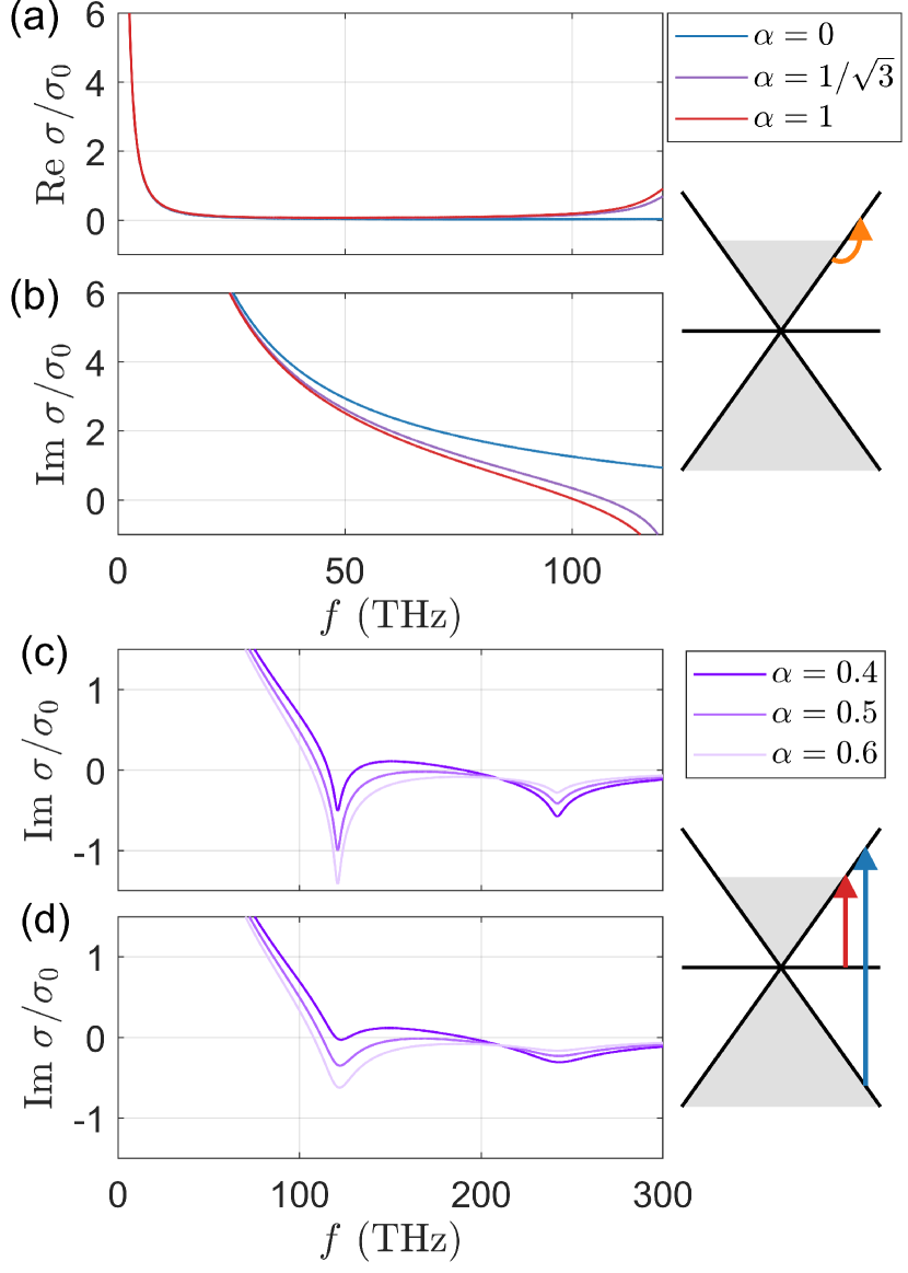
Figure 2 shows the optical conductivity for different values of at a finite temperature. The real part of the conductivity is exemplified in Figs. 2(a), 2(c), and 2(e), to which the intraband process has no contribution. There are two interband transition points, one is the cone-to-cone transition that occurs for and another is the flat-band-to-cone transition that occurs for . (Note that, for , there is no flat band, so the latter transition does not exist.) For , only the flat-band-to-cone transition exists and its magnitude is twice of that of the cone-to-cone transition for . For the hybrid lattice, both types of transitions coexist. A finite temperature tends to smooth the transitions. Figures 2(b), 2(d), and 2(f) show the imaginary part of the conductivity, where the intraband process gives a singularity at , and each interband transition leads to a dip for Im , which is smoothed at finite temperatures. A previous study for graphene demonstrated that, when the imaginary part of the conductivity becomes negative, a new TE mode can emerge [66]. Physically, it would be interesting to investigate the significance of a negative imaginary part of the optical conductivity for the - lattice.
III Intrinsic plasmon modes in - lattice
An important manifestation of the electromagnetic response of 2D Dirac materials is the intrinsic plasmon modes. Specifically, for 2D materials on a dielectric substrate, the Maxwell’s equations can be solved analytically, where the propagating modes follow certain dispersion relationship which depends on the polarization. A solution method was developed earlier [118, 119] and later adopted to graphene [66, 67]. The propagating modes determine the electromagnetic response of the 2D material and they are also termed “intrinsic plasmon modes” [59]. Recently, the study of the plasmon modes has been extended to other kinds of materials such as bilayer graphene [85], twisted bilayer graphene [88], silicene [93], and hBN [84].
Here we study the intrinsic plasmon modes for - lattice. Suppose we embed the lattice in-between two materials with dielectric constants and , respectively, as illustrated in Fig. 1(c). The wavevector is in the -plane and decays along the direction. Neglecting the thickness of the lattice and matching the boundary conditions at , we obtain the polarization-dependent (e.g., TM or TE) dispersion relation [67, 93]. In particular, for the TM polarization, we have
| (8) |
where is the frequency of the incident field and is the speed of light. The solution exists for Im . For 2D materials, the conductivity for small incident frequency is described by the Drude model [118, 119]. For TE polarization, the dispersion relation is
| (9) |
where the solution exists for Im . As revealed by previous work on graphene [66], novel TE polarization can arise for . This can be seen from Fig. 2(b), where the interband transition leads to non-zero negative imaginary conductivity.
TE polarization is a unique feature originated from the linear dispersion relationship, which arises for relatively high frequencies. Previous work revealed that the TE transition can be exploited to develop graphene-based polarizer in the visible light regime [71] and high-frequency optical switches [72]. The negative imaginary conductivity leading to TE polarization was exploited to construct a superscattering system with a curved copper-coated cylinder [78], where a large scattering cross section was obtained even when the dimension of the scatterer is much smaller than the wavelength.
The solution of Eqs. (8) and (9) exist for nonzero imaginary conductivity, but not all the solutions correspond to propagating modes. To characterize wave propagation in the lattice, we use the loss and attenuation length. In particular, the loss is defined as
| (10) |
which determines the average propagation length in the 2D lattice (a small loss leads to longer propagation). The attenuation length or skin depth is defined as [67]
| (11) |
where is a wave vector measuring the confinement in the direction perpendicular to the lattice plane. The strength of the wave in the direction is proportional to and
A small value of corresponds to strong decay in the direction so the wave is well localized in the lattice plane. It is often desired to have a small loss and strong confinement at the same time, but there is a trade-off. In general, TM waves tend to have strong confinement with a large loss, but TE waves have a small loss with weak confinement [67].
We calculate the loss and confinement properties for electromagnetic wave propagation in the - lattice and compare with those of graphene. We consider a finite temperature (e.g., or ) and make the conductivity dimensionless through , where is decomposed into a real and an imaginary parts: . For the TM wave, inserting the conductivity formula into Eq. (8), we get
| (12) |
where is the fine structure constant. The small denominator in the second term leads to a large imaginary value of , so the loss is large for TM waves. For TE waves, we have
| (13) |
where is dimensionless and is small so the Taylor expansion has been used for the square root. Since the loss is proportional to , it is small for TE waves.
The attenuation lengths for the TM and TE waves are
| (14) |
We first study TM wave propagation in - lattice for different values. Since TM polarization occurs only for , the underlying waves arise for small values for which the intraband transition dominates. Figures 3(a), 3(c) and 3(e) show the loss versus the incident frequency for three different values, respectively, from Eqs. (10) and (12). The loss is small when there is strong intraband transition (). The loss becomes large when interband transition is about to happen. As the temperature increases, the loss become larger but this effect is insignificant. Figures 3(b), 3(d) and 3(f) display the attenuation length for TM waves. From Eq. (14), we have that, if the conductivity is purely imaginary, the attenuation length is proportional to . As a result, for the attenuation length is large. As the temperature increases, the sharp dips in the attenuation length are smoothed out. As the value of increases, the flat-band-to-cone transition begins to dominate, making the imaginary part of the conductivity negative for small , so the viable region for TM wave propagation becomes smaller.
Next we study TE wave propagation in the - lattice according to Eqs. (10) and (13). Figures 4(a), 4(c) and 4(e) show the loss versus the incident frequency for three different values of , respectively, and the corresponding results for the attenuation length are shown in Figs. 4(b), 4(d) and 4(f). The loss is smaller than due to the small imaginary part. After interband transition arises, the loss increases due to the finite positive real value of the conductivity. From Eq. (14), we see that the attenuation length is inversely proportional to , so at the transition point the wave is maximally localized. Note that, as , even when the loss decreases, the attenuation length increases, inhibiting the propagating wave. In each panel of Fig. 4, the shaded regions represent those with relatively low loss and small attenuation length. For example, for , this occurs before the cone-to-cone transition, i.e., for , which agrees with the previous result for graphene [66]. For , there are two shaded regions due to the coexistence of two transitions. For , there is one shaded region due to the flat-band-to-cone transition. A higher temperature can lead to an increase in both the loss and attenuation length.
To summarize these results briefly, we have that, for TM waves, the loss is high - typically about to but the attenuation length is small, so the TM waves are highly localized with high loss. Because of the positive imaginary part of the conductivity , as increases the propagation region shrinks. For TE waves, the loss is low - typically less than but the attenuation length is large, so the waves are weakly localized. As increases from zero, the bandwidth for propagation first increases due to the coexistence of multi-interband processes. For , the flat-band-to-cone transition has a large magnitude and is the only process present.
There are two unique features of electromagnetic wave propagation in the - lattice. First, comparing panels (a,b) with (e,f) in Fig. 4, we have that the TE waves for pseudospin-1 lattice have a narrow frequency width and a small attenuation length, indicating that the intrinsic plasmon mode is strongly localized, which is due to the transition from the flat-band to the linear band. Second, Figs. 4(c) and 4(d) indicate that multiple frequency TE polarization waves can arise: one is the same as graphene at due to the cone-to-cone transition and another occurs at , which is due to the flat-band-to-cone transition. For eV, the linear dispersion relation holds, so the regions that can support TE wave propagation correspond to 110–125 THz and 190–240 THz at the room temperature ( - about K).
We have studied the effect of impurity scattering on the optical conductivity. Figures 5(a) and 5(b) display the conductivity curve in the frequency range THz in the presence of finite impurity scattering. The value of the relaxation time is taken to be that of graphene () [115], as the experimental value of this time for has not been available yet. It can be seen that finite impurity scattering can change the real part of the intraband conductivity and smooth out the -function. However, the change mainly occurs for frequencies below 10THz and is generally insignificant. In fact, for frequencies above 100THz, finite impurity scattering has little effect on the optical conductivity. Our formula of the intraband conductivity also suggests that it depends on the relaxation time but not on the value of . We note that a similar observation was made earlier [97].
The interval in in which the two TE polarization waves arise can be seen from Figs. 5(c) and 5(d). At low temperatures, there are two distinct local minima generated by interband transitions for . When the temperature increases to , the interval shrinks. This phenomenon can be understood, as follows. According to Eqs. (5) and (6), the strength of the cone-to-cone transition is proportional to and that of the flat-band-to-cone transition is proportional to , where . Without taking into consideration intraband transitions, the two types of interband transition would have the same magnitude for , which correspond to . From Eq. (4), intraband transitions give a positive imaginary value in the conductivity and the interband transitions generate a negative imaginary value. Since the strength of intraband transitions is inversely proportional to , the effective strength of the flat-band-to-cone transition is reduced. To have approximately the same strength for the cone-to-cone and flat-band-to-cone transitions, it is necessary to increase the value of to facilitate the flat-band-to-cone transition. Numerically, the optimal interval in which the two types of interband transition are approximately equal can be obtained by monitoring the respective local minima in the conductivity generated by the transitions and examining when the two local minima reach a similar magnitude. From Response Figs. 5(c) and 5(d), we note that the two local minima are similar for . At finite temperatures, the local minima will be smoothed out, so the interval shrinks as the temperature increases.
IV Resonant scattering from an - lattice coated dielectric sphere
In electromagnetics, for applications such as optical sensing, imaging, tagging and spectroscopy [120, 121, 122], enhanced scattering is desired. There are also applications where reduced scattering is sought, such as cloaking [123, 124], which can be realized through the technique of scattering cancellation. In particular, by coating an additional material layer outside the original scatterer [125], destructive interference can be induced between the scattering waves from the two structures. Not only is the method of coating capable of inducing cloaking, but it can also enhance scattering [126] with proper coating materials and design. For example, a dielectric structure coated with graphene can lead to cloaking at some wavelength [76, 127, 128, 129], but at other wavelength optical scattering can be enhanced [77]. These behaviors can be controlled by tuning the chemical potential.
For scattering from a graphene coated structure, the surface conductivity will generate certain polarization. The change in the scattering cross section is strongly related to the intrinsic plasmon modes. For plasmon modes with TM polarization, superscattering or cloaking typically arise in the 1–10 THz range due to intraband transitions [76, 127, 128]. For TE waves, the frequency is higher and is strongly modulated by the temperature [77]. Due to the small imaginary part of the conductivity, scattering is typically weak. Multilayer structures can be used to enhance the polarization [71, 84, 95]. A previous experiment demonstrated that, for graphene, scattering structures with up to five layers can be designed, with scattering loss comparable to that with the monolayer structure [71].
Here we study optical scattering from a dielectric sphere coated by multiple layers of - lattice. For a multilayer lattice, the dielectric constant (relative permittivity) is defined as [71, 128]
| (15) |
where is the number of layers, is vacuum permittivity, and is the total depth of the coating structure whose value is usually chosen to be much smaller than the device dimension to reduce the finite-depth effect [128]. We choose a dielectric sphere of radius nm with dielectric constant , corresponding to materials such as Polytetrafluoroethylene (PTFE) [130], and set . Computationally, the multilayer lattice structure can be treated as a single layer, as all that is required for calculating the electromagnetic scattering cross section is the conductivity of the - lattice. Once the dimension and frequency dependent dielectric constant is given, the scattering system can be analytically solved with proper solutions of the Maxwell’s equations.
The incident wave is chosen to propagate in the direction and polarized along the direction, and the scattering wave is calculated by using the transfer matrix method [131, 132]. After decomposing the scattering wave into a series of spherical Bessel functions, the coefficient for each basis is obtained. The scattering cross section is given by
| (16) |
where and are the coefficients for scattering wave with the corresponding polarization. (The calculation details are presented in Appendix C.) To characterize the change in the scattering cross section before and after coating, we define the normalized scattering cross section as the ratio between the cross sections with and without the coated structure:
| (17) |
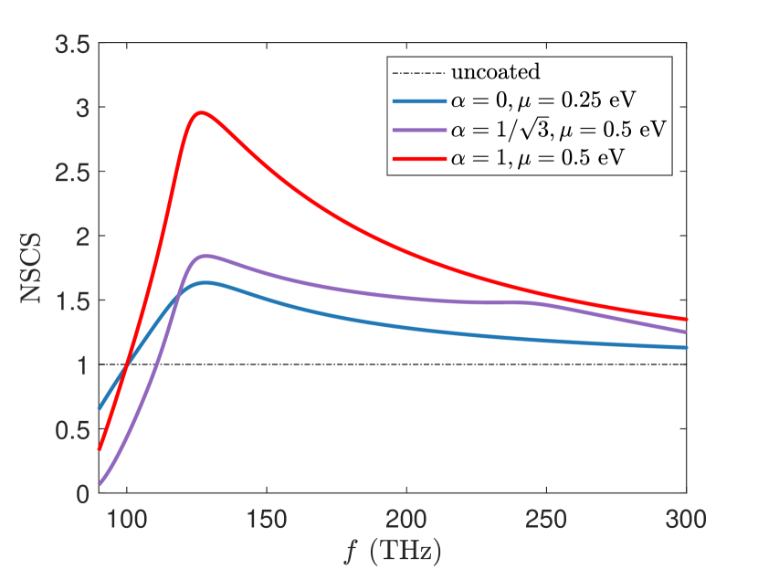
Figure 6 shows NSCS versus frequency for different scattering structures. For a meaningful comparison, we choose the number of layers to be and set the temperature to be K for all structures. Without coating, the value of NSCS is one. For (graphene), when the chemical potential of eV is applied, there is a resonance at THz, which is approximately and corresponds to a TE intrinsic plasmon mode in graphene. For , two resonance peaks arise but their strength is weak, which correspond to the two different band transition processes. Similar to the multiple frequency phenomenon associated with propagating wave, the resonances are temperature-dependent. For , we double the chemical potential for comparing with the case of graphene, which results in a resonance at the same frequency. The resonance for can be attributed to the flat-band-to-cone transition, which is strong due to the large imaginary part of the conductivity.
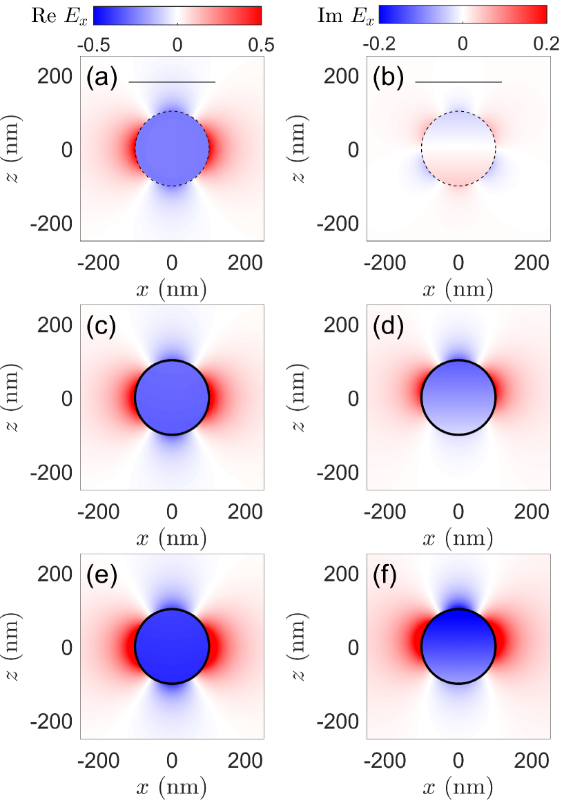
Figure 7 shows the scattering field for THz, corresponding to the left resonant peak in Fig. 6, for three cases: without coating, graphene coating, and pseudospin-1 lattice coating. Without coating, as shown in Figs. 7(a) and 7(b), the scattering field is weak because the wavelength is much larger than the dimension of the scatterer. Figures 7(c) and 7(d) are for with the same parameter setting as in Fig. 6. The scattering field for is shown in Figs. 7(e) and 7(f), demonstrating that the field is enhanced as compared with the case of graphene and greatly enhanced as compared with the case without coating.
V Discussion
Two-dimensional Dirac materials with a flat band have become an active frontier in condensed matter physics and materials science, and it is of interest to understand the optical responses of these materials. In this regard, the basic physical quantity is the optical conductivity. Previous studies focused on the real part of the conductivity. Utilizing - lattice as a vehicle, we have derived a complete formula for the optical conductivity which includes both the real and imaginary parts. The base of our derivation is the Kubo formula and we have also exploited the Kramers–Kronig relation to provide an alternative derivation that leads to the same conductivity formula. Physically, the presence of a flat band, together with the Dirac cone pairs, gives rise to richer transitions as compared with Dirac materials without a flat band, such as graphene. We have demonstrated that the conductivity of - lattice has three components, each contributed to by a distinct optical transition. Specifically, the contribution from intraband transitions is similar to that for Dirac materials without a flat band. While the cone-to-cone transition is pronounced for (graphene), it weakens as increases towards one. For , the flat-band-to-cone transition is dominant. For where the influences of the flat band are the strongest possible, the contribution to the conductivity from the cone-to-cone transition becomes negligible as compared with that from the flat-band-to-cone transition.
With the derived frequency-dependent conductivity formula for - lattice, we have investigated two problems that are fundamental for developing - based optical devices. The first is electromagnetic wave propagation, which results in intrinsic plasmon modes in the - lattice, whose physical properties depend on the polarization. Our calculations have revealed that TM polarized waves are the result of intraband transitions, which occur in the frequency range 1–10 THz. These waves also arise in other 2D Dirac materials such as graphene. In contrast, TE polarized waves are generated by interband transitions, which arise in a higher frequency range: 100–300 THz. For , two interband transitions occur simultaneously, which generate two TE surface waves at , respectively. This is verified by calculating the loss and attenuation length that are minimized in the frequency region. The second problem is scattering from a dielectric sphere coated with multiple layers of - material. The finding is that, due to a reduction in the imaginary part of the optical conductivity at finite temperatures, the scattering of TE polarized waves is weaker than that of TM waves. The multilayer scattering structure can then be used to enhance certain polarization [71, 84, 95].
For 2D Dirac materials, an approach to generating scattering or transport behaviors at multiple frequencies is to use some structure with a special band, such as bilayer graphene with four bands [85]. For a proper choice of the chemical potential, the phenomenon of frequency doubling can occur. In materials similar to graphene such as silicene [93], the sublattice and valley symmetries are broken, thereby generating multiple energy bands. For these materials, the electromagnetic property depends on the chemical potential, so the intrinsic plasmon modes depend on the chemical potential as well. The frequency tunability of these materials is typically weaker than that of - materials for . Recently there is a growing interest in hexagonal boron nitride (hBN) materials [95] whose hyperbolic permittivity can lead to a multi-frequency resonant scattering. However, for the TE polarization in this material, the resonant frequency is fixed. In contrast, our study here has demonstrated that, for the - lattice, insofar as the linear dispersion holds, TE polarized waves can be tuned by adjusting the chemical potential,
A general result is that the optical responses of - materials for are in general more pronounced than those for , e.g., graphene, as the conductivity due to the flat-band-to-cone transition is twice of that due to the cone-to-cone transition. For the same frequency, this means that for pseudospin-1 materials, the chemical potential is effectively doubled, making the optical responses twice as strong as those for graphene. A physical reason for this enhancement is that the plane wave in the pseudospin-1 lattice has a smaller attenuation length due to the large imaginary part of the optical conductivity as compared to that in graphene. From the point of view of resonant scattering, at the same frequency, a larger scattering cross section can arise in pseudospin-1 materials in comparison with graphene. We note that hBN materials can also generate stronger surface plasmon waves than graphene [83, 84].
When performing the scattering calculation for a multilayer - structure, we ignored the effect of interlayer coupling. This approximation can be justified, as follows. In a study of the optical conductivity in monolayer and double-layer - lattice [133], it was observed that the coupling decays exponentially with the interlayer spacing. The results on the plasmon density indicate that only for small layer spacing will the original peak split into two distinct peaks. For reasonably large spacing, e.g., , the layer coupling effect can be neglected.
An extensively studied case is graphene, where monolayer graphene has two linear bands. The bilayer graphene system studied in Refs. [65, 85] has four bands due to interlayer coupling and, as a result, there is splitting in the plasmon peaks. However, when the interlayer distance is large, the coupling effect becomes negligible. For and eV, this critical spacing is about nm. In experiments, stacking geometry is often used to generate multilayer graphene system, where the interlayer coupling effect is insignificant and the electronic structure of the system is similar to that of monolayer graphene [71].
We remark on the possible many-body effects. In graphene, the long-range Coulomb interaction can lead to a renormalized Fermi velocity for and . In Ref. [134], a Hartree-Fock theory was developed with no fitting parameters but with a topological invariant. A theoretical calculation of the Fermi velocity renormalization agreed with the experimental data. While the renormalization can change the optical conductivity, the effect is small.
In Ref. [135], a similar renormalization effect was observed in lattices with a flat band. For and a partially filled flat band, the Drude weight has several zeros depending on the inverse ratio of the band filling. Since the intraband conductivity is proportional to the Drude weight, such a change may also lead to conductivity oscillations for and small . Our work focuses on the case of a positive chemical potential , where the renormalization effect is small.
Can the flat band contribute to the intraband conductivity? In a previous work [136], the authors considered a lattice model with a flat band in the presence of correlated disorders that provide coupling between the flat-band and dispersion band states. For a finite lattice and an initial Gaussian wave packet in the real space, some states in the flat band are unoccupied, giving rise to intraband transitions within the flat band. In our study, correlated disorders were assumed to be absent and the Fermi energy is positive so that the flat band is fully occupied for . Since only the states near the Fermi surface are excited, the flat band gives no contribution to the intraband conductivity. The same observation was made in another previous study [99], where the real part of the conductivity was derived with the finding that the intraband conductivity does not depend on .
With regard to impurity scattering, previously the imaginary part of conductivity was studied in the low frequency regime [111, 112, 113]. It was found that the relaxation time has a significant effect on the convergence of the conductivity. For a small impurity scattering rate, the imaginary part tends to diverge for near zero frequency. The values of the relaxation time for flat-band Dirac materials are not known at the present. However, our study focuses on the physically more relevant high frequency regime.
To summarize, the analysis of our complete formula of the optical conductivity for - suggest a number of phenomena that can be useful for designing optical devices based on this type of generalized 2D Dirac materials. For example, for , because of the coexistence of cone-to-cone and flat-band-to-cone transitions, the corresponding lattice can be exploited for TE wave based broad-band devices. Another phenomenon is that the magnitude of the optical conductivity of pseudospin-1 materials is twice as large as that of graphene due to a reduction in the energy required for a flat-band-to-cone transition. A strong TE wave can then be generated and sustain at , giving the possibility to design optical devices using - ribbon or other coupling structures [74, 127, 137]. Recent work in quantum plasmonics has suggested that edge states in graphene can lead to a blue shift in the plasmon modes [138]. It would be interesting to exploit - materials for applications in quantum plasmonics.
Acknowledgement
This work was supported by AFOSR under Grant No. FA9550-21-1-0186.
Appendix A Optical matrix for - lattice
In the tight-binding framework, the low energy excitations in the - lattice are described by the Hamiltonian (1). Associated with the first valley (), there are three bands: , corresponding to the flat band, conduction and valence bands, respectively. The eigenfunctions are
| (18) |
and
| (19) |
where and is the angle of in the polar coordinates. For the second valley, we have , so the solutions can be obtained from a sign change: . Because of the mirror symmetry in the integration with respect to , the minus sign will not change the results.
The optical matrix elements associated with the current operator in the direction are given by
| (20) |
Appendix B Optical conductivity of - lattice
B.1 Derivation based on the Kubo formula
With the Kubo formula (3), the summation over different states can be simplified to the summation from , which corresponds to the direct optical transition. There are three types of band transitions.
Intraband transition.
The transition is from the conduction band to itself with and . Under the approximations, the Fermi-Dirac distribution can be written as
| (21) |
Equation (3) then becomes
| (22) |
Inserting the optical matrix elements into Eq. (20) and using the linear dispersion relationship , in the polar coordinates we have
| (23) |
Equation (22) becomes
| (24) |
Introducing , we obtain the intraband conductivity as
| (25) |
Cone-to-cone transition.
This transition occurs from to and vice visa. Due to the involvement of two different bands, an additional factor of arises in the summation;
| (26) |
Since and because and belong to different bands, we can write and . Using the integral in Eq. (23) and the optical matrix elements Eq. (20), we get
| (27) |
The difference in the Fermi-Dirac distribution from the case of intraband transition implies that a non-zero value occurs only for or , so in the polar coordinates only the first term is meaningful. We obtain
| (28) |
This integral has a singularity for . Using the residue theorem, we get
| (29) |
where is the Heaviside step function. It can be verified that, for , Eq. (29) reduces to the formula for graphene. For , the integral is zero, indicating that for the pseudospin-1 lattice, the cone-to-cone transition has no contribution to the optical conductivity.
Flat-band-to-cone transition.
The derivation of the contribution to the optical conductivity by the flat-band-to-cone transition is similar to that with the cone-to-cone transition. In particular, for the flat-band-to-cone transition, we have and , so
| (30) |
The singularity now occurs at with the weight . Evaluating this integral, we get
| (31) |
B.2 Derivation based on Kramers-Kronig formula
As proposed in Ref. [88], a different approach to deriving the optical conductivity is to calculate the real part first and then use the Kramers-Kronig formula to obtain the imaginary part. We express the conductivity as the sum of a “normal” term and a term containing a -singularity
| (32) |
where is the Drude weight (or charge stiffness, to be defined below). To obtain the real part of the “normal” term, we use
| (33) |
First, we consider the cone-to-cone transition where , , and the band degeneracy is two. We have
| (34) |
The difference in the Fermi-Dirac functions is one only for , and the function is contained in the integration region for . We thus have a step transition at :
| (35) |
Similarly, we obtain, for the flat-band-to-cone transition, the real part of the conductivity:
| (36) |
which is consistent with the result in Ref. [97].
To calculate the imaginary part of the conductivity, we use the Kramers–Kronig (KK) formula [139], which connects the real and imaginary parts of the response function. There is an additional term in the integral, which is determined by a cutoff in the case of twisted bilayer graphene [88]. The method consists of three steps.
Step 1: Calculate the maximum of Re for :
| (37) |
Step 2: Define the Drude weight (or charge stiffness) as
| (38) |
Step 3: Use the Kramers-Kronig relation to write the imaginary part of the conductivity as
| (39) |
For the - lattice, we have
so the Drude weight is
| (40) |
and the Kramers-Kronig relation becomes
| (41) |
Together with the real part in Eqs. (35) and (36) as well as the imaginary part Eq. (41), we obtain the same conductivity formulas as these derived based on the Kubo formula [Eqs. (25), (29), and (31)].
B.3 Effects of finite temperatures on optical conductivity in the - lattice
Consider graphene at a finite temperature, where the Fermi-Dirac distribution can no longer be treated as a step function. Previous work [140] gives
| (42) |
Comparing Eqs. (29) and (31) as well as the Fermi-Dirac distribution, we can eliminate the factor of in Eq. (42) and study the effects of finite temperature on the flat-band-to-cone transition through the transformations:
| (43) |
B.4 Effects of impurity scattering on optical conductivity in the - lattice
When impurity scattering occurs, a Drude peak will arise in the intra-band component of the conductivity. For graphene, a previous work [64] revealed that the Drude peak gives a singularity at of the form . Here we derive the corresponding formula for - lattice.
Considering the intraband conductivity as given by Eq. (4) and making the change with being the relaxation time, we get
| (44) |
Introducing , we have
| (45) |
Taking two successive limits: first and then , leads to the Drude peak
| (46) |
Together with Eq. (25), we get Eq. (4) in the main text. This result can be verified by inserting the Drude weight into Eq. (32).
The above derivation can be justified, as follows. First, the result depends strongly on the order of limit taking. Note that the Drude singularity is represented by a -function with a coefficient proportional to the chemical potential . However, the function is not properly defined for . For graphene in the continuum limit, we have and , where the conductivity reaches minimum at the Dirac point but the minimal value remains unresolved [116]. Taking the two limits in the opposite order will generate a different result. Nevertheless, for optical waves in graphene, because of their high frequency, a positive Fermi energy is required.
Second, the Drude singularity does not depend on , which is consistent with the result in Ref. [99]. That is, for different values of , the intraband conductivity is invariant. Note that, however, the experimental value of the relaxation time for the - lattice is currently unavailable.
Third, for finite impurity scattering, the following substitution holds:
| (47) |
About the choice of , in Ref. [115], the authors suggested s. The corresponding conductivity is plotted in Figs. 5(a) and 5(b), which reveal that the effect of the impurity on the conductivity arises only at low frequencies. Heuristically, this is because, in graphene, is of the magnitude s (corresponding approximately to THz), but optical processes in graphene typically occur in the frequency regime above this value. As a result, taking into account impurity scattering will not change our result appreciably.
We note that an alternative approach to obtaining the Drude singularity was provided in Ref. [88], in which the authors separated the conductivity into two components: a regular component and a term containing a -singularity:
| (48) |
where has been derived in Appendix B2 and is the Drude weight. Substituting the formula of derived in Appendix B2 into the equation leads to the same result.
B.5 Imaginary part of the optical conductivity in the low frequency regime and the effects of impurity scattering
We study the optical conductivity of the - lattice in the small frequency regime. To this end, an earlier work considered the imaginary part of the optical conductivity in superconducting materials in the zero frequency limit [111, 112], where the results were presented in terms of the product of the frequency and the imaginary part of the conductivity, which is related to the inverse square of the penetrate depth [111, 112, 113] as
The results indicated that, for a low impurity scattering rate, the quantity Im can maintain a finite value for a larger frequency interval near zero. As the impurity scattering rate decreases, the imaginary part of the conductivity diverges. Physically, this means that the superconducting materials could have a divergent imaginary part of the conductivity. On the contrary, for normal states, the quantity Im decays quickly to zero and thus converges.
For an - lattice, the two interband transitions as described by Eqs. (29) and (31) vanish at the low frequency limit, since a low energy photon is not able to induce an interband transition. For a finite Fermi energy, impurity scattering does not change this picture. For the intraband transition in the presence of an impurity, roughly there are two regimes in Eq. (44). In the first regime, decreasing the frequency will increase the driving period but it is still smaller than the relaxation time associated with impurity scattering. In this case, it can be seen from Eq. (44) that the product Im converges to a quantity proportional to the chemical potential. The second regime is where the frequency decreases further so that the driving period is longer than the impurity scattering relaxation time. In this case, impurity scattering dominates and the imaginary part of the optical conductivity approaches zero.
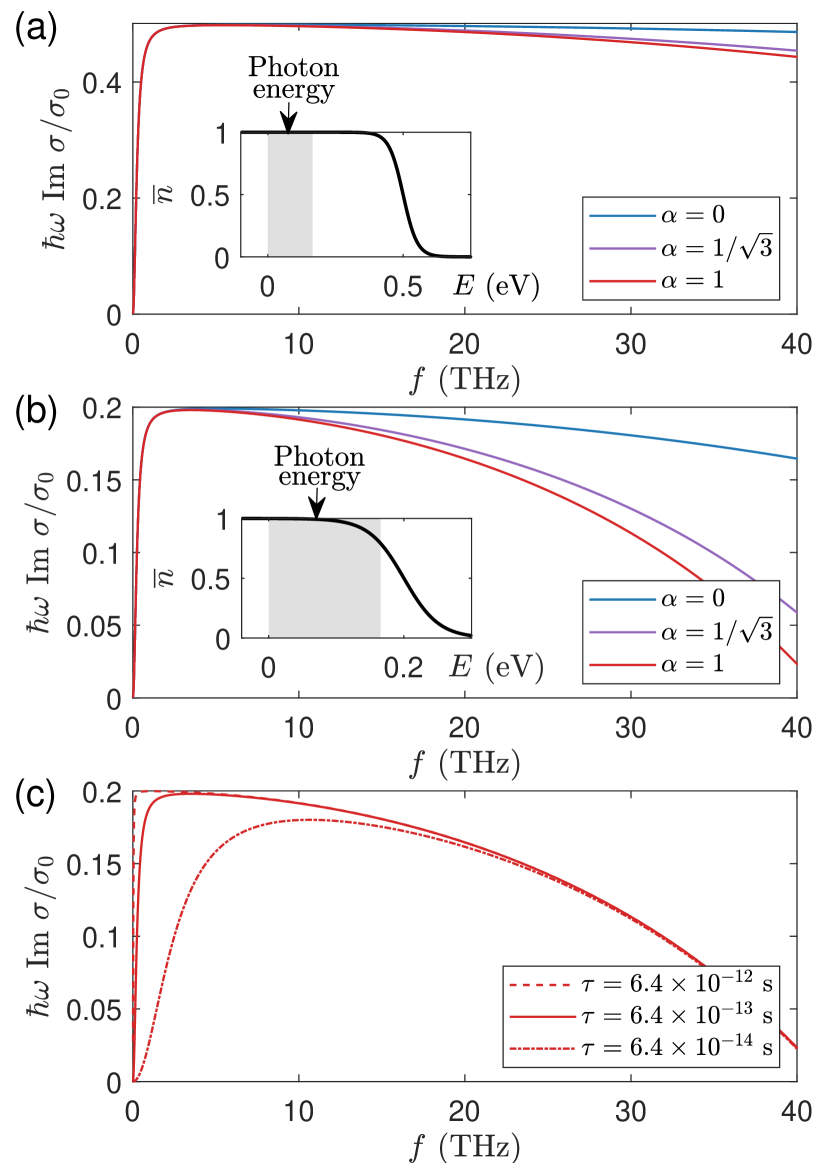
Figure 8(a) shows versus the frequency for , and 1, where the temperature is K and the chemical potential is eV. In this frequency range, the corresponding photon energy lies in the interval as indicated by the shaded region in the inset. We see that the functional behavior of versus is similar for the three different values of . Since the imaginary part of the optical conductivity plays an important role in surface wave prorogation and scattering, the physical significance is that the flat band has little effect on these processes. In this case, the flat band () states are full, but any photon energy in the shaded region in Fig. 8(a) is not sufficient to generate an interband transition. Since the flat band plays no rule in the optical transitions, different values of will lead to the same optical conductivity.
As the Fermi energy is reduced to, e.g., eV, differences in the functional behavior of versus begin to emerge, as shown in Fig. 8(b). From the Fermi-Dirac distribution in the inset, we see that the photon energy is now sufficient to generate interband transitions. In this case, the flat band will affect the behavior of , but the effect is reduced for small frequencies. Increasing the temperature will result in a similar effect.
Figure 8(c) shows versus for three values of the relaxation time of impurity scattering. For relatively large values of (e.g., s or s), the quantity approximately attains the value of the chemical potential in the low frequency regime before decreasing to zero as the frequency increases. As the value of decreases (e.g., to s), impurity scattering begins to dominate, leading to an appreciable change in the functional behavior of versus . We note that this effect of impurity scattering on the optical conductivity was previously observed [111].
The results in Fig. 8 can be concisely summarized, as follows.
-
•
For fixed impurity scattering rate and Fermi energy, as decreases, the product Im first reaches some value proportional to the chemical potential and then attains a different (but convergent) value after impurity scattering dominates.
-
•
For fixed impurity scattering rate and frequency , the value of Im depends on for a small Fermi energy due to the enhanced interband transition.
-
•
For fixed value of and Fermi energy, a small impurity scattering rate (equivalently, a large relaxation time) will lead to divergence of Im. However, for some time that satisfies , the impurity scattering dominates. In this case, the conductivity is convergent.
Appendix C Scattering cross section from a multilayer sphere
To numerically calculate the scattering cross section, we use the iterative method in Ref. [132]. Here we present the key formulas.
Consider a spherical structure of layers, where the core is labeled as and the region outside the structure is denoted as . In each layer, the radius is and the refractive index is . Define
| (49) |
where and are the spherical Bessel functions of the first and third kind, respectively. Consider the following quantities
where the coefficients and are to be calculated. Matching the boundary conditions for each layer leads to the following iterative equations:
We start from and iterate the above equations until the final layer is reached. In our computation, the parameter values are and nm for PTFE, and nm for - lattice, and for free space. The scattering cross section is given by
| (50) |
References
- Sutherland [1986] B. Sutherland, Localization of electronic wave functions due to local topology, Phys. Rev. B 34, 5208 (1986).
- Bercioux et al. [2009] D. Bercioux, D. Urban, H. Grabert, and W. Häusler, Massless Dirac-Weyl fermions in a optical lattice, Phys. Rev. A 80, 063603 (2009).
- Shen et al. [2010] R. Shen, L. B. Shao, B. Wang, and D. Y. Xing, Single Dirac cone with a flat band touching on line-centered-square optical lattices, Phys. Rev. B 81, 041410 (2010).
- Green et al. [2010] D. Green, L. Santos, and C. Chamon, Isolated flat bands and spin-1 conical bands in two-dimensional lattices, Phys. Rev. B 82, 075104 (2010).
- Dóra et al. [2011] B. Dóra, J. Kailasvuori, and R. Moessner, Lattice generalization of the Dirac equation to general spin and the role of the flat band, Phys. Rev. B 84, 195422 (2011).
- Wang and Ran [2011] F. Wang and Y. Ran, Nearly flat band with Chern number c=2 on the dice lattice, Phys. Rev. B 84, 241103 (2011).
- Huang et al. [2011] X. Huang, Y. Lai, Z. H. Hang, H. Zheng, and C. T. Chan, Dirac cones induced by accidental degeneracy in photonic crystals and zero-refractive-index materials, Nat. Mater. 10, 582 (2011).
- Mei et al. [2012] J. Mei, Y. Wu, C. T. Chan, and Z.-Q. Zhang, First-principles study of Dirac and Dirac-like cones in phononic and photonic crystals, Phys. Rev. B 86, 035141 (2012).
- Moitra et al. [2013] P. Moitra, Y. Yang, Z. Anderson, I. I. Kravchenko, D. P. Briggs, and J. Valentine, Realization of an all-dielectric zero-index optical metamaterial, Nat. Photon. 7, 791 (2013).
- Raoux et al. [2014] A. Raoux, M. Morigi, J.-N. Fuchs, F. Piéchon, and G. Montambaux, From dia-to paramagnetic orbital susceptibility of massless fermions, Phys. Rev. Lett. 112, 026402 (2014).
- Guzmán-Silva et al. [2014] D. Guzmán-Silva, C. Mejía-Cortés, M. A. Bandres, M. C. Rechtsman, S. Weimann, S. Nolte, M. Segev, A. Szameit, and R. A. Vicencio, Experimental observation of bulk and edge transport in photonic Lieb lattices, New J. Phys. 16, 063061 (2014).
- Romhányi et al. [2015] J. Romhányi, K. Penc, and R. Ganesh, Hall effect of triplons in a dimerized quantum magnet, Nat. Commun. 6, 6805 (2015).
- Giovannetti et al. [2015] G. Giovannetti, M. Capone, J. van den Brink, and C. Ortix, Kekulé textures, pseudospin-one Dirac cones, and quadratic band crossings in a graphene-hexagonal indium chalcogenide bilayer, Phys. Rev. B 91, 121417 (2015).
- Li et al. [2015a] Y. Li, S. Kita, P. Muoz, O. Reshef, D. I. Vulis, M. Yin, M. Lonar, and E. Mazur, On-chip zero-index metamaterials, Nat. Photon. 9, 738 (2015a).
- Mukherjee et al. [2015] S. Mukherjee, A. Spracklen, D. Choudhury, N. Goldman, P. Öhberg, E. Andersson, and R. R. Thomson, Observation of a localized flat-band state in a photonic Lieb lattice, Phys. Rev. Lett. 114, 245504 (2015).
- Vicencio et al. [2015] R. A. Vicencio, C. Cantillano, L. Morales-Inostroza, B. Real, C. Mejía-Cortés, S. Weimann, A. Szameit, and M. I. Molina, Observation of localized states in Lieb photonic lattices, Phys. Rev. Lett. 114, 245503 (2015).
- Taie et al. [2015] S. Taie, H. Ozawa, T. Ichinose, T. Nishio, S. Nakajima, and Y. Takahashi, Coherent driving and freezing of bosonic matter wave in an optical Lieb lattice, Sci. Adv. 1, e1500854 (2015).
- Fang et al. [2016] A. Fang, Z. Q. Zhang, S. G. Louie, and C. T. Chan, Klein tunneling and supercollimation of pseudospin-1 electromagnetic waves, Phys. Rev. B 93, 035422 (2016).
- Diebel et al. [2016] F. Diebel, D. Leykam, S. Kroesen, C. Denz, and A. S. Desyatnikov, Conical diffraction and composite Lieb bosons in photonic lattices, Phys. Rev. Lett. 116, 183902 (2016).
- Zhu et al. [2016] L. Zhu, S.-S. Wang, S. Guan, Y. Liu, T. Zhang, G. Chen, and S. A. Yang, Blue phosphorene oxide: Strain-tunable quantum phase transitions and novel 2D emergent fermions, Nano Lett. 16, 6548 (2016).
- Bradlyn et al. [2016] B. Bradlyn, J. Cano, Z. Wang, M. G. Vergniory, C. Felser, R. J. Cava, and B. A. Bernevig, Beyond Dirac and Weyl fermions: Unconventional quasiparticles in conventional crystals, Science 353 (2016).
- Fulga and Stern [2017] I. C. Fulga and A. Stern, Triple point fermions in a minimal symmorphic model, Phys. Rev. B 95, 241116 (2017).
- Ezawa [2017] M. Ezawa, Triplet fermions and Dirac fermions in borophene, Phys. Rev. B 96, 035425 (2017).
- Zhong et al. [2017] C. Zhong, Y. Chen, Z.-M. Yu, Y. Xie, H. Wang, S. A. Yang, and S. Zhang, Three-dimensional pentagon carbon with a genesis of emergent fermions, Nat. Commun. 8, 15641 (2017).
- Zhu et al. [2017] Y.-Q. Zhu, D.-W. Zhang, H. Yan, D.-Y. Xing, and S.-L. Zhu, Emergent pseudospin-1 Maxwell fermions with a threefold degeneracy in optical lattices, Phys. Rev. A 96, 033634 (2017).
- Drost et al. [2017] R. Drost, T. Ojanen, A. Harju, and P. Liljeroth, Topological states in engineered atomic lattices, Nat. Phys. 13, 668 (2017).
- Slot et al. [2017] M. R. Slot, T. S. Gardenier, P. H. Jacobse, G. C. van Miert, S. N. Kempkes, S. J. Zevenhuizen, C. M. Smith, D. Vanmaekelbergh, and I. Swart, Experimental realization and characterization of an electronic Lieb lattice, Nat. Phys. 13, 672 (2017).
- Tan et al. [2018] X. Tan, D.-W. Zhang, Q. Liu, G. Xue, H.-F. Yu, Y.-Q. Zhu, H. Yan, S.-L. Zhu, and Y. Yu, Topological Maxwell metal bands in a superconducting qutrit, Phys. Rev. Lett. 120, 130503 (2018).
- Rizzi et al. [2006] M. Rizzi, V. Cataudella, and R. Fazio, Phase diagram of the Bose-Hubbard model with symmetry, Phys. Rev. B 73, 144511 (2006).
- Burkov and Demler [2006] A. A. Burkov and E. Demler, Vortex-peierls states in optical lattices, Phys. Rev. Lett. 96, 180406 (2006).
- Andrijauskas et al. [2015] T. Andrijauskas, E. Anisimovas, M. Račiūnas, A. Mekys, V. Kudriašov, I. B. Spielman, and G. Juzeliūnas, Three-level Haldane-like model on a dice optical lattice, Phys. Rev. A 92, 033617 (2015).
- Li et al. [2014a] W. Li, M. Guo, G. Zhang, and Y.-W. Zhang, Gapless allotrope possessing both massless Dirac and heavy fermions, Phys. Rev. B 89, 205402 (2014a).
- Novoselov et al. [2005] K. S. Novoselov, A. K. Geim, S. V. Morozov, D. Jiang, M. I. Katsnelson, I. Grigorieva, S. Dubonos, and A. A. Firsov, Two-dimensional gas of massless Dirac fermions in graphene, Nature 438, 197 (2005).
- Zhang et al. [2005] Y. B. Zhang, Y. W. Tan, H. L. Stormer, and P. Kim, Experimental observation of the quantum Hall effect and Berry’s phase in graphene, Nature (London) 438, 201 (2005).
- Urban et al. [2011] D. F. Urban, D. Bercioux, M. Wimmer, and W. Häusler, Barrier transmission of Dirac-like pseudospin-one particles, Phys. Rev. B 84, 115136 (2011).
- Xu and Lai [2016] H.-Y. Xu and Y.-C. Lai, Revival resonant scattering, perfect caustics, and isotropic transport of pseudospin-1 particles, Phys. Rev. B 94, 165405 (2016).
- Vigh et al. [2013] M. Vigh, L. Oroszlány, S. Vajna, P. San-Jose, G. Dávid, J. Cserti, and B. Dóra, Diverging dc conductivity due to a flat band in a disordered system of pseudospin-1 Dirac-Weyl fermions, Phys. Rev. B 88, 161413 (2013).
- Chalker et al. [2010] J. T. Chalker, T. S. Pickles, and P. Shukla, Anderson localization in tight-binding models with flat bands, Phys. Rev. B 82, 104209 (2010).
- Bodyfelt et al. [2014] J. D. Bodyfelt, D. Leykam, C. Danieli, X. Yu, and S. Flach, Flatbands under correlated perturbations, Phys. Rev. Lett. 113, 236403 (2014).
- Lieb [1989] E. H. Lieb, Two theorems on the Hubbard model, Phys. Rev. Lett. 62, 1201 (1989).
- Tasaki [1992] H. Tasaki, Ferromagnetism in the Hubbard models with degenerate single-electron ground states, Phys. Rev. Lett. 69, 1608 (1992).
- Aoki et al. [1996] H. Aoki, M. Ando, and H. Matsumura, Hofstadter butterflies for flat bands, Phys. Rev. B 54, R17296 (1996).
- Weeks and Franz [2010] C. Weeks and M. Franz, Topological insulators on the Lieb and perovskite lattices, Phys. Rev. B 82, 085310 (2010).
- Goldman et al. [2011] N. Goldman, D. F. Urban, and D. Bercioux, Topological phases for fermionic cold atoms on the Lieb lattice, Phys. Rev. A 83, 063601 (2011).
- Vidal et al. [1998] J. Vidal, R. Mosseri, and B. Douçot, Aharonov-Bohm cages in two-dimensional structures, Phys. Rev. Lett. 81, 5888 (1998).
- Xu and Lai [2017] H. Xu and Y.-C. Lai, Superscattering of a pseudospin-1 wave in a photonic lattice, Phys. Rev. A 95, 012119 (2017).
- Xu et al. [2017] H.-Y. Xu, L. Huang, D. Huang, and Y.-C. Lai, Geometric valley Hall effect and valley filtering through a singular Berry flux, Phys. Rev. B 96, 045412 (2017).
- Wang et al. [2019] C.-Z. Wang, C.-D. Han, H.-Y. Xu, and Y.-C. Lai, Chaos-based Berry phase detector, Phys. Rev. B 99, 144302 (2019).
- Han et al. [2019] C.-D. Han, H.-Y. Xu, D. Huang, and Y.-C. Lai, Atomic collapse in pseudospin-1 systems, Phys. Rev. B 99, 245413 (2019).
- Xu and Lai [2020a] H.-Y. Xu and Y.-C. Lai, Anomalous chiral edge states in spin-1 Dirac quantum dots, Phys. Rev. Research 2, 013062 (2020a).
- Xu and Lai [2020b] H.-Y. Xu and Y.-C. Lai, Anomalous in-gap edge states in two-dimensional pseudospin-1 Dirac insulators, Phys. Rev. Research 2, 023368 (2020b).
- Xu et al. [2021] H.-Y. Xu, L. Huang, and Y.-C. Lai, Klein scattering of spin-1 Dirac-Weyl wave and localized surface plasmon, Phys. Rev. Research 3, 013284 (2021).
- Han et al. [2020] C.-D. Han, H.-Y. Xu, and Y.-C. Lai, Electrical confinement in a spectrum of two-dimensional Dirac materials with classically integrable, mixed, and chaotic dynamics, Phys. Rev. Research 2, 013116 (2020).
- Cao et al. [2018] Y. Cao, V. Fatemi, S. Fang, K. Watanabe, T. Taniguchi, E. Kaxiras, and P. Jarillo-Herrero, Unconventional superconductivity in magic-angle graphene superlattices, Nature 556, 43 (2018).
- Yankowitz et al. [2019] M. Yankowitz, S. Chen, H. Polshyn, Y. Zhang, K. Watanabe, T. Taniguchi, D. Graf, A. F. Young, and C. R. Dean, Tuning superconductivity in twisted bilayer graphene, Science 363, 1059 (2019).
- Sharpe et al. [2019] A. L. Sharpe, E. J. Fox, A. W. Barnard, J. Finney, K. Watanabe, T. Taniguchi, M. A. Kastner, and D. Goldhaber-Gordon, Emergent ferromagnetism near three-quarters filling in twisted bilayer graphene, Science 365, 605 (2019).
- Lu et al. [2019] X.-B. Lu, P. Stepanov, W. Yang, M. Xie, M. A. Aamir, I. Das, C. Urgell, K. Watanabe, T. Taniguchi, G.-Y. Zhang, A. Bachtold, A. H. MacDonald, and D. K. Efetov, Superconductors, orbital magnets, and correlated states in magic angle bilayer graphene, Nature 574, 653 (2019).
- Vakil and Engheta [2011] A. Vakil and N. Engheta, Transformation optics using graphene, Science 332, 1291 (2011).
- Grigorenko et al. [2012] A. N. Grigorenko, M. Polini, and K. Novoselov, Graphene plasmonics, Nat. Photon. 6, 749 (2012).
- Bao and Loh [2012] Q. Bao and K. P. Loh, Graphene photonics, plasmonics, and broadband optoelectronic devices, ACS Nano 6, 3677 (2012).
- Ying et al. [2018] L. Ying, L. Huang, and Y.-C. Lai, Enhancing optical response of graphene through stochastic resonance, Phys. Rev. B 97, 144204 (2018).
- Gusynin and Sharapov [2006] V. Gusynin and S. Sharapov, Transport of Dirac quasiparticles in graphene: Hall and optical conductivities, Phys. Rev. B 73, 245411 (2006).
- Falkovsky and Varlamov [2007] L. Falkovsky and A. Varlamov, Space-time dispersion of graphene conductivity, Eur. Phys. J. B 56, 281 (2007).
- Gusynin et al. [2006] V. Gusynin, S. Sharapov, and J. Carbotte, Unusual microwave response of Dirac quasiparticles in graphene, Phys. Rev. Lett. 96, 256802 (2006).
- Abergel and Fal’ko [2007] D. Abergel and V. I. Fal’ko, Optical and magneto-optical far-infrared properties of bilayer graphene, Phys. Rev. B 75, 155430 (2007).
- Mikhailov and Ziegler [2007] S. A. Mikhailov and K. Ziegler, New electromagnetic mode in graphene, Phys. Rev. Lett. 99, 016803 (2007).
- Hanson [2008] G. W. Hanson, Dyadic Green’s functions and guided surface waves for a surface conductivity model of graphene, J. Appl. Phys. 103, 064302 (2008).
- Li et al. [2008] Z. Li, E. A. Henriksen, Z. Jiang, Z. Hao, M. C. Martin, P. Kim, H. Stormer, and D. N. Basov, Dirac charge dynamics in graphene by infrared spectroscopy, Nat. Phys. 4, 532 (2008).
- Kuzmenko et al. [2008] A. B. Kuzmenko, E. Van Heumen, F. Carbone, and D. Van Der Marel, Universal optical conductance of graphite, Phys. Rev. Lett. 100, 117401 (2008).
- Mak et al. [2008] K. F. Mak, M. Y. Sfeir, Y. Wu, C. H. Lui, J. A. Misewich, and T. F. Heinz, Measurement of the optical conductivity of graphene, Phys. Rev. Lett. 101, 196405 (2008).
- Bao et al. [2011] Q. Bao, H. Zhang, B. Wang, Z. Ni, C. H. Y. X. Lim, Y. Wang, D. Y. Tang, and K. P. Loh, Broadband graphene polarizer, Nat. Photonics 5, 411 (2011).
- Li et al. [2014b] W. Li, B. Chen, C. Meng, W. Fang, Y. Xiao, X. Li, Z. Hu, Y. Xu, L. Tong, H. Wang, et al., Ultrafast all-optical graphene modulator, Nano Lett. 14, 955 (2014b).
- Ju et al. [2011] L. Ju, B. Geng, J. Horng, C. Girit, M. Martin, Z. Hao, H. A. Bechtel, X. Liang, A. Zettl, Y. R. Shen, et al., Graphene plasmonics for tunable terahertz metamaterials, Nat. Nanotechnol. 6, 630 (2011).
- Nikitin et al. [2011] A. Y. Nikitin, F. Guinea, F. García-Vidal, and L. Martín-Moreno, Edge and waveguide terahertz surface plasmon modes in graphene microribbons, Phys. Rev. B 84, 161407 (2011).
- Akyildiz et al. [2014] I. F. Akyildiz, J. M. Jornet, and C. Han, Terahertz band: Next frontier for wireless communications, Phys. Commun. 12, 16 (2014).
- Chen and Alu [2011] P.-Y. Chen and A. Alu, Atomically thin surface cloak using graphene monolayers, ACS Nano 5, 5855 (2011).
- Li et al. [2015b] R. Li, X. Lin, S. Lin, X. Liu, and H. Chen, Tunable deep-subwavelength superscattering using graphene monolayers, Opt. Lett. 40, 1651 (2015b).
- Qian et al. [2019] C. Qian, X. Lin, Y. Yang, X. Xiong, H. Wang, E. Li, I. Kaminer, B. Zhang, and H. Chen, Experimental observation of superscattering, Phys. Rev. Lett. 122, 063901 (2019).
- Lu et al. [2014] L. Lu, J. D. Joannopoulos, and M. Soljačić, Topological photonics, Nat. Photon. 8, 821 (2014).
- Ozawa et al. [2019] T. Ozawa, H. M. Price, A. Amo, N. Goldman, M. Hafezi, L. Lu, M. C. Rechtsman, D. Schuster, J. Simon, O. Zilberberg, et al., Topological photonics, Rev. Mod. Phys. 91, 015006 (2019).
- Harari et al. [2018] G. Harari, M. A. Bandres, Y. Lumer, M. C. Rechtsman, Y. D. Chong, M. Khajavikhan, D. N. Christodoulides, and M. Segev, Topological insulator laser: theory, Science 359, eaar4003 (2018).
- Bandres et al. [2018] M. A. Bandres, S. Wittek, G. Harari, M. Parto, J. Ren, M. Segev, D. N. Christodoulides, and M. Khajavikhan, Topological insulator laser: Experiments, Science 359, eaar4005 (2018).
- Woessner et al. [2015] A. Woessner, M. B. Lundeberg, Y. Gao, A. Principi, P. Alonso-González, M. Carrega, K. Watanabe, T. Taniguchi, G. Vignale, M. Polini, et al., Highly confined low-loss plasmons in graphene–boron nitride heterostructures, Nat. Mater. 14, 421 (2015).
- Musa et al. [2017] M. Y. Musa, M. Renuka, X. Lin, R. Li, H. Wang, E. Li, B. Zhang, and H. Chen, Confined transverse electric phonon polaritons in hexagonal boron nitrides, 2D Mater. 5, 015018 (2017).
- Jablan et al. [2011] M. Jablan, H. Buljan, and M. Soljačić, Transverse electric plasmons in bilayer graphene, Opt. Express 19, 11236 (2011).
- Nilsson et al. [2006] J. Nilsson, A. C. Neto, F. Guinea, and N. Peres, Electronic properties of graphene multilayers, Phys. Rev. Lett. 97, 266801 (2006).
- Falkovsky and Pershoguba [2007] L. Falkovsky and S. Pershoguba, Optical far-infrared properties of a graphene monolayer and multilayer, Phys. Rev. B 76, 153410 (2007).
- Stauber et al. [2013] T. Stauber, P. San-Jose, and L. Brey, Optical conductivity, Drude weight and plasmons in twisted graphene bilayers, New J. Phys. 15, 113050 (2013).
- Stauber and Kohler [2016] T. Stauber and H. Kohler, Quasi-flat plasmonic bands in twisted bilayer graphene, Nano Lett. 16, 6844 (2016).
- Stauber et al. [2018] T. Stauber, T. Low, and G. Gómez-Santos, Chiral response of twisted bilayer graphene, Phys. Rev. Lett. 120, 046801 (2018).
- Lin et al. [2020] X. Lin, Z. Liu, T. Stauber, G. Gómez-Santos, F. Gao, H. Chen, B. Zhang, and T. Low, Chiral plasmons with twisted atomic bilayers, Phys. Rev. Lett. 125, 077401 (2020).
- Deng et al. [2020] B. Deng, C. Ma, Q. Wang, S. Yuan, K. Watanabe, T. Taniguchi, F. Zhang, and F. Xia, Strong mid-infrared photoresponse in small-twist-angle bilayer graphene, Nat. Photonics , 1 (2020).
- Ukhtary et al. [2016] M. S. Ukhtary, A. R. Nugraha, E. H. Hasdeo, and R. Saito, Broadband transverse electric surface wave in silicene, Appl. Phys. Lett. 109, 063103 (2016).
- Iorsh et al. [2013] I. V. Iorsh, I. S. Mukhin, I. V. Shadrivov, P. A. Belov, and Y. S. Kivshar, Hyperbolic metamaterials based on multilayer graphene structures, Phys. Rev. B 87, 075416 (2013).
- Qian et al. [2018] C. Qian, X. Lin, Y. Yang, F. Gao, Y. Shen, J. Lopez, I. Kaminer, B. Zhang, E. Li, M. Soljacic, et al., Multifrequency superscattering from subwavelength hyperbolic structures, ACS Photonics 5, 1506 (2018).
- Li and Carbotte [2013] Z. Li and J. Carbotte, Conductivity of Dirac fermions with phonon-induced topological crossover, Phys. Rev. B 88, 195133 (2013).
- Illes et al. [2015] E. Illes, J. Carbotte, and E. Nicol, Hall quantization and optical conductivity evolution with variable Berry phase in the - model, Phys. Rev. B 92, 245410 (2015).
- Louvet et al. [2015] T. Louvet, P. Delplace, A. A. Fedorenko, and D. Carpentier, On the origin of minimal conductivity at a band crossing, Phys. Rev. B 92, 155116 (2015).
- Tabert et al. [2016] C. Tabert, J. Carbotte, and E. Nicol, Optical and transport properties in three-dimensional Dirac and Weyl semimetals, Phys. Rev. B 93, 085426 (2016).
- Kovács et al. [2017] Á. D. Kovács, G. Dávid, B. Dóra, and J. Cserti, Frequency-dependent magneto-optical conductivity in the generalized - model, Phys. Rev. B 95, 035414 (2017).
- Chen et al. [2019] Y.-R. Chen, Y. Xu, J. Wang, J.-F. Liu, and Z. Ma, Enhanced magneto-optical response due to the flat band in nanoribbons made from the - lattice, Phys. Rev. B 99, 045420 (2019).
- Leykam and Flach [2018] D. Leykam and S. Flach, Perspective: Photonic flatbands, APL Photon. 3, 070901 (2018).
- Mukherjee et al. [2018] S. Mukherjee, M. Di Liberto, P. Öhberg, R. R. Thomson, and N. Goldman, Experimental observation of Aharonov-Bohm cages in photonic lattices, Phys. Rev. Lett. 121, 075502 (2018).
- Franchina Vergel et al. [2020] N. A. Franchina Vergel, L. C. Post, D. Sciacca, M. Berthe, F. Vaurette, Y. Lambert, D. Yarekha, D. Troadec, C. Coinon, G. Fleury, et al., Engineering a robust flat band in III–V semiconductor heterostructures, Nano Lett. (2020).
- Leykam et al. [2018] D. Leykam, A. Andreanov, and S. Flach, Artificial flat band systems: from lattice models to experiments, Adv. Phys. X 3, 1473052 (2018).
- Malcolm and Nicol [2015] J. D. Malcolm and E. J. Nicol, Magneto-optics of massless Kane fermions: Role of the flat band and unusual Berry phase, Phys. Rev. B 92, 035118 (2015).
- Teppe et al. [2016] F. Teppe, M. Marcinkiewicz, S. S. Krishtopenko, S. Ruffenach, C. Consejo, A. Kadykov, W. Desrat, D. But, W. Knap, J. Ludwig, et al., Temperature-driven massless Kane fermions in HgCdTe crystals, Nat. Commun. 7, 1 (2016).
- Charnukha et al. [2019] A. Charnukha, A. Sternbach, H. Stinson, R. Schlereth, C. Brüne, L. W. Molenkamp, and D. Basov, Ultrafast nonlocal collective dynamics of Kane plasmon-polaritons in a narrow-gap semiconductor, Sci. Adv. 5, eaau9956 (2019).
- Hubmann et al. [2020] S. Hubmann, G. V. Budkin, M. Otteneder, D. But, D. Sacré, I. Yahniuk, K. Diendorfer, V. V. Bel’kov, D. A. Kozlov, N. N. Mikhailov, S. A. Dvoretsky, V. S. Varavin, V. G. Remesnik, S. A. Tarasenko, W. Knap, and S. D. Ganichev, Symmetry breaking and circular photogalvanic effect in epitaxial films, Phys. Rev. Materials 4, 043607 (2020).
- Voon and Ram-Mohan [1993] L. L. Y. Voon and L. Ram-Mohan, Tight-binding representation of the optical matrix elements: Theory and applications, Phys. Rev. B 47, 15500 (1993).
- Marsiglio et al. [1996] F. Marsiglio, J. P. Carbotte, A. Puchkov, and T. Timusk, Imaginary part of the optical conductivity of , Phys. Rev. B 53, 9433 (1996).
- Jiang et al. [1996] C. Jiang, E. Schachinger, J. P. Carbotte, D. Basov, and T. Timusk, Imaginary part of the infrared conductivity of a superconductor, Phys. Rev. B 54, 1264 (1996).
- Pronin et al. [2001] A. V. Pronin, A. Pimenov, A. Loidl, and S. I. Krasnosvobodtsev, Optical conductivity and penetration depth in , Phys. Rev. Lett. 87, 097003 (2001).
- Novoselov et al. [2004] K. S. Novoselov, A. K. Geim, S. V. Morozov, D. Jiang, Y. Zhang, S. V. Dubonos, I. V. Grigorieva, and A. A. Firsov, Electric field effect in atomically thin carbon films, Science 306, 666 (2004).
- Jablan et al. [2009] M. Jablan, H. Buljan, and M. Soljačić, Plasmonics in graphene at infrared frequencies, Phys. Rev. B 80, 245435 (2009).
- Sarma et al. [2011] S. D. Sarma, S. Adam, E. Hwang, and E. Rossi, Electronic transport in two-dimensional graphene, Rev. Mod. Phys. 83, 407 (2011).
- Stauber et al. [2008] T. Stauber, N. Peres, and A. Geim, Optical conductivity of graphene in the visible region of the spectrum, Phys. Rev. B 78, 085432 (2008).
- Stern [1967] F. Stern, Polarizability of a two-dimensional electron gas, Phys. Rev. Lett. 18, 546 (1967).
- Fal’ko and Khmel’nitskii [1989] V. I. Fal’ko and D. E. Khmel’nitskii, What if a film conductivity exceeds the speed of light?, Zh. Eksp. Teor. Fiz. 95 (1989).
- Danilov et al. [2000] M. Danilov, R. DeVoe, A. Dolgolenko, G. Giannini, G. Gratta, P. Picchi, A. Piepke, F. Pietropaolo, P. Vogel, J. Vuilleumier, et al., Detection of very small neutrino masses in double-beta decay using laser tagging, Phys. Rev. B 480, 12 (2000).
- Del’Haye et al. [2011] P. Del’Haye, T. Herr, E. Gavartin, M. L. Gorodetsky, R. Holzwarth, and T. J. Kippenberg, Octave spanning tunable frequency comb from a microresonator, Phys. Rev. Lett. 107, 063901 (2011).
- Schliesser et al. [2012] A. Schliesser, N. Picqué, and T. W. Hänsch, Mid-infrared frequency combs, Nat. Photon. 6, 440 (2012).
- Miller [2006] D. A. Miller, On perfect cloaking, Opt. Express 14, 12457 (2006).
- Alù and Engheta [2009] A. Alù and N. Engheta, Cloaking a sensor, Phys. Rev. Lett. 102, 233901 (2009).
- Alù and Engheta [2005] A. Alù and N. Engheta, Achieving transparency with plasmonic and metamaterial coatings, Phys. Rev. E 72, 016623 (2005).
- Peurifoy et al. [2018] J. Peurifoy, Y. Shen, L. Jing, Y. Yang, F. Cano-Renteria, B. G. DeLacy, J. D. Joannopoulos, M. Tegmark, and M. Soljačić, Nanophotonic particle simulation and inverse design using artificial neural networks, Sci. Adv. 4, eaar4206 (2018).
- Zhao et al. [2015] B. Zhao, J. Zhao, and Z. Zhang, Resonance enhanced absorption in a graphene monolayer using deep metal gratings, J. Opt. Soc. Ame. B 32, 1176 (2015).
- Farhat et al. [2013] M. Farhat, C. Rockstuhl, and H. Bağcı, A 3D tunable and multi-frequency graphene plasmonic cloak, Opt. Express 21, 12592 (2013).
- Monticone and Alu [2013] F. Monticone and A. Alu, Do cloaked objects really scatter less?, Phys. Rev. X 3, 041005 (2013).
- Ehrlich et al. [1953] P. Ehrlich, L. Amborski, and R. Burton, Dielectric properties of teflon from room temperature to c and from frequencies of to c/s, J. Res. Nat. Bur. Stand 51, 185 (1953).
- Hulst and van de Hulst [1981] H. C. Hulst and H. C. van de Hulst, Light Scattering by Small Particles (Courier Corporation, New York, 1981).
- Johnson [1996] B. Johnson, Light scattering by a multilayer sphere, Appl. Opt. 35, 3286 (1996).
- Iurov et al. [2020] A. Iurov, G. Gumbs, and D. Huang, Many-body effects and optical properties of single and double layer -lattices, J. Phys.: Condens. Matter 32, 415303 (2020).
- Stauber et al. [2017] T. Stauber, P. Parida, M. Trushin, M. V. Ulybyshev, D. L. Boyda, and J. Schliemann, Interacting electrons in graphene: Fermi velocity renormalization and optical response, Phys. Rev. Lett. 118, 266801 (2017).
- Häusler [2015] W. Häusler, Flat-band conductivity properties at long-range coulomb interactions, Phys. Rev. B 91, 041102 (2015).
- Gneiting et al. [2018] C. Gneiting, Z. Li, and F. Nori, Lifetime of flatband states, Phys. Rev. B 98, 134203 (2018).
- Meng et al. [2020] H. Meng, Q. Lin, X. Xue, J. Lian, G. Liu, W. Xu, X. Zhai, Z. Liu, J. Chen, H. Li, et al., Ultrathin multi-band coherent perfect absorber in graphene with high-contrast gratings, Opt. Express 28, 24285 (2020).
- Wedel et al. [2018] K. O. Wedel, N. A. Mortensen, K. S. Thygesen, and M. Wubs, Emergent scale invariance of nonclassical plasmons in graphene nanoribbons, Phys. Rev. B 98, 155412 (2018).
- Economou [2006] E. N. Economou, Green’s Functions in Quantum Physics, Vol. 7 (Springer-Verlag, Berlin, 2006).
- Falkovsky [2008] L. Falkovsky, Optical properties of graphene, J. Phys. Conf. Ser. 129, 012004 (2008).