Reduced Material Loss in Thin-film Lithium Niobate Waveguides
Abstract
Thin-film lithium niobate has shown promise for scalable applications ranging from single-photon sources to high-bandwidth data communication systems. Realization of the next generation high-performance classical and quantum devices, however, requires much lower optical losses than the current state of the art (10 milion). Unfortunately, material limitations of ion-sliced thin film lithium niobate have not been explored, and therefore it is unclear how high quality factor can be achieved in this platform. Here we evaluate the material limited quality factor of thin film lithium niobate photonic platform can be as high as at telecommunication wavelengths, corresponding to a propagation loss of .
Thin-film lithium niobate (TFLN) platform has enabled a myriad of classical and quantum applications zhu2021integrated , many of which crucially rely on low optical loss. For instance, the bandwidth of electro-optic (EO) frequency combs zhang2019broadband and the efficiency of microwave-to-optical transducers Holzgrafe:20 ; McKenna:20 are proportional to the resonator quality factor or (loss rate)-1. Currently the lowest-reported optical loss in ion-sliced TFLN waveguides is 3 dB/m zhang2017monolithic , which compares favorably to many photonic platforms. At the same time, a loss of 0.2 dB/m was measured using whispering gallery mode resonators created by polishing bulk congruent LN ilchenko2004nonlinear . It is currently an open question if TFLN can reach this, and ideally even lower, loss rates. For example, it has been speculated that ion slicing process, used to create TFLN from bulk LN rabiei2004optical , may result in implantation damage that could yield higher optical absorption in TFLN than in polished bulk LN.
Here, we first develop a post-fabrication process based on annealing in O2 atmosphere in order to reduce material absorption rate of TFLN platform, and then we use Kerr-calibrated linear response measurements liu2020high to evaluate . This requires parameters such as the nonlinear refractive index as well as the ratio between the photothermal and Kerr-induced cross-phase modulation (XPM) responses (at bandwidths 10 MHz) of TFLN. These, and other parameters, are determined by performing laser pump-probe measurements on timescales shorter than the response time of deleterious photorefractive (PR) effects in LN jiang2017fast . Using these pump-probe techniques, we determine that the material limited loss in ion-sliced LN is 1.5 dB/m, and demonstrate an annealing process that reduces this to 0.2 dB/m that approaches the limit of the bulk LN.
The micro-rings are fabricated on a -thick x-cut LN thin-film bonded to a -thick layer of thermal oxide on a silicon wafer (NanoLN). Electron-beam lithography followed by physical reactive Ar+ ion etching, with target etch-depth of 300 nm, yields micro-ring resonators of radius and a waveguide top-width of (Fig 1b).
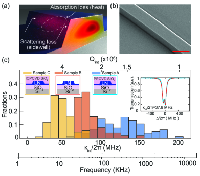
We prepare three sets of resonators from this wafer in the same fabrication run: cladded (Sample-A), annealed (Sample-B), and annealed-cladded-annealed (Sample-C) resonators. Sample-A is fabricated with the process reported in Ref. zhang2017monolithic . That is, the resonators are cladded with an 800 nm-thick layer of SiO2 using plasma-enhanced chemical vapor deposition with substrate temperature of 300C. For Samples-B and -C, the resonators are annealed at atmospheric pressures in O2 at 520C for two hours. The annealing step is used to improve the crystallinity of TFLN, thereby repairing potential damages leidinger2016influence caused by ion slicing han2015optical . We clad Sample-C with a 800 nm-thick layer of SiO2 deposited using inductively coupled plasma chemical vapour deposition (ICPCVD) at 80C, and then re-anneal it under the same conditions.We emphasize the low temperature nature (80C) of ICPCVD process, which we found to be important to maintain the benefits of the annealing step. We measure a mean of , , and million in Samples-A,-B, and -C, respectively (Fig. 1c). We note that all resonances from Samples -B and -C exhibit asymmetric mode splittings due to Rayleigh back-scattering (Fig. 1c).
Before the Kerr-calibrated response measurements, we first determine the timescale of PR effects in the micro-rings since PR-induced resonance frequency change could distort the inferred material response at low modulation frequencies. jiang2017fast . To do this, we optically pump a micro-ring then, after extinguishing the pump, we repeatedly measure one of its resonances with a probe, monitoring the time-dependence of the detuning of the resonance (Fig. 2a). The detuning is normalized to the Kerr shift (discussed later) for convenient comparison. For Sample-A, we observe a blue shift with a time constant of , indicative of PR effects. We did not observe PR behavior for Samples-B and -C over time scales of up to a minute (Fig. 2b). Thus, the PR effect can be ignored for measurements at timescales significantly shorter than 100 s (bandwidths 0.01 Hz).
To calibrate the absorption rate of different devices, we need to evaluate
| (1) |
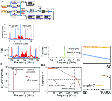
where the optical mode volume, the group index, the effective index, and the photothermal frequency shift gradient at pump frequency , mainly determined by the material thermo-optic coefficients moretti2005temperature and is determined from simulation, see Supplementary materials. The response ratio is the DC offset of the measured response function in Fourier domain, and is obtained through fitting. The material absorption rate also requires a good knowledge of from TFLN. We did an auxiliary pump-probe measurement to obtain for our TFLN, details see Supplementary Material. We did not employ the commonly-used thermal triangle techniquegao2021probing to determine to avoid PR effects.

The measurement of is accomplished by modulating an optical pump and measuring the resultant side-of-fringe modulation of a probe, as induced by the material response of TFLN (see Fig. 3a). The pump modulation frequency is varied to elucidate photothermal and Kerr-induced XPM on the probe, which can be distinguished at low (10 kHz) and high (1 MHz) modulation frequencies, respectively liu2020high . The responses of all the devices were measured, and all yield two plateaus corresponding to either predominantly Kerr induced () or photothermal-induced () responses. The ratios of the plateaus are 11.0, 2.5 and 1.5 for Samples -A, -B, and -C, respectively, indicating that thermal annealing reduces the magnitude of photothermal response. Note that cascaded sum-frequency generation of the pump with the probe will contribute an additional XPM indistinguishable from the Kerr contribution. Given our system parameters, we expect this change to be 10%, see Supplementary materials. For all measurements, the wavelength of the pump is 1550 nm while the probe is at wavelengths detuned several free-spectral ranges of the resonator away. The pump power is kept low () to avoid nonlinearity induced self-feedback.
Finally, using Eq. 1 we calculate to be 8.4 MHz, 1.8 MHz, and 1.1 MHz for Samples -A, -B, and -C, respectively. The absorption rate corresponding to each process is calibrated individually, with Sample-C yielding a material-limited quality factor of ( ) which is among the highest within integrated photonic platforms, see Table 1. Our results suggest that the main source of loss in our high-confinement LN waveguides is line-edge roughness-induced scattering, which limits the average intrinsic quality factor of resonances around to .(Fig. 1c).
| Platform | (pm/V) | () | Q-factor () | |
|---|---|---|---|---|
| SiO2 | 1.45 | 0 | 2.2 | 5363 |
| SiN | 2.0 | 0 | 24 | 287 |
| Ta2O5 | 2.0 | 0 | 62 | 2.64 |
| Al0.2Ga0.8As | 3.3 | 119 | 2600 | 2.04 |
| TFLN (this work) | 2.2 | 30 | 15 | 180 |
In conclusion, we demonstrated that post-fabrication annealing and low-temperature oxide cladding can significantly reduce optical absorption in TFLN waveguides.
Absorption at telecommunication wavelengths is reduced by removing damage potentially caused by ion implantation and reactive-ion etching even at temperatures in which other chemical bonds (e.g. Si-H and O-H) are still present.
Consequently, annealing reduces the material absorption loss significantly over a broad frequency range leidinger2016influence .
Our annealing technique yielded absorption-limited loss on par with 0.2 dB/m measured in bulk LN ilchenko2004nonlinear , corresponding to a material-limited Q-factor of 180 Million.
We anticipate that, by improving TFLN fabrication strategies, -factors approaching the material limit can be achieved, reaching the low-loss regime required for transformative quantum and classical technology,
e.g. deterministic room-temperature single photon source with periodically-poled TFLN micro-ring lu2020toward .
Funding: Air Force Office of Scientific Research (FA9550-19-1-0376), Swiss National Science Foundation (SNSF) (185870, 192293). Defense Advanced Research Projects Agency (HR0011-20-C-0137, HR0011-20-2-0046).
Acknowledgement: We acknowledge fruitful discussions with Martin M. Fejer, Linbo Shao, Maodong Gao, and Christian Reimer. Fabrication is performed at the Harvard University Center for Nanoscale Systems (CNS).
Disclosures: L.H, P.K, M.Z and M.L are involved in developing TFLN technologies at Hyperlight Corporation.
Disclaimer: The views, opinions and/or findings expressed are those of the author and should not be interpreted as representing the official views or policies of the Department of Defense or the U.S. Government.
Supplementary materials
Estimated contribution of cascaded sum-frequency generation to XPM
Determining relies on pump-probe measurements (e.g. the detuning of a resonance with modulating the pump) in our experiment. In this case, cascaded sum-frequency generation (SFG) of the bright pump with the dim probe will contribute to an effective XPM term since the shift of the cavity resonances is measured as a function of pump power rather than probe power. However, for TFLN, owing to its large , cascaded second order nonlinearities can contribute an with nearly equal and opposite sign to the pure electronic of LN. As a result, values of inferred from Z-scans in bulk material or the thermal triangle in ring resonators may differ by an order of magnitude from the real valuePhillips:11 ; Conti:02 . We may estimate the strength of these contributions for the waveguides under consideration here by finding both the nonlinear coupling and phase-mismatch between the pump, probe, and generated sum-frequency.
The coupled wave equations for three-wave mixing are given (in power normalized units) by
| (2a) | |||
| (2b) | |||
| (2c) | |||
where . In the undepleted limit, we may assume that the bright pump is given by , and , where is assumed to be approximately linear in . We assume , in which case the sum frequency is given by
| (3) |
Substituting Eqn 3 into Eqns 2b-2a, we have
| (4a) | |||
| (4b) | |||
where we have ignored oscillatory terms that do not contribute to the average phase accumulated by and . Substituting the approximations , and into Eqns 4b-4a, we find
| (5a) | |||
| (5b) | |||
The cross-phase modulation that occurs during phase-mismatched SFG between the bright pump and dim probe signal is indistinguishable from the XPM typically encountered in media, since both are linear in pump power, and has the opposite sign for typical values of . The scaling associated with cascaded nonlinearities may render the strength of this effect a strong function of waveguide geometry. We also note here that while Eqns 5b-5a are accurate for TM modes in Z-cut thin films, these expressions need to be corrected for TE modes in X-cut thin films. In this case, oscillates periodically during propagation around a ring since the tensor associated with interaction is not invariant with respect to rotations around the crystalline X axis. We further note that typical waveguide geometries in LN exhibit avoided crossings between TE and TM modes for propagation angles offset from the crystalline axes. For large radii rings, these avoided crossings cause a TE-polarized mode to undergo adiabatic conversion between TE and TM, thereby contributing more rapid oscillations to both and . In this more general case, we may Fourier series expand and , and solve Eqns 5b-5a for each Fourier component. The total contribution to the XPM coefficient is given by
| (6) |
where is the th Fourier component of and is the phase-mismatch associated with each Fourier component. For large radii rings , and the total contribution from each component may be evaluated using Parseval’s theorem. Using this approximation and the waveguide geometry shown in main text Fig.1, we estimate that the contribution of cascaded nonlinearities to the net XPM coefficient is below 10%.
n2 calibration method
The material absorption rate requires evaluation of . Since there is no reliable literature on of TFLN, we perform measurements on an auxiliary z-cut sample with similar waveguide geometry to determine . We chose this specific crystal direction to minimize error of the cascaded calculation and mitigate the impact of adiabatic evolution of the modes from TE to TM during propagation in x-cut sample due to birefringence.
Due to the presence of PR effects, commonly-used thermal triangle techniquegao2021probing that uses high optical power to determine is not suitable for our platform. Instead, we use a pump-probe scheme (setup see Fig. 4a) similar to the one used in the main text to determine the value of in TFLN at low optical power. The main idea of this measurement is to carefully calibrate how much pump intracavity power density modulation is applied, and how much probe cavity frequency modulation is induced by Kerr effect, after which the value of can be retrieved through relation
| (7) |
where are the mode intensity weighted average of the corresponding physical quantities, retrieved from simulation.
The intracavity power density modulation is determined by the intensity modulation depth and the waveguide circulating power ,
We intensity modulate the pump intensity at MHz and determine the modulation-depth using heterodyne measurements (Fig. 4b red spectrum), frequency offset by 100 MHz using Acousto-optic modulators. The intracavity power density as a function of waveguide circulating power depends on many parameters. Apart from cavity coupling rates, the power is also affected by the background etalon formed due to the chip facet reflections. Transmission trace thus consists an overall broad background sine modulation, and a Fano-shaped narrow cavity resonance dip. We express the intracavity power density considering all these effects as
with the cavity external coupling rate, the cavity linewdith, the laser detuning, the waveguide background etalon fringe periodicity, the etalon phase offset, the characteristic etalon reflectivity, and the mode volume of the pump mode. Here, power is the waveguide circulating power at the quadrature point of the waveguide background etalon fringe. All the parameters used in the power density function is fitted from the pump mode transmission profile shown in Fig.4d, using fitting function,
Sidebands at are applied to calibrate the laser detuning. The fitting results are shown in the following table:
| 0.152 |
After the intracavity power density function is determined through fitting the cavity transmission trace, we need to calibrate how much Kerr frequency modulation on the probe cavity is induced from a given waveguide circulating power . To calibrate the cavity frequency modulation depths, we use the method from Ref gorodetksy2010determination by comparing the Kerr frequency modulation signal to a reference phase modulation with known depth (calibrated also using heterodyne measurements, Fig. 4b blue spectrum). The phase modulation is applied to the probe laser at , and is visible in Fig. 4c right next to the cavity frequency modulation signal at . The reference phase modulation acts as a ruler and allows us to compare and retrieve the cavity frequency modulation depth at different optical powers. To isolate the cavity frequency modulation contributed by Kerr effect from the one from thermal effect, we also measured the XPM response at different pump modulation frequencies using a vector network analyzer. We retrieved the fraction of pure Kerr contribution to the total XPM signal at MHz by fitting the measured response (Fig. 4e). After that, the Kerr induced cavity frequency modulation can be expressed as
where is the power spectral density ratio between the reference phase modulation signal and the XPM total signal measured on the real-time spectrum analyzer.
Since we do not have direct access to the on-chip waveguide circulating power, and the coupling efficiencies at the chip facets can be different, we mitigate the uncertainties by taking the geometry average of the input power and output power of the chip as the waveguide circulating power , measured at the etalon quadrature point. We measure the XPM ratio at the given setting, and repeat the measurement (measure ratio ) after reversing the input and output of the micro-ring, in order to take into account different coupling efficiencies at the chip facets. The spectrum when measuring both and are shown in Fig. 4c, and we take their geometric average as well .
For all measurements, the wavelength of the pump is 1550 nm while the probe is at wavelengths detuned several free-spectral ranges of the resonator away. The pump power is kept low () to avoid nonlinearity induced self-feedback. With all relevant parameters measured/fitted, by inverting Eq.7, our measurements allow calibrating using
| (8) |
and we find a material nonlinear refractive index of for our TFLN.
Note that cascaded sum-frequency generation of the pump with the probe will contribute an additional XPM indistinguishable from the Kerr contribution. Given our system parameters, we expect this change to be 10%.
All the physical quantities measured/fitted for the calibration are shown in the following table:
| parameters | values |
|---|---|
| 0.1619 | |
| 0.1245 | |
| 0.60 | |
| 44.07 | |
| 1.915 | |
and the other parameters used in either the calibration or the absorption calibration are retrieved from COMSOL simulation, shown in the following table:
| parameters | values |
|---|---|
| 4.53 | |
| abs parameters | values |
| cladded | |
| uncladded |

References
- (1) D. Zhu, L. Shao, M. Yu, R. Cheng, B. Desiatov, C. Xin, Y. Hu, J. Holzgrafe, S. Ghosh, A. Shams-Ansari, et al., “Integrated photonics on thin-film lithium niobate,” Advances in Optics and Photonics, vol. 13, no. 2, pp. 242–352, 2021.
- (2) M. Zhang, B. Buscaino, C. Wang, A. Shams-Ansari, C. Reimer, R. Zhu, J. M. Kahn, and M. Lončar, “Broadband electro-optic frequency comb generation in a lithium niobate microring resonator,” Nature, vol. 568, no. 7752, pp. 373–377, 2019.
- (3) J. Holzgrafe, N. Sinclair, D. Zhu, A. Shams-Ansari, M. Colangelo, Y. Hu, M. Zhang, K. K. Berggren, and M. Lončar, “Cavity electro-optics in thin-film lithium niobate for efficient microwave-to-optical transduction,” Optica, vol. 7, pp. 1714–1720, Dec 2020.
- (4) T. P. McKenna, J. D. Witmer, R. N. Patel, W. Jiang, R. V. Laer, P. Arrangoiz-Arriola, E. A. Wollack, J. F. Herrmann, and A. H. Safavi-Naeini, “Cryogenic microwave-to-optical conversion using a triply resonant lithium-niobate-on-sapphire transducer,” Optica, vol. 7, pp. 1737–1745, Dec 2020.
- (5) M. Zhang, C. Wang, R. Cheng, A. Shams-Ansari, and M. Lončar, “Monolithic ultra-high-q lithium niobate microring resonator,” Optica, vol. 4, no. 12, pp. 1536–1537, 2017.
- (6) V. S. Ilchenko, A. A. Savchenkov, A. B. Matsko, and L. Maleki, “Nonlinear optics and crystalline whispering gallery mode cavities,” Physical review letters, vol. 92, no. 4, p. 043903, 2004.
- (7) P. Rabiei and P. Gunter, “Optical and electro-optical properties of submicrometer lithium niobate slab waveguides prepared by crystal ion slicing and wafer bonding,” Applied Physics Letters, vol. 85, no. 20, pp. 4603–4605, 2004.
- (8) J. Liu, G. Huang, R. N. Wang, J. He, A. S. Raja, T. Liu, N. J. Engelsen, and T. J. Kippenberg, “High-yield, wafer-scale fabrication of ultralow-loss, dispersion-engineered silicon nitride photonic circuits,” Nature communications, vol. 12, no. 1, pp. 1–9, 2021.
- (9) H. Jiang, R. Luo, H. Liang, X. Chen, Y. Chen, and Q. Lin, “Fast response of photorefraction in lithium niobate microresonators,” Optics letters, vol. 42, no. 17, pp. 3267–3270, 2017.
- (10) M. Leidinger, K. Buse, and I. Breunig, “Influence of dry-oxygen-annealing on the residual absorption of lithium niobate crystals in the spectral range from 500 to 2900 nanometers,” Optical Materials Express, vol. 6, no. 1, pp. 264–269, 2016.
- (11) H. Han, L. Cai, and H. Hu, “Optical and structural properties of single-crystal lithium niobate thin film,” Optical Materials, vol. 42, pp. 47–51, 2015.
- (12) L. Moretti, M. Iodice, F. G. Della Corte, and I. Rendina, “Temperature dependence of the thermo-optic coefficient of lithium niobate, from 300 to 515 k in the visible and infrared regions,” Journal of Applied Physics, vol. 98, no. 3, p. 036101, 2005.
- (13) M. Gao, Q.-F. Yang, Q.-X. Ji, H. Wang, L. Wu, B. Shen, J. Liu, G. Huang, L. Chang, W. Xie, et al., “Probing material absorption and optical nonlinearity of integrated photonic materials,” arXiv preprint arXiv:2111.00105, 2021.
- (14) J. Lu, M. Li, C.-L. Zou, A. Al Sayem, and H. X. Tang, “Toward 1% single-photon anharmonicity with periodically poled lithium niobate microring resonators,” Optica, vol. 7, no. 12, pp. 1654–1659, 2020.
- (15) C. R. Phillips, C. Langrock, J. S. Pelc, M. M. Fejer, I. Hartl, and M. E. Fermann, “Supercontinuum generation in quasi-phasematched waveguides,” Opt. Express, vol. 19, pp. 18754–18773, Sep 2011.
- (16) C. Conti, S. Trillo, P. D. Trapani, J. Kilius, A. Bramati, S. Minardi, W. Chinaglia, and G. Valiulis, “Effective lensing effects in parametric frequency conversion,” J. Opt. Soc. Am. B, vol. 19, pp. 852–859, Apr 2002.
- (17) M. Gorodetksy, A. Schliesser, G. Anetsberger, S. Deleglise, and T. J. Kippenberg, “Determination of the vacuum optomechanical coupling rate using frequency noise calibration,” Optics express, vol. 18, no. 22, pp. 23236–23246, 2010.