Distributed quantum error correction for chip-level catastrophic errors
Abstract
Quantum error correction holds the key to scaling up quantum computers. Cosmic ray events severely impact the operation of a quantum computer by causing chip-level catastrophic errors, essentially erasing the information encoded in a chip. Here, we present a distributed error correction scheme to combat the devastating effect of such events by introducing an additional layer of quantum erasure error correcting code across separate chips. We show that our scheme is fault tolerant against chip-level catastrophic errors and discuss its experimental implementation using superconducting qubits with microwave links. Our analysis shows that in state-of-the-art experiments, it is possible to suppress the rate of these errors from 1 per 10 seconds to less than 1 per month.
Introduction– Extreme sensitivity to external noise is one of the main obstacles in building and operating large-scale quantum devices. Quantum error correction (QEC) solves this issue by encoding quantum information in a larger space so that the errors can be detected and corrected Nielsen and Chuang (2010); lid (2013). For most QEC schemes, the errors need to be small and independent. Existing QEC schemes mostly focus on local and uncorrelated error (or errors with finite-range correlations), see e.g. Clemens et al. (2004); Nickerson and Brown (2019). Long-range correlations, however, can appear if the system is coupled to a common environment, e.g. a bosonic bath Alicki et al. (2002); Averin and Fazio (2003); Klesse and Frank (2005) can negatively impact the performance of QEC Aliferis et al. (2006); Aharonov et al. (2006).
Recently, it has been shown that a cosmic ray event (CRE) can cause catastrophic errors by destroying the qubit coherence throughout the superconducting quantum chip for thousands of operation cycles Vepsäläinen et al. (2020); Cardani et al. (2021); McEwen et al. (2021, 2021). Upon impact of high-energy rays, phonons are created and spread in the substrate. These phonons then create quasiparticles in the superconducting material, which subsequently induces qubit decay McEwen et al. (2021). Even though these events are rare, their effect is devastating as they cause fast correlated relaxation ( error) in all the qubits in a chip that essentially erases the encoded quantum information McEwen et al. (2021), which is especially detrimental to long computational tasks that could take several hours Gidney and Ekerå (2021). Moreover, the adverse effect of CREs is not limited to superconducting qubits. Semiconductor spin qubits Zwanenburg et al. (2013) and qubits based on Majorana fermions Rainis and Loss (2012); Martinis (2021) also suffer from the charge noise and quasiparticle poisoning that are resulted from CRE, respectively. One approach to reducing the impact of CREs is through changing the design of the device, for example, by introducing phonon and quasiparticle traps Nsanzineza and Plourde (2014); Patel et al. (2017); Henriques et al. (2019) and enhancing phonon relaxation in the device Martinis (2021). Such an approach requires a great deal of engineering, with details depending on the specific platform of interest.
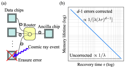
In this work, we take a different approach and use a distributed error correcting scheme to detect and correct correlated errors by CREs. Distributed hardware architectures, connecting smaller nodes into a tightly-coupled system using an interconnect network, have been proposed to achieve scalability for a single computation Duan et al. (2004); Jiang et al. (2007); Kim and Kim (2009); Lim et al. (2006); Nickerson et al. (2013); Oi et al. (2006); Van Meter et al. (2010); Van Meter and Devitt (2016); Monroe et al. (2014). Here, we repurpose these architectures to improve fault tolerance. Our approach is system independent and works as long as a quantum network can be built to share entanglement between separate chips. Since CREs are independent stochastic processes McEwen et al. (2021), there is no correlation between CREs at different chips, when the interconnects are switched off. In a network of chips, a CRE erases information from one chip, but as we show this event and the specific impacted chip can be detected (see Fig. 1a). Since the location of the error is now known, we can use erasure QEC to correct the errors and recover the information Grassl et al. (1997); Knill (2005); Knill et al. (2000); Silva (2004). We present a low-overhead erasure QEC scheme that is fault tolerant against the CREs and discuss its implementation using superconducting chips connected with microwave links (see e.g., Refs. Kurpiers et al. (2018); Axline et al. (2018); Zhong et al. (2021); Gold et al. (2021)), and provide logical-error estimates in state-of-the-art experimental systems. Our analysis indicates that under reasonable assumptions, we are able to suppress the damage from these catastrophic events to higher order and reduce the CRE-induced logical error rate from 1 every 10 seconds in Ref. McEwen et al. (2021) to less than 1 per month. We emphasize that while our estimations of code performance are done for a specific platform, our scheme is general and can be applied to other quantum computing platforms that are severely affected by CREs.
Setup.– We consider two levels of encoding on chips, each containing hundred of qubits. The first level uses an error correcting code (e.g., a surface code Fowler et al. (2012)) to protect the information in each chip. In the second level of encoding, we concatenate this code with a QEC code capable of correcting erasure errors Grassl et al. (1997). The operations in the first level should be protected by the surface code. Therefore, operations in that level are followed by syndrome checks at every step. Upon a CRE on a specific chip, most syndromes of the first-level encoding in that chip will show an error, which reveals the location of the erasure error in the second level. This will subsequently trigger error correction in the second level. We expect that by correcting errors we would be able to suppress the rate of catastrophic events to , where is the CRE rate in a chip and is the time that it takes for the second-level error correction cycle (see Fig. 1b).
For example, we can use the [[4,1,2]] code Grassl et al. (1997) to correct single erasure errors. As shown in Fig. 2b, a single CRE event will trigger the QEC circuit to correct the erasure error and successfully restore the original encoding. However, if there is a second CRE erasure event during the erasure correction, the QEC circuit will fail to restore the encoded information, leading to a CRE-induced logical error rate proportional to , which is already suppressed to the second order in . Note that the QEC for is relatively simple because we only care about correcting single CRE errors and do not worry about CRE errors during the QEC operation. In order to use larger-distance codes, e.g., the code Steane (1996), to suppress the CRE errors to higher orders it is crucial to design the QEC circuit fault tolerantly so that all possible relevant CRE events during the QEC should not damage the encoded information.
Fault tolerant error correction for erasure errors.– We assume that by using sufficiently large surface codes in the first level, Pauli error rates due to the failure of the surface QEC are much lower than the rate of the CREs. As such, we only consider the errors induced by the CREs. For simplicity, we assume that a CRE-induced erasure error could propagate through a two-qubit gate and completely erase both involved qubits 111In practice, the propagation of erasure errors at the surface-code level through the gates depends on both the microscopic detail of the erasures and the implementation of the gates. Here we consider the worst-case scenario, where a single erasure can completely erase all the qubits involved in a multi-qubit gate.. Upon detecting erasure errors on a chip, we replace the erased chip with a chip held in reserve for this purpose. The data qubits on the new chip are randomly initialized. Hence, their erasure errors are converted to detected Pauli errors randomly drawn from after the chip replacement. The weight of an error is assigned by counting the number of qubits on which the error has non-identity support (including the erasure). We propose a novel fault-tolerant QEC (FTQEC) scheme, which we call the erasure-flag scheme, that satisfies the fault-tolerant criteria Aliferis et al. (2006); Gottesman (2010); Chamberland and Beverland (2018) (see also Supplementary Material SM ). The scheme adaptively performs non-destructive stabilizer measurements using one ancilla qubit on an ancilla chip (see Fig. 1a). A single erasure error that occurs on the ancilla could possibly propagate into multiple data erasures on different data chips. We define such errors as bad errors. However, since we can detect such errors immediately, we get extra information about when and where the errors occur. So similar to the flag FTQEC for generic Pauli errors Chao and Reichardt (2018a, b); Chamberland and Beverland (2018), the access to the extra information enables us to design protocols that use minimal resources to tolerate the bad errors. In our context, the extra information comes directly from the first-level QEC and does not require additional resources, e.g. flag qubits, in the second level.

The erasure-flag FTQEC protocol using a distance- code is implemented as follows. (i). Upon detecting erasure errors on the data qubits, replace the erased data qubits (chips), initialize the erasure-flag error set which contains the detected data errors, set which counts the number of bad erasure errors that happen during the protocol and apply the following erasure-QEC. (ii). Measure a set of stabilizers of minimal size that can be used to correct the current . (A). If there are bad erasures detected in the middle of a stabilizer measurement with , stop the measurement immediately, update by adding , replace the erased qubits (chips), update , and restart (ii). (B). Otherwise, apply a correction in based on the measured syndromes.
The fault tolerance of the protocol is guaranteed by the following two key ingredients. (a). Bad erasures can be immediately detected so that we can keep track of the erasure-flag error set resulting from the bad errors. (b). The erasure-flag error set is correctable (different errors either have different syndromes or differ by a stabilizer) if there are fewer than faults. We note that similar to the case of the flag-QEC, the second ingredient cannot always be satisfied, and it depends on the codes and syndrome extraction circuits in general. Here we show that the erasure-flag scheme can be applied to the four-qubit and seven-qubit codes using proper QEC circuits, and in Supplementary Material SM we show that it can be applied, more generally, to other codes including the topological surface codes with arbitrary distance. We show the QEC circuits for the four-qubit and seven-qubit codes in Fig. 2. The FT circuit for the [[4,1,2]] code (Fig. 2b) corrects a single data erasure at the input. A non-FT circuit for the [[7,1,3]] code (Fig. 2c) is triggered by a data erasure error at the input and non-adaptively measures a full set of stabilizers in a fixed sequence. However, an extra erasure that occurs on the ancilla chip during a stabilizer measurement could propagate into multiple data errors and cause a logical failure. As such, the non-FT circuit fails to correct some consecutive double erasures. In contrast, the adaptive FT circuit (Fig. 2d), which keeps track of the possible error set and measures only a minimal set of stabilizers, can tolerate up to two consecutive erasures on arbitrary qubits.

Analysis of the erasure error rates.– Following Ref. McEwen et al. (2021), we model CREs on each chip by a Poisson process , such that , where is the rate of the events whose numerical value is reportedly . Of course, the exact numerical value of depends on the geometry and other specifications of the chip. However, for simplicity, we assume that this rate can be applied to our setup of interest Martinis (2021). Since the events in each chip are independent, the introduction of additional chips increases the overall rate of the events in the system linearly. Using the FT implementation of a QEC code that corrects erasure errors in a cycle, a catastrophic event might occur if there are more than additional events during the recovery time, , following the first event that triggers error correction. Such a catastrophic event leads to a logical failure at the second level of encoding. The rate of these catastrophic events is obtained by taking the product of the rate of the CREs that trigger error correction and the probability that more than CREs happen in time following the first CRE. For a code over chips, the former is . However, since we need an ancilla chip for our QEC scheme, the latter factor should be calculated using the rate . Therefore, we find the rate of the catastrophic events, . For , we can approximate this by , which shows the desired error suppression in this regime. Note that here we considered the worst-case scenario, but not all weight- (or higher) errors are catastrophic, and some are still correctable. Therefore, by considering the longest error correction and recovery time for (see Fig. 2b and d), this analysis gives a lower bound on the memory lifetime, , limited by the coincident CREs within (see solid lines in Fig. 3).
In contrast, for the non-FT implementation of the code, we obtain an upper bound on the memory lifetime (dashed line in Fig. 3). In this case, some double events cause a logical failure. Since we are interested in an upper bound, we only consider the case where the first erasure error occurs on the edge chips in Fig. 2a. Following this event, depending on the affected chip, there are one or two stabilizer measurements during which an ancilla erasure can lead to logical failure. Therefore, for an upper bound, we consider CREs on these 6 edge chips with the rate as triggering events and find the probability of an additional event on an ancilla during one of the stabilizer measurements. Since different stabilizer measurements (colored boxes in Fig. 2c) have the same number of inter-chip gates, we assume that they each take . Therefore, we find the upper bound of for in this case, see Fig. 3.
Since the improvement sensitively depends on the recovery time, , it is crucial to estimate the feasible recovery time for realistic superconducting devices.
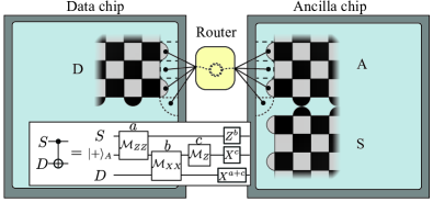
Experimental implementation.– Our proposed scheme can be implemented experimentally in superconducting devices by coupling multiple data chips to an ancilla chip through a router Chang et al. (2020); Zhou et al. (2021) as schematically illustrated in Fig. 1a. The ancilla chip is used to collect the syndrome information by coupling a syndrome patch to the data patches (all encoded in a surface code) associated with different stabilizers. We zoom in on Fig. 1a and show in detail how the ancilla chip is coupled to one of the data chips in Fig. 4. To implement an entangling gate, e.g. , between the syndrome patch S and the data patch D, we introduce an ancilla patch A on the ancilla chip and apply the measurement-based gate Horsman et al. (2012), whose circuit is shown in the inset at the lower-left corner of Fig. 4. The measurement of joint Pauli operators () between the surface patches A and S (D) is implemented by lattice surgery Horsman et al. (2012), i.e. merging and then splitting the () boundaries of the two involved patches. The whole gate using the lattice surgery is fault-tolerant in the surface-code level and compliant with the local constraints in 2D architecture Horsman et al. (2012). The nontrivial part of our setting is that we need to nonlocally merge the boundaries of the A and D patches that sit on different chips. This is done by adding new plaquettes (see the dashed boxes in Fig. 4) that connect the two nonlocal boundaries. For each of the new plaquette, we have two ancilla qubits (see the black dots in Fig. 4), each sitting on one chip and is locally coupled to two data qubits on the boundary of the surface patches. To measure the stabilizer associated with a new plaquette, we first apply a nonlocal gate between the two ancilla qubits to create a Bell state , then apply two gates between the ancilla qubits and their coupled data qubits, apply another nonlocal CX gate between the ancillas and finally measure one of the ancillas. The non-local physical gate between the ancilla qubits can be implemented by teleportation-based gates that use pre-shared and purified bell pairs between two chips as resources Bennett et al. (1996); Wan et al. (2019); Chou et al. (2018); Yan et al. (2022).
We can estimate the length of the outer QEC cycle and the corresponding upper bound of the logical error rate based on realistic experimental parameters in the superconducting architecture. The most time-consuming physical operations are the two-qubit gates (ns Arute et al. (2019); Wu et al. (2021)), measurements (ns Heinsoo et al. (2018)) and inter-chip state transfers (ns Gold et al. (2021); Zhong et al. (2021)). We assume that each surface patch is a rotated surface code and each surface-level operation is followed by a full surface-QEC cycle with 10 rounds of repeated syndrome measurements. For maximum parallelism for all the operations, we estimate that the maximum recovery time for the [[4,1,2]] ([[7,1,3]]) code correcting 1 (2) erasure errors is approximately s (s). See Supplementary Material SM for details. Therefore, based on these estimated recovery times, we obtain a lower bound of the memory lifetimes of approximately 5 hours using the four-qubit, and 51 days for seven-qubit codes, see markers in Fig. 3.
Discussion.– So far we have focused on quantum memory and showed that we can protect the quantum system from catastrophic events for a sufficiently long time using distributed FTQEC. In principle, our scheme can be extended to universal fault-tolerant computing since it is compatible with the existing protocols. Furthermore, the resource overhead required for overcoming the CREs could be less than that required for the standard depolarizing noise. For example, we can prepare the magic states non-fault-tolerantly and verify them by performing erasure detection, without applying costly magic-state distillation Knill (2004); Bravyi and Kitaev (2005), if we only aim to correct the CRE-induced erasure errors.
We can also use Knill-type QEC Knill (2005) to correct erasure errors. The Knill-QEC performs the error correction while teleporting the information from the data block to one of the blocks in a prepared encoded Bell pair. The fault tolerance of the Knill-QEC for general erasure errors is analyzed in Ref. Knill (2005). In Supplementary Material SM , we show the application of the Knill-QEC in our setting. Compared to the erasure-flag scheme, the Knill scheme could be faster since the syndromes are measured in parallel. However, it is more resource-demanding since it requires two extra blocks of qubits encoded as a Bell pair for each logical qubit. Moreover, the preparation of the Bell pair potentially requires a complex coupling structure between the data chips.
Lastly, we discuss the possibility of optimizing the outer QEC to correct both the erasure errors and the Pauli errors uncorrectable by the surface codes. For now, the introduction of the second layer of QEC exponentially suppresses the error rate due to the rare erasure errors while linearly enhancing the error rate due to the Pauli errors resulting from the failure of the surface codes. In the regime where , it is advantageous to consider the tradeoff between and and minimize the total logical error rate by tailoring the outer codes to correct both erasure and Pauli errors. However, the details of the code tailoring, the fault-tolerant QEC design, and the implementation of the universal gates, which might require magic state distillation, remain to be explored.
Acknowledgements.
We thank Vignesh Raman for helpful discussions. We acknowledge support from the ARO (W911NF-18-1-0020, W911NF-18-1-0212), ARO MURI (W911NF-16-1-0349, W911NF-21-1-0325), AFOSR MURI (FA9550-19-1-0399, FA9550-21-1-0209), AFRL (FA8649-21-P-0781), DoE Q-NEXT, NSF (OMA-1936118, EEC-1941583, OMA-2137642), NTT Research, and the Packard Foundation (2020-71479). A.S. is supported by a Chicago Prize Postdoctoral Fellowship in Theoretical Quantum Science. BOS and RV acknowledge the support from JST Moonshot RD Grant (JPMJMS2061).References
- Nielsen and Chuang (2010) M. A. Nielsen and I. L. Chuang, Quantum Computation and Quantum Information: 10th Anniversary Edition (Cambridge University Press, 2010).
- lid (2013) Quantum Error Correction (Cambridge University Press, 2013).
- Clemens et al. (2004) J. P. Clemens, S. Siddiqui, and J. Gea-Banacloche, Phys. Rev. A 69, 062313 (2004).
- Nickerson and Brown (2019) N. H. Nickerson and B. J. Brown, Quantum 3, 131 (2019).
- Alicki et al. (2002) R. Alicki, M. Horodecki, P. Horodecki, and R. Horodecki, Phys. Rev. A 65, 062101 (2002).
- Averin and Fazio (2003) D. V. Averin and R. Fazio, Journal of Experimental and Theoretical Physics Letters 78, 664 (2003).
- Klesse and Frank (2005) R. Klesse and S. Frank, Phys. Rev. Lett. 95, 230503 (2005).
- Aliferis et al. (2006) P. Aliferis, D. Gottesman, and J. Preskill, Quantum Info. Comput. 6, 97–165 (2006).
- Aharonov et al. (2006) D. Aharonov, A. Kitaev, and J. Preskill, Phys. Rev. Lett. 96, 050504 (2006).
- Vepsäläinen et al. (2020) A. P. Vepsäläinen, A. H. Karamlou, J. L. Orrell, A. S. Dogra, B. Loer, F. Vasconcelos, D. K. Kim, A. J. Melville, B. M. Niedzielski, J. L. Yoder, et al., Nature 584, 551 (2020).
- Cardani et al. (2021) L. Cardani, F. Valenti, N. Casali, G. Catelani, T. Charpentier, M. Clemenza, I. Colantoni, A. Cruciani, G. D’Imperio, L. Gironi, et al., Nature communications 12, 2273 (2021).
- McEwen et al. (2021) M. McEwen, L. Faoro, K. Arya, A. Dunsworth, T. Huang, S. Kim, B. Burkett, A. Fowler, F. Arute, J. C. Bardin, et al., Nature Physics 18, 107 (2021).
- Gidney and Ekerå (2021) C. Gidney and M. Ekerå, Quantum 5, 433 (2021).
- Zwanenburg et al. (2013) F. A. Zwanenburg, A. S. Dzurak, A. Morello, M. Y. Simmons, L. C. L. Hollenberg, G. Klimeck, S. Rogge, S. N. Coppersmith, and M. A. Eriksson, Rev. Mod. Phys. 85, 961 (2013).
- Rainis and Loss (2012) D. Rainis and D. Loss, Phys. Rev. B 85, 174533 (2012).
- Martinis (2021) J. M. Martinis, npj Quantum Information 7, 90 (2021).
- Nsanzineza and Plourde (2014) I. Nsanzineza and B. L. T. Plourde, Phys. Rev. Lett. 113, 117002 (2014).
- Patel et al. (2017) U. Patel, I. V. Pechenezhskiy, B. L. T. Plourde, M. G. Vavilov, and R. McDermott, Phys. Rev. B 96, 220501 (2017).
- Henriques et al. (2019) F. Henriques, F. Valenti, T. Charpentier, M. Lagoin, C. Gouriou, M. Martínez, L. Cardani, M. Vignati, L. Grünhaupt, D. Gusenkova, et al., Applied physics letters 115, 212601 (2019).
- Duan et al. (2004) L. M. Duan, B. B. Blinov, D. L. Moehring, and C. Monroe, Quantum Inf. Comput. 4, 165 (2004).
- Jiang et al. (2007) L. Jiang, J. M. Taylor, A. S. Sørensen, and M. D. Lukin, Phys. Rev. A 76, 062323 (2007).
- Kim and Kim (2009) J. Kim and C. Kim, Quantum Information and Computation 9 (2009).
- Lim et al. (2006) Y. L. Lim, S. D. Barrett, A. Beige, P. Kok, and L. C. Kwek, Physical Review A 73, 012304 (2006).
- Nickerson et al. (2013) N. H. Nickerson, Y. Li, and S. C. Benjamin, Nature communications 4, 1756 (2013).
- Oi et al. (2006) D. K. L. Oi, S. J. Devitt, and L. C. L. Hollenberg, Phys. Rev. A 74, 052313 (2006).
- Van Meter et al. (2010) R. Van Meter, T. D. Ladd, A. G. Fowler, and Y. Yamamoto, International Journal of Quantum Information 8, 295 (2010).
- Van Meter and Devitt (2016) R. Van Meter and S. Devitt, IEEE Computer 49, 31 (2016).
- Monroe et al. (2014) C. Monroe, R. Raussendorf, A. Ruthven, K. R. Brown, P. Maunz, L. M. Duan, and J. Kim, Physical Review A 89, 022317 (2014).
- Grassl et al. (1997) M. Grassl, T. Beth, and T. Pellizzari, Phys. Rev. A 56, 33 (1997).
- Knill (2005) E. Knill, Physical Review A 71, 042322 (2005).
- Knill et al. (2000) E. Knill, R. Laflamme, and G. Milburn, arXiv preprint quant-ph/0006120 (2000).
- Silva (2004) M. Silva, arXiv preprint quant-ph/0405112 (2004).
- Kurpiers et al. (2018) P. Kurpiers, P. Magnard, T. Walter, B. Royer, M. Pechal, J. Heinsoo, Y. Salathé, A. Akin, S. Storz, J.-C. Besse, S. Gasparinetti, A. Blais, and A. Wallraff, Nature 558, 264 (2018).
- Axline et al. (2018) C. J. Axline, L. D. Burkhart, W. Pfaff, M. Zhang, K. Chou, P. Campagne-Ibarcq, P. Reinhold, L. Frunzio, S. M. Girvin, L. Jiang, M. H. Devoret, and R. J. Schoelkopf, Nature Physics 14, 705 (2018).
- Zhong et al. (2021) Y. Zhong, H.-S. Chang, A. Bienfait, É. Dumur, M.-H. Chou, C. R. Conner, J. Grebel, R. G. Povey, H. Yan, D. I. Schuster, et al., Nature 590, 571 (2021).
- Gold et al. (2021) A. Gold, J. P. Paquette, A. Stockklauser, M. J. Reagor, M. S. Alam, A. Bestwick, N. Didier, A. Nersisyan, F. Oruc, A. Razavi, B. Scharmann, et al., npj Quantum Information 7, 142 (2021).
- Fowler et al. (2012) A. G. Fowler, M. Mariantoni, J. M. Martinis, and A. N. Cleland, Phys. Rev. A 86, 032324 (2012).
- Steane (1996) A. Steane, Proceedings of the Royal Society of London. Series A: Mathematical, Physical and Engineering Sciences 452, 2551 (1996).
- Note (1) In practice, the propagation of erasure errors at the surface-code level through the gates depends on both the microscopic detail of the erasures and the implementation of the gates. Here we consider the worst-case scenario, where a single erasure can completely erase all the qubits involved in a multi-qubit gate.
- Gottesman (2010) D. Gottesman, in Quantum information science and its contributions to mathematics, Proceedings of Symposia in Applied Mathematics, Vol. 68 (2010) pp. 13–58.
- Chamberland and Beverland (2018) C. Chamberland and M. E. Beverland, Quantum 2, 53 (2018).
- (42) Supplementary Material.
- Chao and Reichardt (2018a) R. Chao and B. W. Reichardt, Physical Review Letters 121, 050502 (2018a).
- Chao and Reichardt (2018b) R. Chao and B. W. Reichardt, npj Quantum Information 4, 42 (2018b).
- Chang et al. (2020) H.-S. Chang, K. J. Satzinger, Y. P. Zhong, A. Bienfait, M.-H. Chou, C. R. Conner, É. Dumur, J. Grebel, G. A. Peairs, R. G. Povey, and A. N. Cleland, Applied Physics Letters 117, 244001 (2020).
- Zhou et al. (2021) C. Zhou, P. Lu, M. Praquin, T.-C. Chien, R. Kaufman, X. Cao, M. Xia, R. Mong, W. Pfaff, D. Pekker, and M. Hatridge, arXiv preprint 2109.06848 (2021).
- Horsman et al. (2012) C. Horsman, A. G. Fowler, S. Devitt, and R. Van Meter, New Journal of Physics 14, 123011 (2012).
- Bennett et al. (1996) C. H. Bennett, G. Brassard, S. Popescu, B. Schumacher, J. A. Smolin, and W. K. Wootters, Physical Review Letters 76, 722 (1996).
- Wan et al. (2019) Y. Wan, D. Kienzler, S. D. Erickson, K. H. Mayer, T. R. Tan, J. J. Wu, H. M. Vasconcelos, S. Glancy, E. Knill, D. J. Wineland, A. C. Wilson, and D. Leibfried, Science 364, 875 (2019).
- Chou et al. (2018) K. S. Chou, J. Z. Blumoff, C. S. Wang, P. C. Reinhold, C. J. Axline, Y. Y. Gao, L. Frunzio, M. Devoret, L. Jiang, and R. Schoelkopf, Nature 561, 368 (2018).
- Yan et al. (2022) H. Yan, Y. Zhong, H.-S. Chang, A. Bienfait, M.-H. Chou, C. R. Conner, E. Dumur, J. Grebel, R. G. Povey, and A. N. Cleland, Phys. Rev. Lett. 128, 080504 (2022).
- Arute et al. (2019) F. Arute, K. Arya, R. Babbush, D. Bacon, J. C. Bardin, R. Barends, R. Biswas, S. Boixo, F. G. S. L. Brandao, D. A. Buell, et al., Nature 574, 505 (2019).
- Wu et al. (2021) Y. Wu, W.-S. Bao, S. Cao, F. Chen, M.-C. Chen, X. Chen, T.-H. Chung, H. Deng, Y. Du, D. Fan, et al., Physical Review Letters 127, 180501 (2021).
- Heinsoo et al. (2018) J. Heinsoo, C. K. Andersen, A. Remm, S. Krinner, T. Walter, Y. Salathé, S. Gasparinetti, J.-C. Besse, A. Potočnik, A. Wallraff, and C. Eichler, Physical Review Applied 10, 034040 (2018).
- Knill (2004) E. Knill, arXiv preprint quant-ph/0402171 (2004).
- Bravyi and Kitaev (2005) S. Bravyi and A. Kitaev, Physical Review A 71, 022316 (2005).