Multiferroic van der Waals heterostructure FeCl2/Sc2CO2:
Nonvolatile electrically switchable electronic and spintronic properties
Abstract
Multiferroic van der Waals (vdW) heterostrucutres offers an exciting route towards novel nanoelectronics and spintronics device technology. Here we investigate the electronic and transport properties of multiferroic vdW heterostructure composed of ferromagnetic FeCl2 monolayer and ferroelectric Sc2CO2 monolayer using first-principles density functional theory and quantum transport simulations. We show that FeCl2/Sc2CO2 heterostructure can be reversibly switched from semiconducting to half-metallic behavior by electrically modulating the ferroelectric polarization states of Sc2CO2. Intriguingly, the half-metallic phase exhibits a Type-III broken gap band alignment, which can be beneficial for tunnelling field-effect transistor application. We perform a quantum transport simulation, based on a proof-of-concept two-terminal nanodevice, to demonstrate all-electric-controlled valving effects uniquely enabled by the nonvolatile ferroelectric switching of the heterostructure. These findings unravels the potential of FeCl2/Sc2CO2 vdW heterostructures as a building block for designing a next generation of ultimately compact information processing, data storage and spintronics devices.
I Introduction
The continuous miniaturization of electronic products posses huge technological challenges on the design of nanoelectronic devices and functional materials. Spintronics and two-dimensional (2D) materials provides new ideas for solving this problem. Compare to the conventional spintronics based on three-dimensional (3D) bulk magnetic materials, 2D-material-based spintronics offers enormous opportunities for the post Moore's law era due to its low energy consumption, fast device operation, mechanical flexibility, high storage density, and gate-controllable operation Soumyanarayanan ; Zhang . The recent advancements of van der Waals (vdW) heterostructure, obtained via the vertical stacking of different 2D materials, further expands the design flexibility and the functionality of 2D-material-based nanoelectronic, optoelectronics and spintronics devices liemao ; li ; liang ; liu ; Gong1 ; zhong ; Novoselov ; ANG_PRB ; ANG_PRB2 ; Cao_APL ; Qing_APL ; Chuong_PRB ; Chuong_NJC ; Chuong_JPCL ; bafekry2020a ; bafekry2020b ; bafekry2020c ; bafekry2020d .
2D materials with intrinsic magnetism are uncommon and often required complex nanofabrication techniques Shi ; Tongay ; jiazhang . Nonetheless, the recent theoretical Guo and experimental Gong ; Huang advancements in 2D materials with intrinsic magnetism have revitalized the exploration of intrinsic magnetism in 2D layered materials for spintronic applicationszhong ; song , such as the very large negative magnetoresistance ratio of over 10,000% in the vdW tunnel junction made of ultrathin magnetic semiconductor CrI3 Kim ; Wang , 100% spin polarization in tunnel junction composed of CrI3 tunnel barrier Paudel , valley splitting and valley-polarized electroluminescence in ultrathin CrI3 vdW heterostructures Zhang1 ; Seyler . Beyond 2D magnetic materials, 2D ferroelectric monolayer has also received intensive research attention in recent years Cui , primarily because of their huge potential in memory and neuromorphic devices Guan as enabled by the presence of electrically-switchable spontaneous ferroelectric polarization. The recent exploration of intrinsic ferroelectric properties in 2D monolayers, such as In2Se3 Ding , 1T-phase MoS2 Shirodkar , MX (M=Ge, Sn; X=S, Se, Te) Fei1 ; Wang2 , bilayer BN Li1 , and CuInP2S2 Qi , have shed much light on the physics and device application potential of 2D ferroelectric materials.
The union of 2D ferroelectric and ferromagnetic materials leads to the emergence of multiferroic vdW heterostructures and devices, in which the all-electric switching of the ferroelectric sub-layer and the magnetic properties of the ferromagnetic sub-layer can be simultaneously combined to render new material properties and device functionalities Gong2 ; Lu ; Sun ; Zhao ; Li2 . Such magnetoelectric effect represents a promising route towards the development of ultracompact and multifunctional nanodevices. The simultaneous presence of two tuning knobs, i.e. the electric fields and the magnetic fields, offers enormous design flexibility in engineering the physical properties of vdW heterostructures for novel electronic, magnetic and spintronic devices with electrically switchable operations.
In this work, we investigate the electronic and the transport properties of a multiferroic vdW heterostructures composed of ferromagnetic FeCl2 monolayer and ferroelectric monolayer Sc2CO2 by using first-principle density function theory (DFT) simulations. Here Sc2CO2 serves as a ferroelectric monolayer with excellent lattice matching with the ferromagnetic FeCl2 monolayer – highly beneficial for the computational design and simulation of heterostructures and devices. We show that the electronic band structures of the FeCl2/Sc2CO2 heterostructure can be flexibly tuned between ferromagnetic and half-metallic phase by changing the ferroelectric polarization of Sc2CO2, and such switching is nonvolatile and reversible. The half-metallic FeCl2/Sc2CO2 heterostructure exhibits a broken-gap Type-III band alignment which can be useful for tunneling-based electronic device applications. Based on nonequilibrium Green's function (NEGF) transport simulation, we design a proof-of-concept two-terminal nanodevice based on the FeCl2/Sc2CO2 heterostructure and concretely demonstrate the presence of valving effects. These findings reveals the potential of multiferroic FeCl2/Sc2CO2 heterostructures as a building block in designing future nanoelectronics and spintronics applications. Although multiferroic heterostructures are receiving increasing research attention recently, the progress of 2D van der Waals heterostructure multiferroic heterostructures are still in very early stages. In particular, there are very few heterostructures that exhibits reversibly switched from semiconducting to half-metallic behavior by electrically modulating the ferroelectric polarization states. As experimental studies and devices fabrications typically prefers to have larger variety of candidate systems, the results presented in this work offer an important new addition to the multiferroic family that can be useful for future studies.
II Computational Methods
The geometrical optimization and the spin-polarized DFT computations are performed using the Vienna ab initio Simulation Package (VASP) Kresse ; Kresse1 , with the generalized gradient approximation (GGA) in the Perdew-Burke-Ernzerhof (PBE) scheme for the exchange-correlation energy functional. The electron-ion interaction is described by the projector augmented wave (PAW) Kresse2 . The kinetic energy cutoff is set to be 500 eV. The first Brillouin zone integration is sampled with the 15 -point meshes. To avoid any artificial interactions between the adjacent slabs, a 20 Å vacuum distance is set along the direction vertical to the contact interface. Based on the D3 method of Grimme for describing the interlayer vdW interaction Grimme , the forces on all atoms less than 0.01 eV/Å are achieved for the structural relaxation. To understand the reliability of DFT-D3 in comparison with other methods, DFT-D2 and vdW-DF are also employed to test the systems studied in this work. Although the interlayer distance varies slightly under different methods, the relative stability of the structures and the calculated band structures are nearly identical to those obtained using DFT-D3 sm , thus confirming the reliability of DFT-D3 method. The energy convergence accuracy is set to 10-6 eV per atom. Dipole corrections are included in all calculations. The results considering the effective Hubbard (with a semiempirical value of eV lixr ) and the spin orbit coupling (SOC) are used for comparison, which are presented in Supplementary Materials sm . Finally, the transport properties for a two-probe device systems are calculated using the Atomistix Toolkit (ATK) 2018 package based on the DFT-LCAO and the NEGF method Soler ; Brandbyge ; Taylor ; Taylor1 . We use the periodic-type, Neumann-type, and Dirichlet-type boundary conditions ChengA in the (orthogonal to the transport direction), (perpendicular to the device plane), (direction of electron transport) directions of the device, respectively. For the -directions, the device is two-dimensionally periodic and infinitely wide. For the -directions, we chose the Neumann boundary condition, which corresponds to a zero electric field at the boundary of the computational box. In the -direction, the boundary condition for the electrostatic potential is determined by the electrostatic potential in the electrodes, corresponding to a Dirichlet boundary condition.
. Stacking (Å) 3.248 3.119 2.725 2.46 2.856 2.677 (Å) 3.248 3.119 3.35 3.13 3.45 3.31 Eb (meV/Å2) -75.1 -82.2 -82.1 -95.5 -80.3 -89.3 Gap (eV) 0.376 0 0.264 0 0.379 0 (eV) 2.062 -0.387 2.072 -0.656 2.004 -0.488 (eV) 5.625 5.21 5.55 5.371 5.613 5.307
III Results and Discussions
III.1 Structural and electronic properties
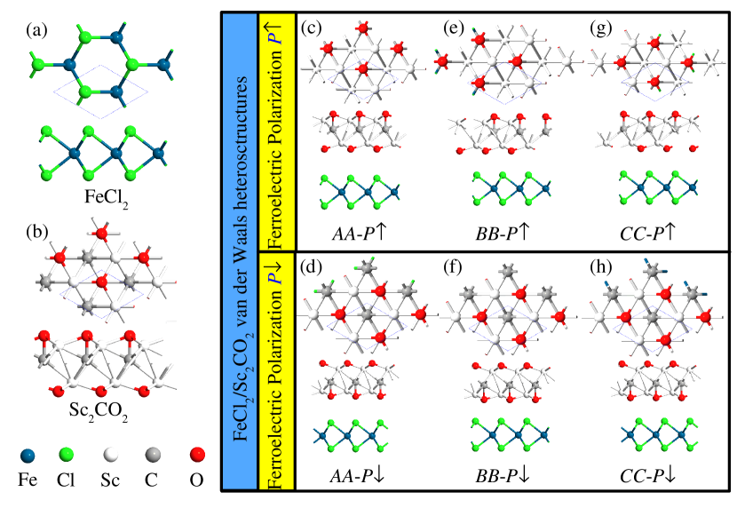
The lattice structures of free-standing ferroelectric monolayer FeCl2 and ferromagnetic monolayer Sc2CO2 are 3.366 Å and 3.41 Å, respectively, which agree with the previously reported values Zhao ; Chandrasekaran ; Zheng [see Figs. 1(a) and 1(b)]. The lattice mismatch is less than 1% when forming the two monolayers stacked vertically to form a 2D/2D vdW multiferroic heterostructure. Although the lattice optimization of both sub-monolayers can be implemented in the calculation of the 2D/2D heterostructure, such relaxation scheme will lead to additional straining effect that modifies the electronic properties of the heterostructures in addition to the weak van der Waals interaction between the 2D sub-monolayer. The lattice vectors of FeCl2 are thus fixed in our calculations to preserve its physical properties and to minimize strain-induced modifications. Three typical stacking configurations, denoted , , and , are considered. Structurally, the three stacking configurations can be described based on the relative location of the O atom: (i) stacking configuration – the O atom in contact with FeCl2 is directly under the Cl atom; (ii) stacking configuration – the O atom at the contact interface is under an empty space of the FeCl2; and (iii) stacking configuration – the O atom is directly under the Fe atom. Since the ferroelectric Sc2CO2 has bistable -polarization states, i.e. and , six different heterostructures were considered [see Figs. 1(c) to 1(h)]. Here, when the carbon atom is closer to the top (bottom) layer, the polarization states becomes (). The detailed structural parameters of the six optimized heterostructures are presented in Table 1. The different stacking configurations produces different optimized interlayer distances when the heterostructures is at equilibrium. The minimum distance between the atoms at the interface (Cl and O atoms) are much larger than the sum of the covalent radii of Cl and O atoms, thus indicating that vdW interactions are the dominant coupling mechanism between the two monolayers.
The binding energy, , of the FeCl2/Sc2CO2 vdW heterostructure is calculated, which is defined as , where is the total energy of FeCl2/Sc2CO2 heterostructure, and represent the energy of the isolated monolayer FeCl2 and Sc2CO2, respectively, and is the surface area at the equilibrium state. The binding energy of the combined systems for all stacking modes are summarized in Table 1. Many studies have shown that the FeCl2 and Sc2CO2 are stable Zheng ; huh ; Chandrasekaran . The calculated binding energies are all negative and are smaller than those of other typical vdW heterostructures Bjorkman ; Padilha , thus confirming that the proposed 2D/2D heterostructures structures simulated in this work are energetically stable and feasible to explore experimentally.
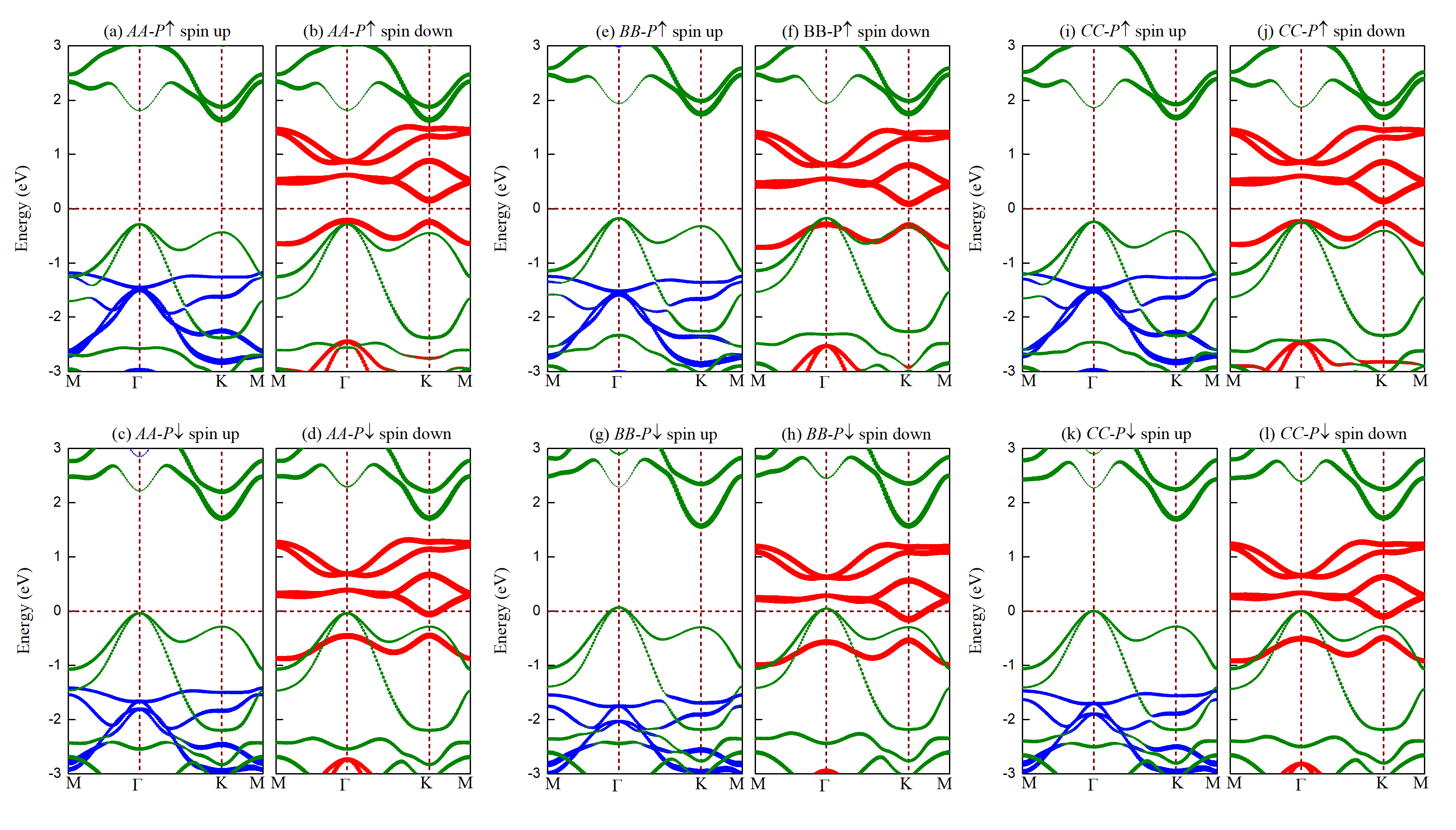
The projected band structures of the multiferroic heterostructures are shown in Fig. 2. Here green, blue and red symbols denote the contributions from Sc2CO2, spin-up and spin-down electronic states of FeCl2, respectively. The band structures of isolated Sc2CO2 and FeCl2 are shown in Fig. S1 of the Supplemental Material sm . In the isolated form, monolayer Sc2CO2 is a semiconductor with a indirect band gap of 1.8 eV Khazaei ; Chandrasekaran , while monolayer FeCl2 is a ferromagnetic semiconductor with the spin-up and spin-down energy gaps of 4.16 and 0.41 eV, respectively. When forming a vdW heterostructures, the electronic band structures of the FeCl2/Sc2CO2 heterostructures exhibit largely a superposition of the electronic states from both materials due to the weak vdW coupling between the two monolayers. The retaining of individual electronic bands structures upon forming a vdW heterostructure is a typical features of 2D/2D vdW heterostructures.
The electronic bands corresponding to the FeCl2 monolayer are sensitively energetically shifted depending on the -polarization states of the Sc2CO2 monolayer. In the case of -polarized Sc2CO2, the electronic states of Sc2CO2 is up-shifted energetically when compared to that of the independent Sc2CO2 monolayer. In this case, a common band gap is retained and the heterostructure behaves as a semiconductor [see Fig. 2, top panel]. In contrast, the electronic properties is more dramatically modified when the -polarization states of the Sc2CO2 monolayer is switched to the -polarization state. In this case, the electronic bands of FeCl2 is energetically down-shifted and crosses the Fermi level, thus transforming the FeCl2 into a half-metal. Furthermore, the spin-down bands of the FeCl2 monolayer (denoted by red symbols in Fig. 2) overlap with the spin-degenerate valence bands (denoted by green symbols in Fig. 2) of the Sc2CO2 monolayer. The heterostructure is thus a half-metallic semimetal with zero common band gap when the ferroelectric polarization of the Sc2CO2 monolayer is switched to the state. Such contrasting electronic properties are particularly evident in the stacking configurations due to its small interlayer distance that strongly couples the two monolayers. In terms of heterostructure band alignment, FeCl2/Sc2CO2 in the half-metallic state exhibits a broken-gap Type-III band alignment under all stacking configurations, (i.e. when material A and material B merge, the resulting heterostructure is type I if the VBM and CBM are contributed by the same monolayer; is type II if the VBM and CBM are contributed by two different monolayers; and is type III if the VBM and CBM are contributed by two different monolayers and overlap with each other. Such band alignment type reveals the potential of FeCl2/Sc2CO2 in tunneling field-effect transistor applications.
We further note that when an Ueff=3 eV is applied to account for a strong correlated effect of the electrons in 3 shell of Fe atoms, the characteristic transformation of the FeCl2 monolayer from the ferromagnetic semiconductor into half-metallic semimetal remains robust (see Fig. S2 of the Supplemental Material sm ). Furthermore, when the SOC is included in the simulations, as shown in Fig. S3 of the Supplemental Material sm , the electronic band structures of the heterostructure exhibit no obvious change with only a slight decrease of the energy band gap. We further note that the observed transformation of the FeCl2 from semiconducting to semimetallic behaviors are also consistent with other 2D/2D multiferroic vdW heterostructures, such as MnCl3/CuInP2S6 Li1 , Cr2Ge2Te6/In2Se3 Gong2 , FeI2/In2Se3 Sun , and CrI3/Sc2CO2 Zhao .
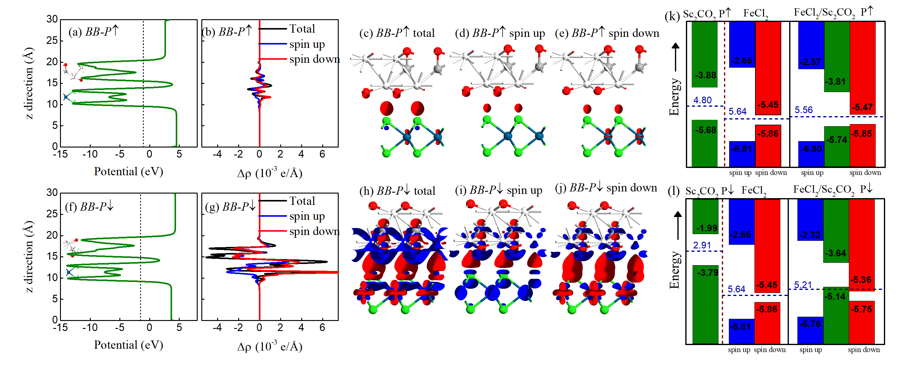
III.2 Mechanism of interfacial interaction and charge redistribution
We attribute the switching behavior discussed above to the electrical interactions mediated by the charge transfer across the FeCl2/Sc2CO2 contact interfaces which is appreciably modified between the and the polarization states. When FeCl2 and Sc2CO2 is constructed into the multiferroic system, the spatial inversion symmetry is broken due to the presence of ferroelectricity, and the charge balance of FeCl2 is perturbed. As a result, the charges redistribute so to allow the system to reach a new equilibrium. The Sc2CO2 monolayer with different polarization states exhibit very different charge transfer characteristics when forming the vdW heterostructure as illustrated in Figs. 3(a) to 3(j). Since the Sc2CO2 is an out-of-plane ferroelectric material, the intrinsic dipole and the in-plane average electrostatic potential differ significantly along the out-of-plane direction for the two -polarization states. When FeCl2 is interfaced with Sc2CO2, the conduction bands of FeCl2 for spin-up and spin-down subbands are all energetically higher than the valence bands of Sc2CO2, while the valence bands of FeCl2 are lower than that of Sc2CO2. Such energy band structures are typical of type-II band alignment [Fig. 3(k)] which hinders the electron transfer between FeCl2 and Sc2CO2. Nonetheless, the built-in electric field with a direction pointing from the Sc2CO2 to the FeCl2 results in a weak electron transfer. Therefore, a small number of electrons accumulates around the FeCl2 as shown in Figs. 3(c) to 3(e). Such interfacial charge transfer process enhances the original internal electric field and leads to a potential step of 2.062 eV across the contact interface. However, such effect is still insufficient to close the common band gap in the FeCl2/Sc2CO2 heterostructure.
In contrast, when the polarity state of Sc2CO2 is switched to , a larger charge transfer changes occurs as the valence band edge of Sc2CO2 becomes energetically higher than the spin-down conduction band of FeCl2 [Fig. 3(l)]. The electrons in the valence bands of Sc2CO2 are sufficiently energetic to transit to the spin-up conduction bands of FeCl2. As shown in the plane-averaged differential charge density and the three-dimensional isosurface of the electron density difference of FeCl2/Sc2CO2 heterostructures in Fig. 3(g) and Figs. 3(h) to 3(j), a large amount of charge transfers occurs from Sc2CO2 to FeCl2. The partial electrons filling of the spin-down subbands of FeCl2 from the Sc2CO2 valence bands causes the conduction bands to shift energetically downwards towards the Fermi level. The overlap between the spin-down conduction band of FeCl2 and the valence band of Sc2CO2 leads to the disappearance of the common gap, and the heterostructure is transformed into a semimetal with Type-III band alignment.
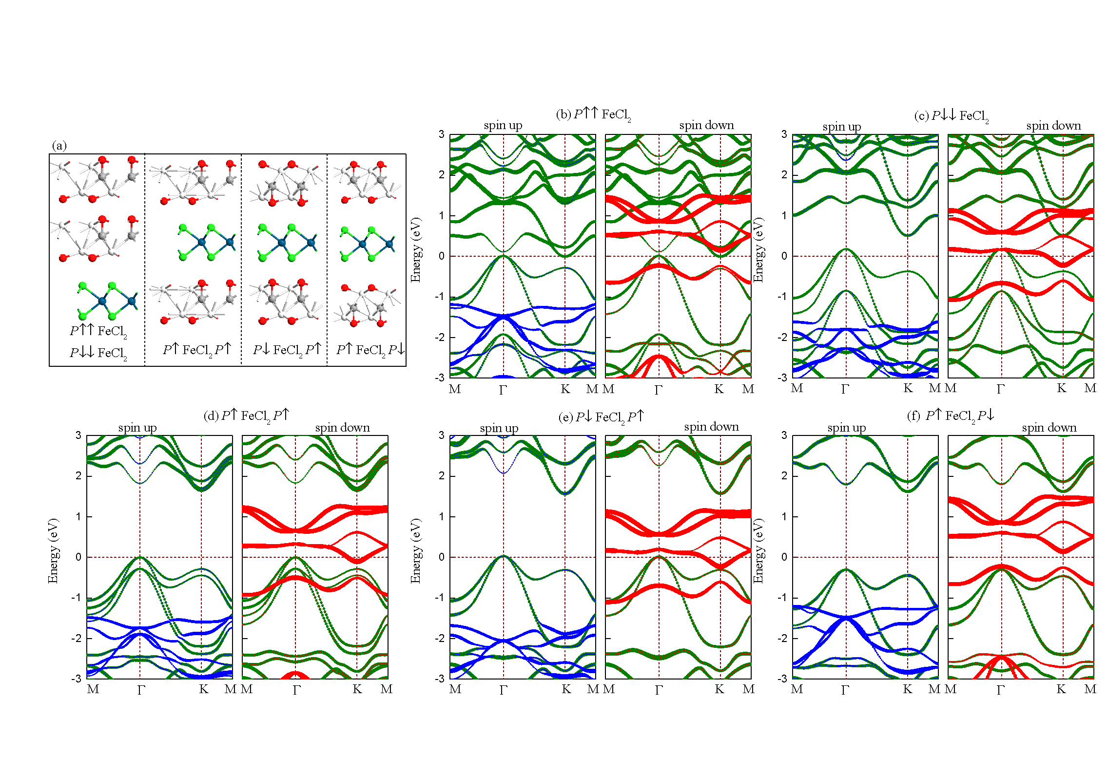
III.3 Structural and electronic properties of the multiferroic heterostructure with the bilayer ferroelectric materials
Studies have shown that increasing the number of polar unit cells can make the free carrier density gradually approach the bound charge density. Therefore, the bilayer Sc2CO2 exhibits metallicity due to the strong covalent interaction between carbon and oxygen sublattices facilitates the development of the necessary potential differenceChandrasekaran , as shown in Supplemental Material sm . The potential difference is twice that of a monolayer, which may cause more charge transfer when it contact with the other materials. The results show that the nature of electronic structure of FeCl2 to be flexibly switched from semiconductor to half-metallic remains by changing the ferroelectric polarization of bilayer Sc2CO2, as shown in Fig. 4(b) and (c). The half-metal phase is more pronounced because of more electron transfer. Three more sandwich configurations were constructed, which the monolayer FeCl2 is -stacked vertically between two monolayer Sc2CO2: FeCl2, FeCl2, and FeCl2, as shown in Fig. 4(a). FeCl2 and FeCl2 are mirror symmetric, which have the same electronic properties. The conduction subband of the spin down of FeCl2 in the polarization state will down-shifted and crosses the Fermi level. This property does not change when add another layer of Sc2CO2 with the same polarity, as can be seen from Fig. 4(d). However, when a layer of Sc2CO2 with opposite polarity is added, the overall polarity disappears. While the internal polarity still exists, and the built-in electric field will redistribute the spatial charge at the interface. Therefore, FeCl2 heterostructure exhibits half-metal properties in the spin down state, and FeCl2 heterostructure is semiconducting, which are similar to monolayer ferroelectric materials.
III.4 Electrically-switchable transport of a two-channel nanodevice: Quantum transport simulation
The two polarization states of and in Sc2CO2 can be reversibly switched by applying an external electric field to the heterostructure, and the polarization state is retained even after the removal of the external electric field. The energy barrier for switching of polarization from the polar to nonpolar configuration is 0.52 eV per formula unit and proceeds via a multistep process of oxygen atom displacements Chandrasekaran . The energy barrier is higher than that of the well-known perovskite ferroelectric LiNbO3(0.26 eV)yem . The switching of the FeCl2/Sc2CO2 vdW heterostructure between the semiconducting and the half-metalic behavior is thus nonvolatile. Importantly, due to the atomic thickness of the FeCl2/Sc2CO2 vdW heterostructure, an external electric field generated by an external gate electrode can readily penetrate across the monolayers, thus allowing such ferroelectric-based polarity switching to be straightforwardly and efficiently achieved all-electrically Fei .
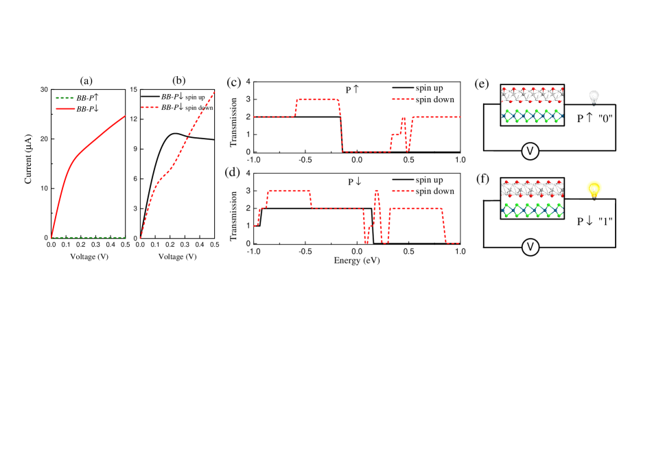
Although memory devices based on multiferroic vdW heterostructures have been previously proposed by Zhao et al Zhao and Li et al Li2 , the transport properties and the nanodevice application capabilities of multiferroic vdW heterostructures remain largely unexplored thus far. Here we construct a two-probe source-channel-drain proof-of-concept device to demonstrate how the vastly contrasting behaviors in and polarization states of the Sc2CO2 monolayer can be harnessed for valving applications. In the Fig. 5(a), we present the simulated curves at room temperature, where the devices exhibit obvious valving effect with a ON-OFF ratio of 3200. Moreover, the magnitude of the current can reach the order of A on the ON state. The spin-up and spin-down currents exhibit different behaviors with the applied bias voltage in the polarization states [see Fig. 5(b)]. The spin-up current decreases when the external bias exceeds 0.23 V, while the spin-down increases monotonously with the external bias. Such contrasting behaviors arises from the spin-dependent band structures of the heterostructures [see Figs. 2(g) and 2(h)]. The spin-up bands have a large band gap above the Fermi level that suppresses electron transport [Fig. 2(g)]. This is in stark contrasts to the case of spin-down bands in which the energy regime around the Fermi level is populated by the spin-down bands contributed by FeCl2 sublayer [Fig. 2(h)]. Such spin-contrasting band structures directly leads to a contrasting spin-up and spin-down currents as observed in Fig. 5(b). We calculate the transmission spectrum of the proposed FeCl2/Sc2CO2 multiferroic vdW heterostructure device at zero bias caolm ; xiacx ; Saraiva ; Zhao3 ; caolie ; qu_NEGF . The Fermi level is set to the zero-energy location. For the P state, a large zero transport gap exists around the Fermi level for both spin-up and spin-down channel, which essentially switches off the electrical current in the device [Figs. 5(c) and 5(e)], thus providing a valving effect. Such transport gap arises directly from the semiconducting nature of the the FeCl2/Sc2CO2 heterostructure when the Sc2CO2 monolayer is electrically switched to -polarization. On the other hand, when the Sc2CO2 monolayer is electrically switched to the -polarization, the heterostructure becomes semimetallic which opens up the transport channel with a large transmission coefficient around the Fermi level, thus allowing an electrical current to flow in the device [Figs. 5(d) and 5(f)].
IV Conclusions
In summary, we investigated the electronic properties of the FeCl2/Sc2CO2 multiferroic van der Waals heterostructure by using first-principles density functional theory and nonequilirbrium Green's function transport simulations. We show that the electronic properties of the FeCl2/Sc2CO2 heterostructures can be reversibly controlled by electrically switching the ferroelectric polarization state of the Sc2co2 monolayer, thus enabling a great wealth of novel functionalities to be derived from FeCl2/Sc2CO2. The half-metallic state of FeCl2/Sc2CO2 exhibits Type-III band alignment, thus suggesting a potential in tunneling field-effect transistor applications. The quantum transport simulation of a proof-of-concept two-terminal device demonstrated the capability of FeCl2/Sc2CO2 heterostructure for valving applications. These findings reveal the potential of FeCl2/Sc2CO2 heterostructure as a building block for designing a next generation of ultracompact and all-electric-controlled spintronics nanodevices.
Acknowledgements
L.C. is supported by the National Natural Science Foundation of China (Grant No. 12104136) and by Scientific Research Fund of Hunan Provincial Education Department(Grant No. 21B0622). G. Z. acknowledges the support of National Natural Science Foundation of China (Grant No. 12174100). Y.S.A. acknowledges the support of SUTD Startup Research Grant (Project No. SRT3CI21163). L.K.A. acknowledges the support of Singapore Ministry of Education Academic Research Fund (MOE AcRF) Tier 2 grant (2018-T2-1-007) and A*STAR AME IRG grant (RGAST2007). All the calculations were carried out using the computational resources provided by the National Supercomputing Centre (NSCC) Singapore.
References
- (1) A. Soumyanarayanan, N. Reyren, A. Fert, C. Panagopoulos, Nature 539, 509 (2006).
- (2) W. Zhang, P. K. J. Wong, R. Zhu, and A. T. S. Wee, InfoMat 1, 479 (2019).
- (3) L. M. Cao, G. H. Zhou, Q. Y. Wu, S. Y. Yang, H. Y. Yang, Y. S. Ang, and L. K. Ang, Phys. Rev. Appl. 13, 054030 (2020).
- (4) H. Li, S. Ruan, and Y. J. Zeng, Adv. Mater. 31, 1900065 (2019).
- (5) S. J. Liang, B. Cheng, X. Cui, and F. Miao, Adv. Mater. 32, 1903800 (2019).
- (6) Y. Liu, Y. Huang, and X. F. Duan, Nature 567, 323 (2019).
- (7) C. Gong and X. Zhang, Two-dimensional magnetic crystals and emergent heterostructure devices, Science, 363, 706 (2019).
- (8) D. Zhong, K. L. Seyler, X. Linpeng, R. Cheng, N. Sivadas, B. Huang, E. Schmidgall, T. Taniguchi, K. Watanabe, M. A. McGuire, W. Yao, D. Xiao, K. M. C. Fu, and X. Xu, Sci. Adv., 3 e1603113 (2017).
- (9) K. S. Novoselov, A. Mishchenko, A. Carvalho, and A. H. Castro Neto, 2D materials and van der Waals heterostructures, Science 353, 6298 (2016).
- (10) Y. S. Ang, L. K. Ang, C. Zhang, and Z. Ma, Phys. Rev. B 93, 041422 (2016).
- (11) Y. S. Ang, S. A. Yang, C. Zhang, Z. Ma, and L. K. Ang, Phys. Rev. B 96, 245410 (2017).
- (12) L. Cao, G. Zhou, Q. Wang, L. K. Ang, and Y. S. Ang, Appl. Phys. Lett. 118, 013106 (2021).
- (13) Q. Wu, L. Cao, Y. S. Ang, and L. K. Ang, Appl. Phys. Lett. 118, 113102 (2021).
- (14) C. V. Nguyen, Phys. Rev. B 103, 115429 (2020).
- (15) K. D. Pham, L. V. Tan, M. Idrees, B. Amin, N. N. Hieu, H. V. Phuc, L. T. Hoa, N. V. Chuong, New J. Chem. 44, 14964-14969 (2020).
- (16) C. Nguyen, N. V. Hoang, H. V. Phuc, Y. S. Ang, C. V. Nguyen, J. Phys. Chem. Lett. 12, 5076-5084 (2021).
- (17) A. Bafekry, M. M. Obeid, C. V. Nguyen, M. Ghergherehchi and M. Bagheri Tagani, J. Mater. Chem. A 8, 13248 (2020).
- (18) A. Bafekry, C. Stampfl and M. Ghergherehchi, Nanotechnol. 31, 295202 (2020).
- (19) A. Bafekry, M. Faraji, A. Abdollahzadeh Ziabari, M. M. Fadlallah, C. V. Nguyen, M. Ghergherehchi and S. A. H. Feghhi, New J. Chem. 45, 8291 (2021).
- (20) A. Bafekry and M. Neek-Amal, Phys. Rev. B 101, 085417 (2020).
- (21) H. Shi, H. Pan, Y. W. Zhang, and B. I. Yakobson, Phys. Rev. B 88, 205305 (2013).
- (22) S. Tongay, S. S. Varnoosfaderani, B. R. Appleton, J. Wu, and A. F. Hebard, Appl. Phys. Lett. 101, 123105 (2012).
- (23) J. Zhang, J. M. Song, K. P. Loh, J. Yin, J. Ding, M. B. Sullivian, and P. Wu, Nano Lett. 7, 2370 (2007).
- (24) Y. Guo, B. Wang, X. Zhang, S. Yuan, L. Ma, and J. Wang, InfoMat 2, 639-655 (2020).
- (25) C. Gong, L. Li, Z. Li, H. Ji, A. Stern, Y. Xia, T. Cao, W. Bao, C. Wang, Y. Wang, Z. Qiu, R. Cava, S. G. Louie, J. Xia, and X. Zhang, Nature 546, 265 (2017).
- (26) B. Huang, G. Clark, E. Navarro-Moratalla, D. R. Klein, R. Cheng, K. L. Seyler, D. Zhong, E. Schmidgall, M. A. McGuire, D. H. Cobden, W. Yao, D. Xiao, P. Jarillo-Herrero, and X. Xu, Nature 546, 270 (2017).
- (27) T. Song, X. Cai, M. W.-Y. Tu, X. Zhang, B. Huang, N. P. Wilson, K. L. Seyler, L. Zhu, T. Taniguchi, K. Watanabe, M. A. McGuire, D. H. Cobden, D. Xiao, W. Yao, and X. Xu, Science 360, 1214 (2018).
- (28) Z. Wang, L. Gutiérrez-Lezama, N, Ubrig, M. Kroner, M. Gibertini, T. Taniguchi, K. Watamane, A. Imamoǧlu, E. Giannini, and A. F. Morpurgo, Nat. Commun. 9, 2516 (2018).
- (29) H. H. Kim, B. Yang, T. Patel, F. Sfigakis, C. Li, S. Tian, H. Lei, and A. W. Tsen, Nano Lett. 18, 4885 (2018).
- (30) T. R. Paude, and E. Y. Tsymbal, ACS Appl. Mater. Interfaces 11, 15781 (2019).
- (31) K. L. Seyler, D. Zhong, B. Huang, X. Linpeng, N. P. Wilson, T. Taniguchi, K. Watanabe, W. Yao, D. Xiao, M. A. McGuire, K. M. C. Fu, and X. Xu, Nano Lett. 18, 3823 (2018).
- (32) Z. Zhang, X. Ni, H. Huang, L. Hu, and F. Liu, Phys. Rev. B 99, 115441 (2019).
- (33) C. Cui, F. Xue, W.-J. Hu, and L.-J. Lain, NPJ 2D Mater. Applications 2, 18 (2018).
- (34) Z. Guan, H. Hu, X. Shen, P. Xiang, N. Zhong, J. Chu, and C. Duan, Adv. Electron. Mater. 6, 1900818 (2020).
- (35) W. Ding, J. Zhu, Z. Wang, Y. Gao, D. Xiao, Y. Gu, Z. Zhang, and W. Zhu, Nat. Commun. 8, 14956 (2017).
- (36) S. N. Shirodkar, and U. V. Waghmare, Phys. Rev. Lett. 112, 157601 (2014).
- (37) R. Fei, W. Kang, and L. Yang, Phys. Rev. Lett. 117, 097601 (2016).
- (38) H. Wang, and X. Qian, Nano Lett. 17, 5027 (2017).
- (39) L. Li, and M. Wu, ACS Nano 11, 6382 (2017).
- (40) J. Qi, H. Wang, X. Chen, and X. Qian, Appl. Phys. Lett. 113, 043102 (2018).
- (41) C. Gong, E. M. Kim, Y. Wang, G. Lee, and X. Zhang, Nat. Commun. 10, 2657 (2019).
- (42) Y. Lu, R. Fei, X. Lu, L. Zhu, L. Wang, and L. Yang, ACS Appl. Mater. Interfaces 12, 6243 (2020).
- (43) W. Sun, W. Wang, D. Chen, Z. Cheng, and Y. Wang, Nanoscale 11, 9931 (2019).
- (44) Y. Zhao, J.-J. Zhang, S. Yuan, and Z. Chen, Adv. Funct. Mater. 29, 1901420 (2019).
- (45) Z. Li, and B. Zhou, J. Mater. Chem. C 8 , 4534-4541 (2020).
- (46) G. Kresse and J. Furthmüller, Phys. Rev. B 54, 11169 (1996).
- (47) G. Kresse and J. Furthmüller, Comput. Mater. Sci. 6, 15 (1996).
- (48) G. Kresse and D. Joubert, Phys. Rev. B 59, 1758 (1999).
- (49) S. Grimme, J. Antony, S. Ehrlich and H. Krieg, J. Chem. Phys. 132, 154104 (2010).
- (50) See Supplemental Material at XXXXX for more details on the band structures of isolated monolayers, projected band structures of the heterostructures with SOC, LDA+ ( eV) and different vdW correction methods.
- (51) X. Li, Z. Zhang and H. Zhang, Nanoscale Adv 2, 495-501 (2020).
- (52) J. M. Soler, E. Artacho, J. D. Gale, A. García, J. Junquera, P. Ordejón, and D. Sáchez-Portal, J. Phys. Condens. Matter 14, 2745 (2002).
- (53) M. Brandbyge, J. L. Mozos, P. Ordejón, J. Taylor, and K. Stokbro, Phys. Rev. B 65, 165401 (2002).
- (54) J. Taylor, H. Guo, and J. Wang, Phys. Rev. B 63, 245407 (2001).
- (55) J. Taylor, H. Guo, and J. Wang, Phys. Rev. B 63, 121104 (2001).
- (56) A. H. D. Cheng, D. T. Cheng, Eng. Anal. Bound. Elem. 29, 268 (2005).
- (57) A. Chandrasekaran, A. Mishra, and A. K. Singh, Nano Lett. 17, 5, 3290 (2017).
- (58) H. Zheng, H. Han, J. Zheng, and Y. Yan, Solid State Commun. 271, 66 (2018).
- (59) H. Hu, W.-Y. Tong, Y.-H. Shen, X. Wang, C.-G. Duan, npj Comput. Mater. 6, 129 (2020).
- (60) T. Björkman, A. V. Krasheninnikov and R. M. Nieminen, Phys. Rev. Lett. 108, 235502 (2012).
- (61) J. F. Padilha, A. Fazzio, and Antônio J. R. da Silva, Phys. Rev. Lett. 114, 066803 (2015).
- (62) M. Khazaei, M. Arai, T. Sasaki, C.-Y. Chung, N. S. Venkataramanan, M. Estili, Y. Sakka, Y. Kawazoe, Adv. Funct. Mater. 23, 2185 (2013).
- (63) M. Ye, D. Vanderbilt, Phys. Rev. B: Condens. Matter Mater. Phys. 93, 134303 (2016).
- (64) Z. Fei, W. Zhao, T. A. Palomaki, B. Sun, M. K. Miller, Z. Zhao, J. Yan, X. Xu, and D. H. Cobden, Nature 560, 336 (2018).
- (65) C. Xia, J. Du, M. Li, X. Li, X. Zhao, T. Wang, and J. Li, Phys. Rev. Appl. 10, 054064 (2018).
- (66) L. M. Cao, X. B. Li, M. Zuo, C. X. Jia, W. H. Liao, M. Q. Long, and G. H. Zhou, J. Magn. Magn. Mater. 485, 136 (2019).
- (67) H. Qu, W. Zhou, S. Guo, Z. Li, Y. Wang, and S. Zhang, Adv. Electron. Mater. 5, 1900813 (2019).
- (68) A. Saraiva-Souza, M. Smeu, J. G. da Silva Filho, E. C. Girão, and H. Guo, J. Mater. Chem. C 5, 11856 (2017)).
- (69) C. C. Zhao, S. H. Tan, Y. H. Zhou, R. J. Wang, X. J. Wang and K. Q. Chen, Carbon 113, 170 (2017).
- (70) L. Cao, Y. S. Ang, Q. Wu, and L. K. Ang, Phys. Rev. B 101, 035422 (2020).