Room temperature deep UV photoluminescence from low dimensional hexagonal boron nitride prepared using a facile synthesis
Abstract
Evaluation of the defect levels in low-dimensional materials is an important aspect of quantum science. In this article, we report a facile synthesis method of hexagonal boron nitride (h-BN) and evaluate the defects and their light emission characteristics. The thermal annealing procedure is optimized to obtain clean h-BN. The UV-Vis spectroscopy shows the optical energy gap of 5.28 eV which is comparable to the reported energy gap for exfoliated, clean h-BN samples. The optimized synthesis route of h-BN has generated two kinds of defects which are characterised using room temperature photoluminescence measurements. The defects emit light at 4.18 eV (in deep ultraviolet region) and 3.44 eV (ultraviolet), respectively. The defect emitting deep ultraviolet (DUV) has oscillatory dependency on the excitation energy, while that emitting 3.44 eV light (ZPL3.44 eV) has a phonon bands with mean energy level separation of 125 meV measured at room temperature. This agrees very well with the Franck-Condon-like structure having regularly spaced energy levels, which are typical indications of single defect levels in the low dimensional h-BN.
keywords:
Photoluminescence, defects, hBN,+91 9742430830 \abbreviationsPL, XRD, UV
1 Introduction
Ever since graphene is exfoliated from graphite, curiosity in low dimensional materials has been exponential and efforts in understanding the physics in low dimensions has regained importance1, 2, 3. Various low dimensional materials have been studied which are stable at room temperature4, 5. These materials show thickness dependent physical properties such as electronic band structure and energy gap as in the case of MoS2 and show quantum size effects. Graphene as such lacks electronic energy gap, which is required for suitability in the electronic industry. MoS2 is another two-dimensional material studied extensively in the last two decades, which has an intrinsic electronic energy gap down to monolayer. Single layer of MoS2 shows direct energy gap of 1.8 eV and indirect energy gap of 2 eV 4, 6, 7. The electronic properties are completely different for a monolayer and multilayered materials. Since materials like MoS2 can be exfoliated easily, much of the effort has been to use them in fabrication of nanoelectronic devices. Tremendous research has been done to use such monolayers to fabricate hetero structures with various other low dimensional materials and thin films8, 9. From a no-gap graphene to moderate energy gap materials such as MoS2 and chalcogenides have been studied for a decade now10, 11, 12, 13. It is a well-established fact that majority of these low dimensional materials show a change in the electronic band structure with number of layers resulting in direct-indirect band gap transition. Materials like monolayer MoS2 and InSe show direct band gap around 1.8 eV, while the energy gap reduces to bulk value of about 1.2 - 1.25 eV when measured for 2-4 monolayers 6, 14.
Recently, the two-dimensional wide band gap materials have also attracted lot of attention. Materials such as hexagonal boron nitride (h-BN), Silicon Carbide (SiC) and diamond(C) has attracted much attention due to their extremely large electronic energy gap at monolayer limit ( 6eV) and also stability at room temperature15, 16, 17, 18, 19, 20, 21. In particular, the hexagonal boron nitride (h-BN) shows layered structure similar to graphene. In view of this, h-BN can be considered as a versatile material for electronic devices. h-BN shows hexagonal lattice with an alternative boron-nitrogen arrangement within the lattice, which is quite similar to the atomic arrangement of graphene. It is quite fascinating that even though h-BN and graphene(C) show similar atomic arrangements (the nearest neighbour distance, lattice parameters and interlayer spacing), h-BN shows a large energy gap (6 eV), while ’pure’ graphene has no energy gap22. Majority of the studies performed on h-BN is by using bulk single crystal and mechanically exfoliating single to few layers of h-BN. Despite the extensive research performed on this material, the fundamental question about the energy gap remains still debatable23, 24. The ab-initio calculations and photoluminescence experiments give quite contrasting interpretations with large scatter in the values for the energy gap (Eg). While the ab-initio calculations predicting an indirect band gap, the optical measurements indicate a direct band gap25, 26, 27, 28, 29. The electronic band structure undergoes a crossover from indirect band gap (bulk h-BN) to direct band gap (monolayer h-BN)30. In this context, h-BN is a wide band gap layered material which hosts extremely bright light emitting defect centres stable at room temperature 31, 32. The defects present in these two dimensional materials emitting single photon has been studied recently. This is a primary requirement for single photon emitting source and quantum photonics 31, 33, 34, 35. Theoretical investigations on monolayer hexagonal boron nitride reveals overestimated wide energy gap compared to experimentally observed value. The energy gap calculated using the density functional theory (DFT) calculations by the Bethe-Salpeter equation is more than 7 eV36, 37. On the other hand, there are reports about calculations giving 6.47 eV using DFT-VASP, yet there is no agreement between various procedures adopted in the calculations. Recently, experiments performed on h-BN/Graphite using scanning tunneling microscopy/spectroscopy (STM/STS) suggested an energy gap of 6.8 0.2 eV 38. The optical energy gap calculations of monolayer h-BN are determined by the exciton energy and a range of energy gap values from 5.30 – 6.30eV have been calculated 36. h-BN is also successfully synthesized using a variety of other techniques such as atomic layer deposition39, chemical vapour deposition40 ,molecular beam epitaxy 41, 30 and layer-by-layer sputtering process42. The low dimensional wide band gap materials not only find their importance in the nanoscale transistor design, but also for hosting the fundamental unit of quantum information processing i.e. qubit43. In this case, a two level quantum system is idealised and a transition between these two energy levels will emit a photon of a given wavelength. An ideal two level system is provided by an isolated defect in 2-dimensional material having large energy gap. Two-dimensional (2-D) systems which are structurally open, demonstrating the quantum confinement, and then reduced charge screening are ideal qualities for hosting the single photon emitters (SPE’s). Since the electronic states of the single defect is well separated by the energy bands of the host lattice, it can be controlled by using the polarized light44, 45. For example, the colour centres in nano-diamonds are one such material platform which are stable and give good emission46. Similarly, the h-BN nanoparticles can host desirable defect centres which could be used in devices for quantum technologies. Interestingly, even a medium energy gap 2-dimensional material such as MoS2 is also capable of hosting isolated defects. In a recently published article, it has been proved that sulphur defects can be prepared controllably using He-ion radiation which act as single photon emitter47. In essence, these defects are excellent candidates for quantum emission. The advancement in the techniques used in miniaturisation of electronic devices has led to conceive these atomic scale devices using either atoms or molecules.
The possible use of h-BN in the graphene based transistor design is very promising. Firstly, there is a good lattice match resulting in a low strained heterostructures and h-BN showing large band gap is essential as a dielectric in the transistor design. There have been numerous reports on the mechanism of dielectric breakdown of a few layer h-BN using local breakdown studies. Notably, the nanoscale measurements using atomic force microscopy/spectroscopy are very crucial for understanding the fundamental mechanism of dielectric breakdown48.
We adopted a simple facile procedure to synthesize multilayered h-BN. Herein, we report the fundamental analysis of prepared h-BN multilayers using X-ray diffraction, UV-Vis spectroscopy, and X-ray photoelectron spectroscopy (XPS). Further, detailed photoluminescence studies been performed at room temperature to understand the defect energy levels and their light emitting properties.
2 Results and discussion
2.1 Experimental Details
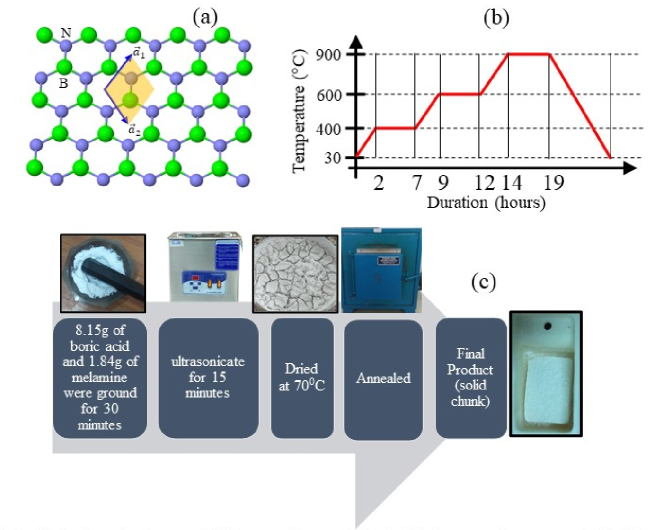
In a typical synthesis procedure as shown in Fig (1), 8.15g of boric acid and 1.84g of melamine (in total 10g of the initial precursors by weight) are taken and mixed well using mortar and pestle for 30 min and then transferred to a beaker containing methanol. This precursor mixture was ultrasonicated for two hours and then dried at 70∘C, refer Fig. (1c). Once the material is completely dried, it is transferred to a Alumina boat and placed in a furnace in an ambient condition. We have tested various heating cycles considering the evolution of nitrogen from the melamine source, desorption of oxygen from the materials at different temperature. The heating cycle which resulted in pure hexagonal boron nitride is shown in fig.(1b). The sample is heated with a heating rate of 6∘C/min to 400∘C and kept it for 5 hours. Here, the melamine molecules partially dissociate into a nitrogen rich precursor for the h-BN. In the second stage, the temperature is raised to 600∘C and kept for 3 hours. In this step, the boric acid partially dissociate to give rise to a boron rich precursor for h-BN. In the third stage, the temperature is taken to 900∘C and kept for 5 hours. At this temperature, boron- and nitrogen-rich precursors will react to give the boron nitride. Here the material is kept for sufficient duration to complete the reaction and then allowed to cool down naturally to room temperature. The appearance of the h-BN immediately taken out of the furnace is shown in the fig.(1e) appears as a white solid chunk. The actual reaction mechanism is shown in fig.S1(sup. information)
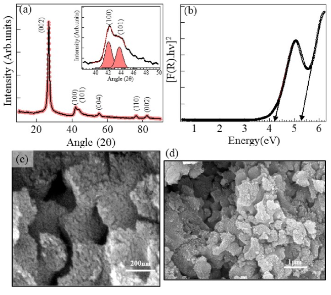
The phase purity and crystalline structure of the synthesized material is examined using X-ray diffraction(XRD). We use CuK1 radiation with wavelength of 1.504Å and the data was collected from 10 - 90∘(2) with a scanning rage of 2∘/min. Fig.(2) shows the XRD pattern obtained for the sample prepared with optimized annealing conditions. The principle diffraction peak is located at 2 26.9∘ which is assigned for the (002) peaks of the h-BN49, 50. This peak pattern indicates that there is a similarity between graphite like h-BN structure.
Further, much weaker peaks are observed at 42∘ and 43.7∘ from the (100)/(101) in close agreement with the reported values in the literature. The broad peaks at this position represents stacking faults in the (100) planes51. Such broad peaks are attributed to the ‘turbostatic’ structure mentioned in the literature. However, the XRD peaks at this diffraction angle can be clearly resolved which is close to the hexagonal boron nitride as shown in the inset Fig.(2a). Further, the peaks [55.25∘, (004)], [76.3∘, (110)] and [76.3∘, (002)] are indicative of a clearly formed single crystalline h-BN. The interlayer spacing of the (002) crystallographic planes is calculated using Bragg’s law and we obtain a value of 0.331 nm which is very close to the ideal value of 0.333 nm for hexagonal boron nitride. Corroborating our XRD analysis, the high resolution electron microscopy images confirm large area layers of h-BN in the form of multilayers. As shown in Fig.(2c and d), large area h-BN layers are formed. At this point, we are not able to separate them as single sheets. Efforts are underway to separate these sheets resulting into single sheets.
Next step is to determine the optical band gap and we used the standard UV-vis spectrometer to determine the absorbance, reflectance of the light by dried h-BN sample. The sample was ultrasonicated for prolonged duration before drying. We use the absorbance to calculate the optical energy gap by means of Tauc plot. As can be seen in fig.(2b), the calculated energy gap is about 5.28 eV which agrees very well with the reported energy gap values52. It is to be noted that there is a large scatter in the determination of the optical band gap of h-BN in the literature. The energy gap measured in our samples match very well with the values obtained using UV-vis spectrum available in the literature52. Additionally, we also can see a strong band of energy lying about 4.2 eV from the valence band edge. This is attributed to the defects which are discussed in detail in the later sections.
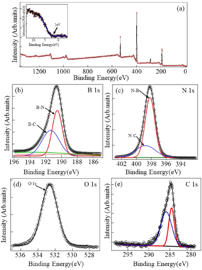
To find out the chemical nature of the individual elements in h-BN multilayers, survey scan and the narrow energy XPS scans are performed around the binding energies of boron (B), nitrogen(N), carbon(C) and oxygen (O). Global spectra of h-BN is shown in the Fig.(3a) demonstrates a typical spectrum with narrow peaks at various binding energy values characteristic of high quality sample. The survey scan depicts binding energy peaks at 190.56 eV, 284.59 eV, 398.15 eV and 532.64 eV correspond to B(1s),C(1s),N(1s) and O(1s) from the h-BN sample respectively. Firstly, the valence band maximum (VBM) can be calculated by performing a high-resolution scan near the Fermi energy. As shown in the inset of Fig.(3a), the VBM was calculated by considering the intersection of the flat XPS energy approaching the valence band(VB) of h-BN and the linear fit of the valence band edge in the XPS data. Such a calculation give us the VBM at 2.0 eV below the Fermi energy. This is in very good agreement with the angle resolved photoemission spectroscopy (ARPES) measurement on h-BN/(graphite), h-BN/Ir(111)and h-BN single crystal where the VBM has been found at 2.2 - 2.8 eV below the Fermi energy. This implies that our facile synthesis method has resulted in a very good quality hexagonal boron nitride. We take the binding energy of carbon (C 1s) at 284.59 eV as shown in the inset of Fig.(3b) as reference in all our analysis. The main peak is at 284.59 eV arising from the sp2 hybridization of carbon coming from the carbon support. The small shoulder peak arising at 285.56 eV can be attributed to C-O bond which could be from the adsorbed oxygen on the surface of h-BN53. The most dominant peak for boron is 190.56 eV which is very close to the ideal value of boron position in hexagonal boron nitride 54. This peak corresponds to the B-N bond in h-BN. The maximum intensity of B-N peak at 190.56eV shows the formation of hexagonal phase of boron nitride54, 55, 56. A small shoulder can be seen in higher energy at 191.56eV representing the B-C bond. Even though the survey scan does show a strong oxygen peak, it is not bonded to the boron atom giving a B-O binding energy at 192 eV 57. From this it is clear that the oxygen peak shown in the full scan arises from the residual gas which is adsorbed on the surface58. As reported in the results from various groups, the enhanced peak at 532.8eV attributed to the boron – oxygen bonding (corresponding to B2O3) is not seen in our sample, thereby reconfirming a complete hexagonal boron nitride phase formation in our sample. The high resolution binding energy scan of nitrogen (N 1s)occurs at 398.15 eV correspond to the N-B bonding and a small shoulder exists at 399.2eV which can be attributed to N-C bond. Interestingly, the binding energy scan of oxygen shows up at 532.67 eV which is due to the presence of B-O bond. We assign this peak to the bond formation during the ultrasonication of the h-BN layers. This can indicate the presence of numerous functional groups on the h-BN surface.
Careful analysis of the XPS spectrum and the BE position of various peaks reveal rich information about the defects present in h-BN. To support this, photoluminescence measurements has been a usual method employed to identify atomic scale defects in h-BN16. Recently, using the Density functional theory (DFT), ab-initio calculations and core level binding energy calculations, the deconvoluted broad XPS spectrum positions were used to assign certain kind of defects in the h-BN lattice 59, 60. Further, there are variety of defects observed in h-BN such as a neutral nitrogen vacancy (VN), single electron trapped nitrogen vacancy (VN)-1, a carbon atom replacing nitrogen (CN) and some complex defects such as NBVN 61, 62, 63. Most of the time, a nitrogen vacancy is either neutral or single occupied (VN) are predominant in h-BN samples which can be categorised as process induced defect is seen.
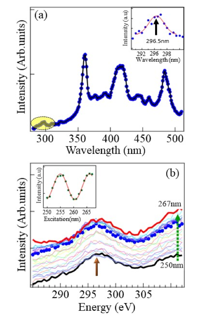
In order to check if our synthesis procedure resulted in such defects and decipher their light emitting properties, room temperature photoluminescence (PL) spectra was taken. As usual, the h-BN multilayered sample was excited using deep-UV light and check the emission lines. Since our sample contains multilayered h-BN, we expected luminescence from various defect levels present in the sample. In particular, when excited with 265nm(4.7 eV) photons and we achieved well resolved photoluminescence spectral. The selection of excitation wavelength(energy) is based on our Tauc plot where we have seen an additional band edge at 4.2 eV (see Fig.2b). A typical photoluminescence spectra is shown in Fig.(4a). A series of emission lines varying in energy position can be seen. Since our first interest is to understand the additional band edge observed in Tauc plot, the scan range in PL is restricted to small wavelength range up to 510 nm. Firstly we will discuss the PL spectra at lower wavelength (DUV) as shown in Fig(4a) (highlighted in yellow). For clarity, this is plotted in the inset of Fig.(4a). The Gaussian fit of the data in this wavelength range shows the peak position at 296.5 nm (4.18 eV). This PL intensity is often attributed to the presence of carbon substituted Nitrogen (VN) vacancies64. There are also arguments about the origin of this peak due to intrinsic origin rather than an extrinsic 65. The density functional theory (DFT) within the LSDA and GGA show that these levels are extended energy states close to conduction band edge60. The calculations also suggest that the observed peak can also be from the boron vacancy (VB). Even though we are not able to resolve this energy state at this moment, but it strongly indicates that our sample preparation route has yielded very good h-BN samples. The low intensity of this peak suggests that the overall PL intensity from our sample is not from the VN, but from other defects. A clearly resolved spectra in these DUV wavelength range is shown in Fig.S2(in supp. information).
We measured the effect of excitation wavelength (energy) on this emission line. The wavelength was varied from 250 nm(4.96 eV) to 272 nm(4.55 eV)as shown in Fig.4b. The black(red) curves represent the emission intensity with excitation 250 nm(4.96 eV) to 272 nm(4.55 eV) respectively and the blue dotted spectra is for the excitation wavelength 265nm. The measured intensity variation of PL at 296.5nm with excitation wavelength is plotted is shown in the inset Fig.(4b). The intensity has an oscillatory dependence on excitation wavelength. Further studies are needed to elucidate the excitation energy dependence of intensity variation in h-BN. This variation can be seen as an evidence for the bell shaped energy levels/bands participating in the excitation and emission from the defects 66. In order to check if the emission lines observed are due to solvent used, we performed the experiment using methyl alcohol as a solvent and compared the emission with that when water is used as a solvent. As shown in Fig. S3( in supp. information) both emission specta match very well thus confirming that all the spectral lines discussed here are from the hexagonal boron nitride.
To further analyse this spectrum in the longer wavelength regime (up to 510 nm), we plot the PL intensity variation with the incident photon energy as shown in the Fig.(5a). Apart from the deep ultraviolet (DUV) emitting colour centre, there are series of emission lines in the energy range 2.4 to 3.45eV. We consider the sharp spectral line at 3.44 eV as a zero phonon line (ZPL) and what follows, we refer this to ZPL3.44 band and all the spectral features lie in the near-UV (NUV) region. similar near-UV bands for h-BN are reported65. As can be seen in Fig.5a, the series of spectral lines which can be treated as the phonon bands associated to the ZPL3.44. The position of the peaks in this phonon band shows that they are equally spaced in the energy. We use the Gaussain peak fitting for each peak as shown by the coloured gaussian noted with numbers from 0 to 7. Overall intensity variation can be satisfactorily explained with this (black spectral curve). One should note that all the spectral peaks within the phonon bands do not have the same intensity and FWHM value. Further, to understand the spectral features, the peak position with respect to the ZPL3.44 peak are shown in the top x-axis. It is clear that the spectral features (phonon bands) are equally spaced with respect to the ZPL3.44. Apart from the ZPL3.44, we see additional spectral features with equal separation within the experimental resolution. We plot the peak position Emax value thus obtained as a function of peak number (n = 0,1,2,3…) as shown in Fig.(5b). The dependencies of Emax(n) with the peak number falls on a straight line indicating that these spectral features are indeed the phonon modes and the slope indicates the phonon energy h=125meV for the contributing defect in our sample67, 68. These obtained phonon energies match very well with reported values confirming the emission from the single defect.
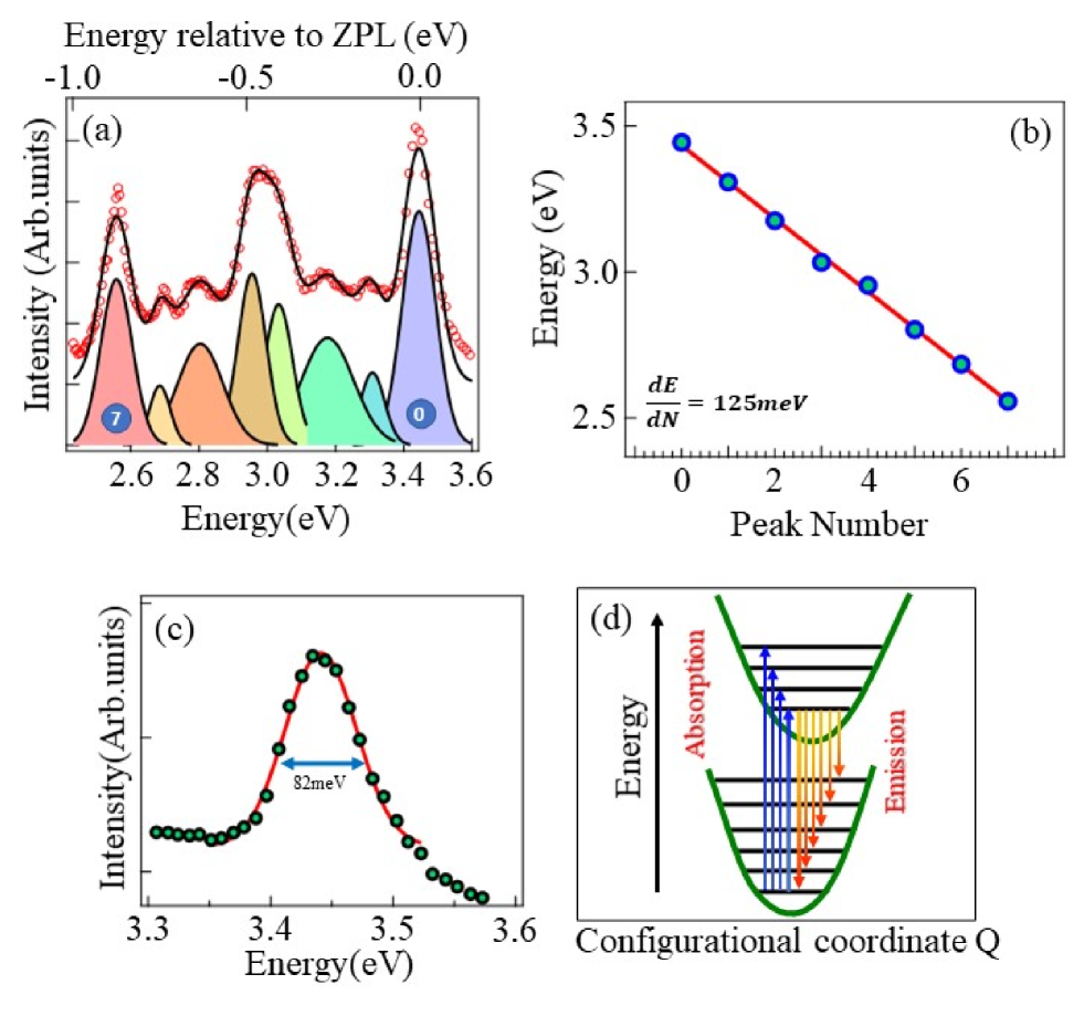
The optical response and the characteristic spectral lines shown from such defects can be modelled using the Franck - Condon (FC-type) type of spectrum. It is well known that in the case of an atomic systems or molecular system, the localised energy levels can strongly couple with optical phonons thereby causing the excitation (absorption) and de-excitation (emission) processes. The excitation caused due to incident light transfers electrons to the excited state while simultaneously annihilating and creating phonons. Such an interpretation has successfully explained the optical transitions between the defect states, notably the nitrogen vacancy (NV center) in diamond. The electronic excitation can couple with the phonons giving rise to phonon side band. The occurrence of phonon side band can also due to the localised modes of the defects in the lattice. Our measurements are done at room temperature, so the spectral features observed will be broad. In the FC-type molecular excitation, the highest energy transition which does not involve phonons is considered as zero-phonon line (ZPL) and in our case it is at 3.44 eV. The asymmetric zero phonon line is plotted in Fig.(5c) shows a very sharp intensity even though measured at room temperature. The FWHM matches very well with the measured values at low temperatures. One of the methods in which the FC-type defect emission is characterised is by calculating the Debye - Waller(DW) factor and Huang-Rys (HR) factors. The DW factor is experimentally found by using the photoluminescence spectrum. It is calculated by taking the ratio of the ZPL and the overall spectrum. Debye - Waller factor is a measure of the electron - phonon coupling strength in the material. From the ZPL3.44 peak, the Debye - Waller factor can be calculated using spectral weight of the ZPL peak and overall emission in the ZPL3.44 band. We obtain a DW factor as 22%. this is reasonable as our measurements are done at room temperature and the calculations of DW factor will contain the thermal broadening of the ZPL3.44 peak which will tend to result in a larger ratio. These quality factors are fairly good considering the procedure adopted for synthesis of the h-BN layers. The corresponding Huang-Rys factor S = -(w) is about 2.08 0.1. The calculation of the RH factor based on our room temperature measurements agree very well with the low temperature measurements.
2.2 conclusions
Understanding the defect structure in h-BN paves the way to fabricate single photon source with well defined emission wavelengths. The synthesis of such a photon source should be easy and cost effective. Here, Multilayer hexagonal boron nitride (h-BN) is prepared using a facile synthesis method which involves heating the precursors in an ambient conditions. A detailed analysis of the XRD pattern reveals that the optimized heating procedure indeed yielded a clean h-BN. Further, the UV-vis spectra shows energy gap ( 5.28 eV) comparable to the reported values in literature. The process induced defects show light emission in the DUV region which is also very essential for the quantum communication in DUV region. We find two type of defects in our samples emitting a DUV light at 4.18 eV and UV light at 3.44 eV. We attribute these two defects to the nitrogen vacancies created during the synthesis of h-BN. The defect with ZPL at 3.44 eV shows a very sharp spectral line even at room temperature. This is associated with a phonon band with equally separated in energy levels. These spectral lines can be explained by considering the excitation-deexcitation process using the Franck - Condon principle. Harmonic oscillator approximation is utilised and the energy level separation is found to be about 125 meV at room temperature. The quality factors are calculated by using the cumulative areas of the spectral lines and the quality factors match very well with that of exfoliated h-BN layers. Our synthesis method is an easy-to-do route to prepare high quality h-BN with deep UV emitting defects, which are useful in the DUV-photonic applications and quantum computation.
Ashley Sunny and R.Thamankar would like to thank Vellore Institute of Technology for their support during this research work. R.Thamankar acknowledges the support of Dr. RG from BITS Hyderabad for the XPS measurements. RT would like to acknowledge Dr. Rajagopal Department of Chemistry, VIT Vellore for critical reading of the manuscript.
Information, which should use the {suppinfo}
-
•
Figure S1.: The reaction scheme of hexagonal Boron Nitride preparation.
-
•
Figure S2.: The excitation wavelength dependence of PL at lower wavelength region.
-
•
Figure S3.: Emission spectra using two solvents, H2O and CH3OH. .
References
- Castro Neto et al. 2009 Castro Neto, A. H.; Guinea, F.; Peres, N. M. R.; Novoselov, K. S.; ; Geim, A. K. The electronic properties of graphene. Reviews of Modern Physics 2009, 81, 109
- Novoselov et al. 2004 Novoselov, K.; Geim, A.; Morozov, S.; Jiang, D.; Zhang, Y.; Dubonos, S.; Grigorieva, I.; Firsov, A. Electric Field Effect in Atomically Thin Carbon Films. Science 2004, 306, 666
- Geim and Novoselov 2007 Geim, A.; Novoselov, K. The rise of graphene. Nat. Mater. 2007, 6, 183
- Mak et al. 2010 Mak, K. F.; Lee, C.; Hone, J.; Shan, J.; Heinz, T. F. Atomically Thin : A New Direct-Gap Semiconductor. Physical Review Letters 2010, 105, 136805
- Bhimanapati et al. 2015 Bhimanapati, G. R. et al. Recent Advances in Two-Dimensional Materials beyond Graphene. ACS Nano 2015, 9, 11509
- Splendiani et al. 2010 Splendiani, A.; Sun, L.; Zhang, Y.; Li, T.; Kim, J.; Chim, C. Y.; Galli, G.; Wang, F. Emerging Photoluminescence in Monolayer MoS2. Nano Letters 2010, 10, 1271
- Eda et al. 2011 Eda, G.; Yamaguchi, H.; Voiry, D.; Fujita, T.; Chen, M.; Chhowalla, M. Photoluminescence from Chemically Exfoliated MoS2. Nano Letters 2011, 11, 5111
- Novoselov et al. 2016 Novoselov, K. S.; Mishchenko, A.; Carvalho, A.; Castro Neto, A. H. 2D materials and van der Waals heterostructures. Science 2016, 353, 9439
- Gibertini et al. 2019 Gibertini, M.; Koperski, M.; Morpurgo, A. F.; Novoselov, K. S. Magnetic 2D materials and heterostructures. Nature Nanotechnology 2019, 14, 408
- Radisavljevic et al. 2011 Radisavljevic, B.; Radenovic, A.; Brivio, J.; Giacometti, V.; Kis, A. Single-layer MoS2 transistors. Nature Nanotechnology 2011, 6, 147
- Castellanos-Gomez et al. 2015 Castellanos-Gomez, A.; Cappelluti, E.; Roldán, R.; Agraït, N.; Guinea, F.; Rubio-Bollinger, G. Electric-Field Screening in Atomically Thin Layers of MoS2: the Role of Interlayer Coupling. Advanced Materials 2015, 25, 899
- Wang et al. 2012 Wang, Q. H.; Kalantar-Zadeh, K.; Kis, A.; Coleman, J. N.; Strano, M. S. Electronics and optoelectronics of two-dimensional transition metal dichalcogenides. Nature Nanotechnology 2012, 7, 699
- Sangwan and Hersam 2018 Sangwan, V. K.; Hersam, M. C. Electronic Transport in Two-Dimensional Materials. Annual Review of Physical Chemistry 2018, 69, 299
- Sun et al. 2018 Sun, Y.; Luo, S.; Zhao, X.-G.; Biswas, K.; Li, S.-L.; Zhang, L. InSe: a two-dimensional material with strong interlayer coupling. Nanoscale 2018, 10, 7991
- Kubota et al. 2007 Kubota, Y.; Watanabe, K.; Tsuda, O.; Taniguchi, T. Deep Ultraviolet Light-Emitting Hexagonal Boron Nitride Synthesized at Atmospheric Pressure. Science 2007, 317, 932
- Museur et al. 2008 Museur, L.; Feldbach, E.; Kanaev, A. Defect-related photoluminescence of hexagonal boron nitride. Physical Review B 2008, 78, 155204
- Watanabe and Taniguchi 2011 Watanabe, K.; Taniguchi, T. Hexagonal Boron Nitride as a New Ultraviolet Luminescent Material and Its Application. International Journal of Applied Ceramic Technology 2011, 8, 977
- Baranov et al. 2011 Baranov, P. G.; Bundakova, A. P.; Soltamova, A. A.; Orlinskii, S. B.; Borovykh, I. V.; Zondervan, R.; Verberk, R.; Schmidt, J. Silicon vacancy in SiC as a promising quantum system for single-defect and single-photon spectroscopy. Physical Review B 2011, 83, 125203
- Koehl et al. 2011 Koehl, W. F.; Buckley, B. B.; Heremans, F. J.; Calusine, G.; Awschalom, D. D. Room temperature coherent control of defect spin qubits in silicon carbide. Nature 2011, 479
- Balasubramanian et al. 2009 Balasubramanian, G.; Neumann, P.; Twitchen, D.; Markham, M.; Kolesov, R.; Mizuochi, N.; Isoya, J.; Achard, J.; Beck, J.; Tissler, J.; Jacques, V.; Hemmer, P. R.; Jelezko, F.; Wrachtrup, J. Ultralong spin coherence time in isotopically engineered diamond. Nature Materials 2009, 8, 383
- Dzurak 2011 Dzurak, A. Diamond and silicon converge. Nature 2011, 479, 47–48
- Pakdel et al. 2012 Pakdel, A.; Zhi, C.; Bando, Y.; Golberg, D. Low-dimensional boron nitride nanomaterials. Materials Today 2012, 15, 256
- Cassabois et al. 2016 Cassabois, G.; Valvin, P.; Gil, B. Hexagonal boron nitride is an indirect bandgap semiconductor. Nature Photonics 2016, 10, 262
- Watanabe et al. 2004 Watanabe, K.; Taniguchi, T.; Kanda, H. Direct-bandgap properties and evidence for ultraviolet lasing of hexagonal boron nitride single crystal. Nature Mater. 2004, 3, 404–409
- Xu and Ching 1991 Xu, Y.-N.; Ching, W. Y. Calculation of ground-state and optical properties of boron nitrides in the hexagonal, cubic, and wurtzite structures. Phys. Rev. B 1991, 44, 7787–7798
- Furthmueller et al. 1994 Furthmueller, J.; Hafner, J.; Kresse, G. Ab initio calculation of the structural and electronic properties of carbon and boron nitride using ultrasoft pseudopotentials. Phys. Rev. B 1994, 50, 15606–15622
- Blase et al. 1995 Blase, X.; Rubio, A.; Louie, S. G.; Cohen, M. L. Quasiparticle band structure of bulk hexagonal boron nitride and related systems. Phys. Rev. B 1995, 51, 6868–6875
- Arnaud et al. 2006 Arnaud, B.; Lebègue, S.; Rabiller, P.; Alouani, M. Huge excitonic effects in layered hexagonal boron nitride. Phys. Rev. Lett. 2006, 96, 026402
- Evans et al. 2008 Evans, D. A.; McGlynn, A. G.; Towlson, B. M.; Gunn, M.; Jones, D.; Jenkins, T. E.; Winter, R.; Poolton, N. R. J. Determination of the optical band-gap energy of cubic and hexagonal boron nitride using luminescence excitation spectroscopy. J. Phys. Condens. Matter 2008, 20, 075233
- Elias et al. 2019 Elias, C.; Valvin, P.; Pelini, T.; Summerfield, A.; Mellor, C. J.; Cheng, T. S.; Eaves, L.; Foxon, C. T.; Beton, P. H.; Novikov, S. V.; Gil, B.; Cassabois, G. Direct band-gap crossover in epitaxial monolayer boron nitride. Nature Communications 2019, 10, 2639
- Tran et al. 2016 Tran, T. T.; Bray, K.; Ford, M. J.; Toth, M.; Aharonovich, I. Quantum emission from hexagonal boron nitride monolayers. Nature Nanotechnology 2016, 11, 37
- Tran et al. 2016 Tran, T. T.; Elbadawi, C.; Totonjian, D.; Lobo, C. J.; Grosso, G.; Moon, H.; Englund, D.; Ford, M. J.; Aharonovich, I.; Toth, M. Robust Multicolor Single Photon Emission from Point Defects in Hexagonal Boron Nitride. ACS Nano 2016, 10, 7331
- Toth and Aharonovich 2019 Toth, M.; Aharonovich, I. Single Photon Sources in Atomically Thin Materials. Annu. Rev. Phys. Chem. 2019, 70, 123
- Gil et al. 2020 Gil, B.; Cassabois, G.; Cusco, R.; Fugallo, G.; Artus, L. Boron nitride for excitonics, nano photonics, and quantum technologies. Nanophotonics 2020, 9, 3483–3504
- Exarhos et al. 2019 Exarhos, A. L.; Hopper, D. A.; Patel, R. N.; Doherty, M. W.; Bassett, L. C. Magnetic-field-dependent quantum emission in hexagonal boron nitride at room temperature. Nature Communications 2019, 10
- Ferreira et al. 2019 Ferreira, F.; Chaves, A. J.; Peres, N. M. R.; Ribeiro, R. M. Excitons in hexagonal boron nitride single-layer: a new platform for polaritonics in the ultraviolet. Journal of the Optical Society of America B 2019, 36, 674–683
- Ba et al. 2017 Ba, K.; Jiang, W.; Cheng, J.; Bao, J.; Xuan, N.; Sun, Y.; Liu, B.; Xie, A.; Wu, S.; Sun, Z. Chemical and Bandgap Engineering in Monolayer Hexagonal Boron Nitride. Scientific Reports 2017, 7, 45584
- Román et al. 2021 Román, R. J. P.; Costa, F. J. R. C.; Zobelli, A.; Elias, C.; Valvin, P.; Cassabois, G.; Gil, B.; Summerfield, A.; Cheng, T. S.; Mellor, C. J.; Beton, P.; Novikov, S.; Zagonel, L. F. Band gap measurements of monolayer h-BN and insights into carbon-related point defects. 2D Materials 2021, 8, 044001
- Park et al. 2017 Park, H.; Kim, T.; Cho, S. W.; Jang, H. S.; Lee, S.; Choi, S.-Y. Large-scale synthesis of uniform hexagonal boron nitride films by plasma-enhanced atomic layer deposition. Scientific Reports 2017, 7, 40091
- Kim et al. 2012 Kim, K. K.; Hsu, A.; Jia, X.; Kim, S. M.; Shi, Y.; Hofmann, M.; Nezich, D.; Rodriguez-Nieva, J. F.; Dresselhaus, M.; Palacios, T.; Kong, J. Synthesis of Monolayer Hexagonal Boron Nitride on Cu Foil Using Chemical Vapor Deposition. Nano Letters 2012, 12, 161–166
- Pierucci et al. 2018 Pierucci, D.; Zribi, J.; Henck, H.; Chaste, J.; Silly, M. G.; Bertran, F.; Le Fevre, P.; Gil, B.; Summerfield, A.; Beton, P. H.; Novikov, S. V.; Cassabois, G.; Rault, J. E.; Ouerghi, A. Van der Waals epitaxy of two-dimensional single-layer h-BN on graphite by molecular beam epitaxy: Electronic properties and band structure. Applied Physics Letters 2018, 112, 253102
- Jin et al. 2009 Jin, C.; Lin, F.; Suenaga, K.; Iijima, S. Fabrication of a Freestanding Boron Nitride Single Layer and Its Defect Assignments. Physical Review Letters 2009, 102, 195505
- Weber et al. 2010 Weber, J. R.; Koehl, W. F.; Varley, J. B.; Janotti, A.; Buckley, B. B.; Van de Walle, C. G.; Awschalom, D. D. Quantum computing with defects. Proceedings of the National Academy of Sciences 2010, 107, 8513
- Gupta et al. 2019 Gupta, S.; Yang, J. H.; Yakobson, B. I. Two-Level Quantum Systems in Two-Dimensional Materials for Single Photon Emission. Nano Letters 2019, 19, 408–414
- Frey et al. 2020 Frey, N. C.; Akinwande, D.; Jariwala, D.; Shenoy, V. B. Machine Learning-Enabled Design of Point Defects in 2D Materials for Quantum and Neuromorphic Information Processing. ACS Nano 2020, 14, 13406–13417
- Wolters et al. 2010 Wolters, J.; Schell, A. W.; Kewes, G.; Nüsse, N.; Schoengen, M.; Döscher, H.; Hannappel, T.; Löchel, B.; Barth, M.; Benson, O. Enhancement of the zero phonon line emission from a single nitrogen vacancy center in a nanodiamond via coupling to a photonic crystal cavity. Applied Physics Letters 2010, 97, 141108
- Klein et al. 2020 Klein, J. et al. Engineering the Luminescence and Generation of Individual Defect Emitters in Atomically Thin MoS2. ACS Photonics 2020, 8, 669–677
- Ranjan et al. 2021 Ranjan, A.; Raghavan, N.; Holwill, M.; Watanabe, K.; Taniguchi, T.; Novoselov, K. S.; Pey, K. L.; O’Shea, S. J. Dielectric Breakdown in Single-Crystal Hexagonal Boron Nitride. ACS Applied Electronic Materials 2021, 3, 3547–3554
- Li et al. 2016 Li, J.; Cao, X. K.; Hoffman, T. B.; Edgar, J. H.; Lin, J. Y.; Jiang, H. X. Nature of exciton transitions in hexagonal boron nitride. Applied Physics Letters 2016, 108, 122101
- Matović et al. 2016 Matović, B.; Luković, J.; Nikolić, M.; Babić, B.; Stanković, N.; Jokić,; Jelenković, B. Synthesis and characterization of nanocrystaline hexagonal boron nitride powders: XRD and luminescence properties. Ceramics International 2016, 42, 16655–16658
- Paine and Narula 1990 Paine, R. T.; Narula, C. K. Synthetic routes to boron nitride. Chemical Reviews 1990, 90, 73–91
- Lee and Song 2017 Lee, D.; Song, S. H. Ultra-thin ultraviolet cathodoluminescent device based on exfoliated hexagonal boron nitride. RSC Advances 2017, 7, 7831
- Balapure et al. 2020 Balapure, A.; Nikhariya, Y.; Sriteja Boppudi, N. S.; Ganesan, R.; Ray Dutta, J. Highly Dispersed Nanocomposite of AgBr in g-C3N4 Matrix Exhibiting Efficient Antibacterial Effect on Drought-Resistant Pseudomonas putida under Dark and Light Conditions. ACS Applied Materials Interfaces 2020, 12, 21481–21493
- Moulder et al. 1992 Moulder, J., Stickle, W., Sobol, P., Eds. Handbook of X-ray Photoelectron Spectroscopy, illustrated ed.; Physical Electronics Division, Perkin-Elmer Corporation,: Minnesota, 1992
- Marini et al. 2006 Marini, A.; García-González, P.; Rubio, A. First-Principles Description of Correlation Effects in Layered Materials. Physical Review Letters 2006, 96, 136404
- Marom et al. 2010 Marom, N.; Bernstein, J.; Garel, J.; Tkatchenko, A.; Joselevich, E.; Kronik, L.; Hod, O. Stacking and Registry Effects in Layered Materials: The Case of Hexagonal Boron Nitride. Physical Review Letters 2010, 105, 046801
- 57 Sainsbury, T.; Satti, A.; May, P.; Wang, Z.; McGovern, I.; Gun’ko, Y. K.; Coleman, J.
- Bhimanapati et al. 2014 Bhimanapati, G. R.; Kozuch, D.; Robinson, J. A. Large-scale synthesis and functionalization of hexagonal boron nitride nanosheets. Nanoscale 2014, 6, 11671–11675
- Khorasani et al. 2021 Khorasani, E.; Frauenheim, T.; Aradi, B.; Deák, P. Identification of the Nitrogen Interstitial as Origin of the 3.1eV Photoluminescence Band in Hexagonal Boron Nitride. physica status solidi (b) 2021, 258, 2100031
- Attaccalite et al. 2011 Attaccalite, C.; Bockstedte, M.; Marini, A.; Rubio, A.; Wirtz, L. Coupling of excitons and defect states in boron-nitride nanostructures. Physical Review B 2011, 83, 144115
- Sajid et al. 2020 Sajid, A.; Reimers, J. R.; Kobayashi, R.; Ford, M. J. Theoretical spectroscopy of the defect in hexagonal boron nitride. Physical Review B 2020, 102, 144104
- Sajid et al. 2020 Sajid, A.; Ford, M. J.; Reimers, J. R. Single-photon emitters in hexagonal boron nitride: a review of progress. Reports on Progress in Physics 2020, 83, 044501
- Hamdi et al. 2020 Hamdi, H.; Thiering, G.; Bodrog, Z.; Ivády, V.; Gali, A. Stone–Wales defects in hexagonal boron nitride as ultraviolet emitters. npj Computational Materials 2020, 6, 178
- Weston et al. 2018 Weston, L.; Wickramaratne, D.; Mackoit, M.; Alkauskas, A.; Van de Walle, C. G. Native point defects and impurities in hexagonal boron nitride. Physical Review B 2018, 97, 214104
- Tsushima et al. 2018 Tsushima, E.; Tsujimura, T.; Uchino, T. Enhancement of the deep-level emission and its chemical origin in hexagonal boron nitride. Applied Physics Letters 2018, 113, 031903
- Gribkovskii and Vij 1998 Gribkovskii, V. P., Vij, V. R., Eds. Luminescence of Solids; Springer US: New York, 1998
- Reich et al. 2005 Reich, S.; Ferrari, A. C.; Arenal, R.; Loiseau, A.; Bello, I.; Robertson, J. Resonant Raman scattering in cubic and hexagonal boron nitride. Physical Review B 2005, 71, 205201
- Berzina et al. 2016 Berzina, B.; Korsaks, V.; Trinkler, L.; Sarakovskis, A.; Grube, J.; Bellucci, S. Defect-induced blue luminescence of hexagonal boron nitride. Diamond and Related Materials 2016, 68, 131–137