Nonlinear optical Hall effect of few-layered NbSe2
Abstract
NbSe2 is one of metallic two-dimensional (2D) transition-metal dichalcogenide (TMDC) materials. Because of broken crystal inversion symmetry, large spin splitting is induced by Ising-type spin-orbit coupling in odd-number-layered NbSe2, but absent for even-number-layered NbSe2 with the inversion symmetry. In this paper, we numerically calculate nonlinear optical charge and spin Hall conductivities of few-layered NbSe2 based on an effective tight-binding model which includes , and orbitals of Nb atom. We show that the nonlinear optical Hall conductivity for second harmonic generation (SHG) process has nonvanishing value in odd-number-layered NbSe2. Also, we provide nonlinear optical selection rule in few-layered NbSe2 and their polarization dependences. In further, for even-number-layered case, the nonlinear optical Hall currents can be generated by applying electric fields which breaks inversion symmetry. We also discuss that the nonlinear optical Hall effect is expected to occur in TMDC materials in general. Thus, our results will serve to design potential opt-spintronics devices based on 2D materials to generate the spin Hall current by SHG.
I Introduction
Transition metal dichalcogenide (TMDC) with a chemical formula MX2 (M=Mo, W, Nb, Ta; X=S, Se) is a new class of two-dimensional (2D) electronic systems, which provides the platform to design functional opt-electronic devices. Mak et al. (2010); Splendiani et al. (2010); Tongay et al. (2012); Gutiérrez et al. (2013); Zhao et al. (2013); Ciarrocchi et al. (2018); Samadi et al. (2018); Thakar and Lodha (2020); Wu et al. (2021) Owing to weak van der Waals forces between layers, bulk TMDC can be easily exfoliated into monolayer. Novoselov et al. (2005); Desai et al. (2016); Lin et al. (2016); Yu et al. (2018); Wang et al. (2021) In monolayer MoS2 and WSe2, the valley-dependent optical excitation Zeng et al. (2012); Mak et al. (2012); Cao et al. (2012); Yu et al. (2015) and intrinsic spin Hall effect (SHE) Sinova et al. (2015); Hai (2020); Kato et al. (2004); Wunderlich et al. (2005) have been reported. In further, nonlinear optical effect such as second-harmonic generation (SHG), Wen et al. (2019); Lucas et al. (2021); Taghizadeh and Pedersen (2019); Trolle et al. (2014); Kumar et al. (2013); Moss et al. (1987); Ghahramani et al. (1991); Malard et al. (2013); Seyler et al. (2015); Rashkeev et al. (1998); Rashkeev and Lambrecht (2001); Sharma and Ambrosch-Draxl (2004); Leitsmann et al. (2005) sum-frequency generation (SFG), Shen (1989, 2020); Shultz et al. (2000); Richmond (2002); Shen and Ostroverkhov (2006); Gopalakrishnan et al. (2006); Ishiyama et al. (2014) third-harmonic generation (THG), Wen et al. (2019); Tsang (1995); Squier et al. (1998); Stock et al. (2020) high-harmonic generation (HHG) Wen et al. (2019); Dromey et al. (2006); Winterfeldt et al. (2008); Vampa et al. (2014) and two-photon absorption Wen et al. (2019); Pawlicki et al. (2009); Rumi and Perry (2010); Wang et al. (2020) has been extensively studied. In general, the nonlinear optical effect is sensitive to crystal symmetries and phase-matching conditions between incident light and light-induced electric polarization wave. However, the phase-matching conditions are not necessary for nonlinear optical effect in atomically-thin 2D materials, because their thickness is much smaller than the light wavelength. Wen et al. (2019); Fryett et al. (2017); He et al. (2021) Thus, in atomically-thin 2D materials such as TMDCs, the nonlinear optical effect strongly depends on the crystal symmetry. In addition, it has been recently discussed that second-order anomalous transport phenomena in the absence of magnetic field can be induced by uniaxial strain in metallic TMDC, i.e., nonlinear Hall effect, which has a relation with Berry curvature dipole. Xiao et al. (2020); Zhou et al. (2020); Ma et al. (2019); Sodemann and Fu (2015)
NbSe2 is metallic TMDC which shows superconducting phase transition at low temperatures. Wilson et al. (2001); Kim and Son (2017); He et al. (2018); Xi et al. (2016); Sohn et al. (2018a); Anikin et al. (2020); Lian et al. (2017) In this material, AB-stacking structure is most stable in nature and has different crystal symmetries for even and odd number of layers. In even-number-layered NbSe2, the crystal structure has a space group D3d, which respects to inversion and out-of-plane mirror symmetries. On the other hand, odd-number-layered NbSe2 has a space group D3h, which possesses out-of-plane mirror symmetry, but no spacial inversion symmetry. Because of the broken inversion symmetry and a strong spin-orbit coupling (SOC) field of Nb atoms in odd-number-layered NbSe2, it possesses Ising-type SOC, He et al. (2018); Xi et al. (2016); Sohn et al. (2018a); Lu et al. (2015); Saito et al. (2016); Zhou et al. (2016); Bawden et al. (2016) i.e., an effective Zeeman field that locks electron spins to out-of-plane directions by in-plane momentum and causes larger spin splitting in the energy band structures leading to unconventional topological spin properties. In actual, we have analyzed the linear optical properties of monolayer NbSe2 using Kubo formula based on an effective tight-binding model (TBM) and shown that the spin Hall current can be induced by irradiating visible light owing to its finite spin Berry curvature. Habara and Wakabayashi (2021)
In this paper, we extend our theoretical analysis to nonlinear optical spin and charge Hall conductivities of SHG process for few-layered NbSe2. Here, we have employed the effective TBM to describe the electronic structures of few-layered NbSe2, where the electron hoppings among , and orbitals of Nb atom and Ising-type SOC are included. Numerical calculation shows that owing to the broken inversion symmetry, the nonlinear optical Hall currents are generated in odd-number-layered NbSe2, but absent for even-number-layered NbSe2. In particular, under irradiating -polarized visible light, nonlinear spin Hall current appears. On the other hand, the -polarized visible light generates nonlinear charge Hall current. In further, for even-number-layered NbSe2, the spin and charge Hall current can be generated if the out-of-plane mirror and inversion symmetries are broken by the application of electric fields perpendicular to the plane. Thus, we provide nonlinear optical selection rule of spin and charge Hall currents in few-layered NbSe2, which clarifies the even-odd effect of layer numbers and light polarization dependencies. Our results will serve to design potential opt-spintronics devices on the basis of 2D materials.
This paper is organized as follows. In Sec. II, we discuss effective model of even- and odd-number-layered NbSe2 which includes crystal structure and energy band structure. In Sec. III, we numerically calculate nonlinear optical spin and charge Hall conductivities for alternating current (AC) fields and find that the nonlinear optical Hall currents strongly depend on layer numbers and polarization of incident light. In Sec. IV, we discuss that when the crystal symmetry is broken by applying electric fields, nonlinear optical Hall currents can be generated even in even-number-layered NbSe2. In Sec. V, we summarize our results. In addition, in Appendix we show details of matrix elements in an effective Hamiltonian. Also, we present contour plots of integrands for nonlinear optical spin and charge Hall conductivities and energy band structures of bilayer NbSe2 with the application of electric fields. In Supplementary Material, we provide the details of the 2nd order nonlinear optical conductivities, temperature effect for odd-number-layered NbSe2 and nonlinear optical Hall conductivity of monolayer MoS2 as a reference example of TMDC semiconductor. sup
II Model
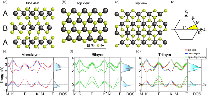
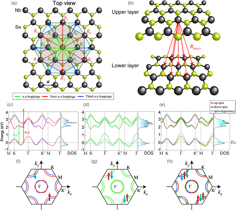
In this paper, we show that nonlinear optical spin and charge currents of few-layered NbSe2 strongly depend on the crystal symmetry and number of stacking layers. Especially, we focus on the cases of monolayer, AB-stacked bilayer and ABA-stacked trilayer NbSe2. Figure 1 (a) shows schematic of few-layered NbSe2 with AB stacking, which is the most energetically stable stacking sequence in NbSe2. Each layer has the out-of-plane mirror symmetry with respect to the plane of Nb atoms. Figures 1 (b) and (c) show the top views of monolayer NbSe2 and AB-stacked few-layered NbSe2, respectively. In even-number-layered case, NbSe2 has a space group D3d, which respects to inversion symmetry. However, in case of odd-number-layered NbSe2, it has a space group D3h, which has no spatial inversion symmetry. Figure 1 (d) shows first Brillouin Zone (BZ) for few-layered NbSe2.
We employ a multi-orbitals TBM which includes , and orbitals of Nb atom to describe the electronic states of NbSe2. He et al. (2018); Liu et al. (2013); Habara and Wakabayashi (2021) The eigenvalue equation for TBM is where is the wave-number vector, is the eigenvalue and ( is number of layer) is the band index. The eigenvector is defined as , where indicates the transpose of vector and means the amplitude at atomic orbital with spin for the th energy band at . The Hamiltonian of monolayer NbSe2 with the SOC can be written as
| (1) |
with
| (2) |
and
| (3) |
Here, and are Pauli matrices and is the Ising-type SOC parameter. In monolayer NbSe2, eV. includes the electron hoppings only among three -orbitals of Nb atoms, which are assumed up to third-nearest neighbor sites as shown in Appendix A. Similarly, Hamiltonians of bilayer and trilayer NbSe2 can be obtained as
| (4) |
and
| (5) |
respectively. Sohn et al. (2018b) Here, interlayer coupling Hamiltonian is considered as
| (6) |
The details of matrix elements , , , , , , and can be found in Appendix A.
Figures 1 (e), (f) and (g) show the energy band structures of monolayer, bilayer and trilayer NbSe2 together with the corresponding density of states (DOS), respectively. Here, red, blue and green lines indicate spin-up, spin-down and spin-degenerated states. NbSe2 is metallic, but a large energy band gap between the partially filled valence bands and empty conduction bands. Also, opposite spin splitting in the energy band structure can be seen at the valence band edges in K and K′ points in monolayer NbSe2 owing to the broken inversion symmetry. However, because even-number-layered NbSe2 such as bilayer respect the inversion symmetry, it does not show the spin splitting. It should be noted that even-number-layered NbSe2 has larger band splitting at valence band in point, becase the interlayer interaction becomes larger in point than in K and K′ points. Figure 1 (g) shows the calculated energy band structure of trilayer NbSe2, which can be understood by overwriting spin degenerated energy band structure of bilayer NbSe2 onto that of spin-splitting energy dispersion of monolayer NbSe2. Since the inversion symmetry is broken in odd-number-layered NbSe2, spin degeneracy is lifted. However, owing to the existence of spin degenerated energy band of bilayer NbSe2, the spin splitting at K and K′ points is not clearly seen. The details of Fermi spin-dependent surface structures are shown in Appendix A.
III Nonlinear optical Hall conductivity
| nonlinear optical spin conductivity | nonlinear optical charge conductivity | |
| mono (D3h) | ||
| bi (D3d) | zero | zero |
| tri (D3h) | ||
We numerically calculate nonlinear optical spin and charge Hall conductivities for few-layered NbSe2 based on an effective TBM. In general, the 2nd order nonlinear optical spin conductivity can be given as Kang and Choi (2010); Lee et al. (2002); Kang and Choi (2012); Kang et al. (2013); Moss et al. (1987); Ghahramani et al. (1991); Rashkeev and Lambrecht (2001); Leitsmann et al. (2005); Aversa and Sipe (1995); Sipe and Ghahramani (1993)
| (7) |
with
| (8) |
where is integrand of nonlinear optical spin conductivity. Here, (, ) indicates the direction or . In particular, is the generation direction of nonlinear optical spin current, and () is polarization of incident light. Also, (, ) is the band index including spin degree of freedom, is the eigen function with the eigen energy and is Fermi-Dirac distribution function. , and means the th frequency mode. is infinitesimally small real number and is the area of system. Moreover, is the spin current operator and written as , where is the identity matrix and is used for monolayer, bilayer and trilayer NbSe2, respectively. Here, is the group velocity operator. The nonlinear optical charge conductivity is also obtained by changing to which is defined as . We add the superscript “” for the nonlinear optical spin conductivity in order to distinguish its conductivity from the nonlinear optical charge conductivity. In case of , the process is called as SFG [see Figs. S3]. sup Especially, in case of , the process is called as SHG. Also, in case of , the process is called as difference frequency generation (DFG). Lu et al. (2011); Axel et al. (2012) Since we have interest in SHG, we focus on the SHG process in this manuscript, i.e. .
The 2nd order nonlinear optical conductivity expressed by Eq. (7) can be separated into two inter-band processes: (i) optical transition between two bands and (ii) optical transition involving three bands . Aversa and Sipe (1995); Passos et al. (2021) Namely, can be decomposed into
| (9) |
The detail of derivation can be found in Appendix B. In particular, considering the inter-band transition between two bands around Fermi surface, can be rewritten as
| (10) |
where is the Berry curavture dipole Zeng et al. (2021); Sodemann and Fu (2015)
| (11) |
Thus, the two-band process is nothing more than the effect of Berry curvature dipole. In the direct current (DC) limit, i.e., , is identically zero in NbSe2. However, it is expected to be finite even in the DC limit, if the uniaxial strain is applied to the system. Zeng et al. (2021); Sodemann and Fu (2015) In this work, we consider regardless of two-bands and three-bands inter-band processes.
Since the nonlinear optical conductivity is the rd rank tensor, in general and have the components, respectively. However, using the Neumann’s principle, Wen et al. (2019); Lucas et al. (2021) we can find the nonvanishing elements of and from the crystal symmetry. Because the inversion symmetry is broken in monolayer NbSe2, the nonvanishing tensor elements are obtained as following:
| (12) |
and
| (13) |
However, owing to the inversion symmetry in even-number-layered NbSe2 such as bilayer NbSe2, the nonlinear optical conductivities are obviously absent, i.e., all the tensor elements are identically zero. Also, since the crystal symmetry of trilayer NbSe2 is identical to the monolayer NbSe2, same relations of the nonlinear optical spin and charge conductivities are obtained using Neumann’s principle. Table 1 summarizes the relations of nonvanishing tensor elements of and for few-layered NbSe2. It should be noted that the nonlinear optical charge conductivity is zero, whenever the nonlinear optical spin conductivity has finite value. Since the 2nd order nonlinear optical conductivity is a complex function of , the conductivity can be separated as
| (14) |
where and are real and imaginary parts, respectively. In the main text, we focus on the real part of . The details of the imaginary part of are shown in Supplementary Material.
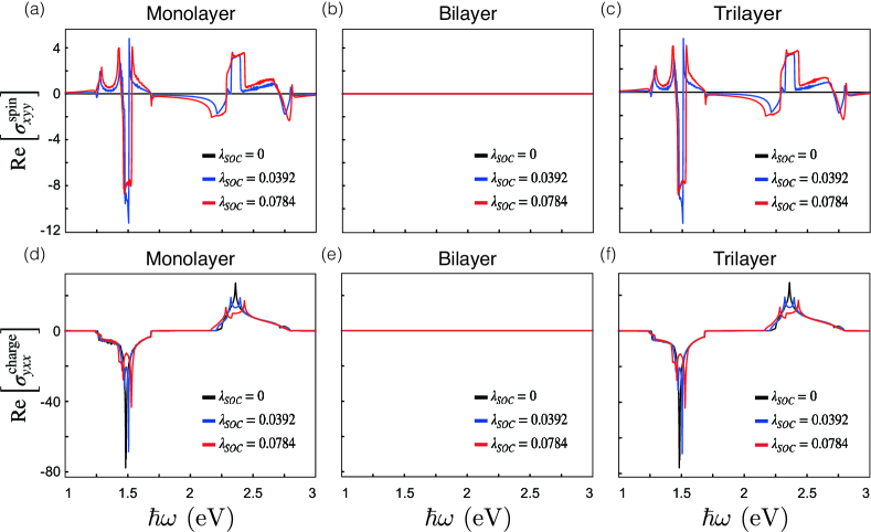
Figures 2 (a), (b) and (c) show the real parts of nonlinear optical spin Hall conductivities of monolayer, bilayer and trilayer NbSe2, respectively. Here, is considered as the case of SHG process and has Ising-type SOC parameter eV. Also, the cases for and eV are plotted for the comparison. represents that the spin Hall current is generated in direction by irradiating polarized light. It mainly has two peaks around and eV for odd-number-layered NbSe2 owing to even-parity with respect to and axes in contour plot of [see Appendix C]. One peak can be seen around eV, and indicates an excitation from valence band to conduction band by one incident photon at . The other peak around eV shows that two incident photons at occurs an excitation from valence band to intermediate band and then conduction band.
Figures 2 (d), (e) and (f) show the real parts of nonlinear optical charge Hall conductivities of SHG process for monolayer, bilayer and trilayer NbSe2, respectively. represents that the charge Hall current is generated in direction by irradiating polarized light. There are mainly two peaks around and eV as same as the case of , which appear for owing to the asymmetry of with respect to axis in contour plot [see Appendix C]. For one incident photon at , one peak appears around eV, and it is larger than the other peak around eV which can be seen by two incident photons at .
Thus, we can find that the nonlinear optical spin and charge Hall currents strongly depend on layer numbers and polarization of incident light in visible range, i.e., nonlinear optical selection rule of spin and charge Hall currents in few-layered NbSe2.
Here we briefly mention the extreme similarity of the nonlinear optical conductivities between monolayer and trilayer NbSe2 as shown in Fig. 2. The trilayer NbSe2 can be viewed as the composite of monolayer and bilayer NbSe2. Therefore, we have three contributions of optical transition processes: (A) intralayer optical transition of monolayer NbSe2, (B) intra- and interlayer optical transition of bilayer NbSe2, and (C) interlayer optical transitions between monolayer and bilayer NbSe2. Since the process (B) is identically zero, the process (A) dominates the optical conductivities of trilayer NbSe2. It is shown that the process (C) is canceled because of band inversion along the -K and -K′ lines in BZ. The detail can be found in Supplementary Material.
Also, we have mentioned that the nonlinear optical Hall conductivity has the peaks (around and eV) corresponding to absorption of two photons in odd-number-layered NbSe2, which cannot be seen for linearly optical Hall conductivity obtained by Kubo formula. Habara and Wakabayashi (2021); Kim and Son (2021) It should be noted that the magnitude of peak clearly corresponds to DOS of NbSe2. The details of these peaks are shown in Supplementary Material.
In addition, TMDC semiconductor such as MoS2 has a pronounced peak around eV in the nonlinear optical Hall conductivity. The details of nonlinear optical Hall conductivity of monolayer MoS2 can be found in Supplementary Material. This transition process corresponds to the SHG process marked with the green arrows in Fig. 5 (c) of Appendix A. Thus, SHG can be expected in the doped MoS2. Similarly, when we consider the case of electron-doped NbSe2 to make the valence bands fully occupied, the system behaves as a semiconductor. In this case, the nonlinear optical conductivity for SHG process has the localized peak around eV (not shown). This transition process also corresponds to the SHG process marked with the green arrows in Fig. 5 (c) of Appendix A, which is same as the case of MoS2.
In previous works, Xiao et al. (2020); Zhou et al. (2020); Ma et al. (2019); Sodemann and Fu (2015) it is reported that the nonlinear charge Hall current in DC limit can be generated even in the absence of magnetic field, by considering monolayer NbSe2 under uniaxial strain or hole-doped semiconductor TMDC. These results can be induced by Berry curvature dipole which provides unconventional behavior, i.e., nonlinear Hall effect, but it is limited to in metallic TMDC. In this work, however, we can show that the nonlinear charge Hall current appears in not only metallic TMDC but also semiconductor TMDC by light irradiation even without SOC and uniaxial strain [see Figs. 2 (d) and (f)]. Thus, we can generate the nonlinear charge Hall current simply by irradiating light in few-layered NbSe2 without the external perturbations such as magnetic field, strain and carrier dopings.
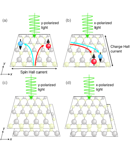
Figure 3 summarizes the schematics of nonlinear optical Hall currents in few-layered NbSe2 which capture the results of Fig. 2. Figure 3 (a) indicates that nonlinear optical spin Hall current is generated in direction by irradiating polarized light in odd-number-layered NbSe2. However, nonlinear optical charge Hall current is absent. Figure 3 (b) shows that nonlinear optical charge Hall current is generated in direction by irradiating polarized light, but then the spin Hall current is absent. Also, Figures 3 (c) and (d) show that because even-number-layered NbSe2 respects to inversion symmetry, the nonlinear optical spin and charge Hall currents are identically zero.
IV Electric field effect of nonlinear optical Hall conductivity
Since the application of electric field perpendicular to the plane breaks the crystal inversion symmetry in bilayer NbSe2, the nonlinear optical spin and charge Hall conductivities can be generated even in bilayer NbSe2 with the application of electric field. Figure 4 (a) shows the real part of nonlinear optical spin Hall conductivity of bilayer NbSe2 for several different applied electric fields. Here, black, blue, cyan, green, yellow, purple and red lines indicate the applied electric fields: , , , , , and eV, respectively. We can see peaks of around and eV as same as the case of odd-number-layer. In addition, there is a pronounced peak which shifts toward higher frequency with increase of electric field, which is indicated by the dashed square in Fig. 4 (a). The peak is originated from the interlayer optical absorption. Since the energy bands of upper (lower) layer shift toward higher (lower) energy, the energy difference between upper and lower layers increases with increase of electric field, resulting in the shift of interlayer optical absorption peak. The details about energy band structures of bilayer NbSe2 with applied electric fields and its parity between layers are shown in Appendix D.
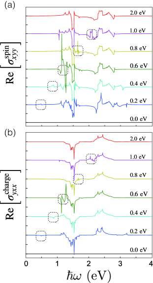
Figure 4 (b) shows the real part of nonlinear optical charge Hall conductivity of bilayer NbSe2 with applied electric fields. Because of the broken crystal inversion symmetry in even-number-layered NbSe2 with applied electric fields, the nonlinear optical charge Hall current can be generated by irradiating polarized light. also has peaks around and eV, which is similar to the case of . Similarly, we can observe the frequency shift of interlayer optical absorption peak which is indicated by the dashed squares. Thus, we can indicate that owing to the broken inversion symmetry in even-number-layered NbSe2 with applied electric fields, the nonlinear optical spin and charge Hall currents can be generated by irradiating visible light.
Instead of the application of electric fields to NbSe2, we consider the nonlinear optical spin and charge conductivities of bilayer NbSe2 with each layer having a different Fermi energy, i.e. decoupled bilayer NbSe2. The details of the nonlinear optical spin and charge Hall conductivities of the decoupled bilayer NbSe2 are shown in Appendix E.
V Conclusion
In conclusion, we have theoretically proposed that nonlinear optical spin and charge Hall currents based on SHG process can be enhanced by irradiating visible light. Also, we have shown that the Hall currents strongly depend on layer numbers, crystal symmetry of NbSe2 and polarization of incident light, i.e., nonlinear optical selection rule of spin and charge Hall currents in few-layered NbSe2. In previous works, it is known that the nonlinear Hall effect is induced in metallic and doped semiconductor TMDCs by uniaxial strain, which depends on the Berry curvature dipole in 1st BZ. In our work, we can find nonlinear Hall effect by light irradiation in NbSe2 and MoS2 with hole-doping, even in the absence of strain. In Supplementaly Material, it is also shown that the nonlinear optical spin and charge Hall conductivities can occur in MoS2 without doping. Thus, in general, it is expected that the nonlinear optical Hall effect can occur in TMDC materials.
In addition, we have found that the nonlinear optical spin and charge Hall currents of few-layered NbSe2 based on the effective TBM are robust to temperature and are expected to be observed even at room temperature [see Supplementary Material].
In this paper, we have found that the oscillating spin and charge Hall current could be induced by the SHG. Though the static charge and spin accumulation does not occur, the polarized spin current can be extracted if we attach the half-metal materials to the edge of the sample as a spin filter.
Thus, few-layered NbSe2 can be used for the source of induced nonlinear optical spin Hall current by SHG. Our results can serve to design opt-spintronics devices on the basis of 2D materials.
Acknowledgements.
This work was supported by JSPS KAKENHI (Nos. JP21H01019, JP18H01154) and JST CREST (No. JPMJCR19T1).Appendix A Matrix elements of few-layered NbSe2
| 1.4466 | 1.8496 | -0.2308 | 0.3116 | 0.3459 | 0.2795 | 0.2787 | -0.0539 | 0.0037 | -0.0997 | 0.0385 |
| 0.0320 | 0.0986 | 0.1233 | -0.0381 | 0.0535 | 0.0601 | -0.0179 | -0.0425 | -0.0179 | -0.0702 | 0.0784 |
We employ a multi-orbitals TBM which includes , and orbitals of Nb atom to describe the electronic states of NbSe2. The eigenvalue equation for TBM is where is the wave-number vector, is the eigenvalue and ( is number of layers) is the band index. The eigenvector is defined as , where indicates the transpose of vector and means the amplitude at atomic orbital with spin for the th energy band at . The Hamiltonian of monolayer NbSe2 with Ising-type SOC can be written as
| (15) |
with
| (16) |
and
| (17) |
Here, and are Pauli matrices and is the Ising-type SOC parameter. In monolayer NbSe2, eV. includes the electron hoppings only among three -orbitals of Nb atoms, which are assumed up to third-nearest neighbor sites as shown in Fig. 5 (a). Here, green, red and blue arrows indicate hopping vectors pointing to nearest-neighbor (n.n) sites, the vectors pointing to next n.n sites and the vectors pointing to third n.n sites, respectively. We can find the matrix elements in the effective TBM Hamiltonian of monolayer NbSe2 Liu et al. (2013); Kim and Son (2021): , , , , and as
| (18) |
| (19) |
| (20) |
| (21) |
| (22) |
| (23) |
| (24) |
| (25) |
and
| (26) |
Here, and the lattice constant is Å. The specific hopping parameters in this TBM can be given as
| (27) |
where indicates an atomic orbital of Nb atom and in this paper, we consider , and . For example, we can express , , , , and .
Similarly, Hamiltonians of (AB-stacked) bilayer and (ABA-stacked) trilayer NbSe2 can be obtained as
| (28) |
and
| (29) |
respectively. In Fig. 5 (b), interlayer hopping vector points -orbital of upper layer to n.n sites of lower layer and the interlayer coupling Hamiltonian is considered as
| (30) |
where and are fitted by using hopping parameters and :
| (31) |
| (32) |
respectively. The details about fitted parameters for this TBM are summarized in Table 2. He et al. (2018)
The energy band structures and DOS are shown in Figs. 5 (c), (d) and (e). Here, red, blue and green lines indicate spin-up, spin-down and spin-degenerated states, respectively. The energy band structure of monolayer NbSe2 is qualitatively similar to heavily hole-doped monolayer MoS2. Unlike monolayer MoS2 which shows semiconducting behavior, monolayer NbSe2 is metallic, but a large energy band gap between the partially filled valence bands and empty conduction bands. Also, the Ising-type SOC provides opposite spin splitting at the valence band edges in K and K′ points, and time-reversal symmetry protection. In particular, the SOC makes the spin splitting about meV at the K point. Figure 5 (d) shows that the spin splitting is absent in the energy band structure of bilayer NbSe2, but larger band splitting appears at valence band in point because of the spacial inversion symmetry. Figure 5 (e) shows that trilayer NbSe2 has spin splitting bands owing to the broken crystal inversion symmetry as same as the case of monolayer. In gneral, the energy band structures of NbSe2 have spin-degeneracy along the -M line, which can be confirmed by looking at Fermi surface structure. Also, this is because the Hamiltonians for up- and down-spin states have the following properties: , and , respectively. Since we have interest in the SHG, we discuss the nonlinear optical conductivity for SHG process (). Figure 5 (c) includes the two SHG processes: (i) inter-band transition by two-photon absorption (green arrows) and (ii) inter-band transition even by one-photon absorption (red arrows).
Figure 5 (f) shows Fermi surface of monolayer NbSe2. The surface has Fermi pockets centered at , K and K′ points, which show the spin-splitting. Also, because of the opposite spin-splitting around K and K′ points, the energy band structure of monolayer NbSe2 is anisotropic with respect to point. Figure 5 (g) indicates Fermi surface of bilayer NbSe2. Unlike the case of monolayer, the surface has spin-degenerated Fermi pockets owing to the crystal inversion symmetry. Figure 5 (h) shows Fermi surface of trilayer NbSe2, which has spin-splitting Fermi surface. This Fermi surface can be understood by overlaying the spin-splitting Fermi surface of monolayer NbSe2 on the spin-degenerated Fermi surface of bilayer NbSe2. We can mention that the spin dependence of the Fermi surface behaves differently for even- and odd-number-layered NbSe2.
Appendix B Berry curvature dipole in nonlinear optical conductivity
We numerically calculate nonlinear optical spin and charge Hall conductivities of SHG process for few-layered NbSe2 based on an effective TBM. In general, the 2nd order nonlinear optical conductivity can be given as
| (33) |
where (, ) indicates the direction or . In particular, the case where is and is called as Hall conductivity. Also, (, ) is the band index including spin degree of freedom, is the eigen function with the eigen energy and is Fermi-Dirac distribution function. , , is infinitesimally small real number and is the area of system. can be defined for spin and charge current operators, which can be written as and , respectively. Here, is the identity matrix and is used for monolayer, bilayer and trilayer NbSe2, respectively. Moreover, is the group velocity operator. We add the superscript “” for the nonlinear optical spin conductivity in order to distinguish its conductivity from the nonlinear optical charge conductivity . In case of , the process is called as SHG. In addition, in case of , the process is called as SFG.
The 2nd order nonlinear optical conductivity expressed by Eq. (33) can be separated into two inter-band processes using the following identity
| (34) |
where the first term leads to (i) optical transition between two bands and the second term corresponds to (ii) optical transition involving three bands . Aversa and Sipe (1995); Passos et al. (2021) Namely, can be decomposed into
| (35) |
In particular, can be given as
| (36) |
Moreover, we can express simply as inter-band transition between valence band and conduciton band using the following relations
| (37) |
where
| (38) |
Here, and () is the direction or . In other word, can be rewritten as
| (39) |
where is the Berry curvature, i.e.,
| (40) |
When we consider the inter-band transition between two bands around Fermi surface, in Eq. (39) is infinitesimally zero, i.e.,
| (41) |
where is the Berry curvature dipole Zeng et al. (2021) and we have used an approximation to Fermi-Dirac distribution
| (42) |
It should be noted that includes , velocity and energy derivative of Fermi-Dirac distribution function. Also, can be given as
| (43) |
where includes three bands, i.e., a valence band , an intermediate band and a conduction band .
Appendix C Integrands of nonlinear optical spin and charge Hall conductivities
We calculate integrands of nonlinear optical spin Hall conductivities and of few-layered NbSe2. According to Fig. 2, the nonlinear optical spin Hall conductivity of even-number-layered NbSe2 is absent owing to Neumann’s principle, but that of odd-number-layered NbSe2 has finite values. Here, we especially discuss the case of monolayer. Figures 6 (a) and (b) show the contour plots of at and eV, respectively. Under light irradiation, has even-parity with respect to and axes. Thus, the -integration of over 1st BZ becomes nonvanishing and reproduces the result of Fig. 2 (a). On the other hand, Figures 6 (c) and (d) show under light irradiation of and eV, which has odd-parity for and axes. Owing to the antisymmetric properties of for monolayer NbSe2, their -integration over 1st BZ has finite value and is consistent with the result of Sec. III. Thus, the nonlinear optical spin Hall current can be generated in -direction for monolayer NbSe2 by irradiating -polarized light.
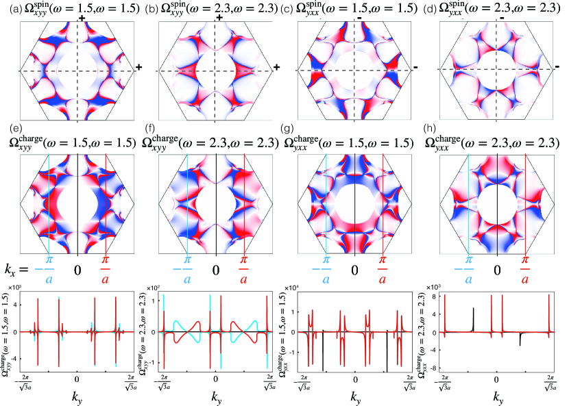
Next we discuss and of odd-number-layered NbSe2. Owing to the crystal symmetry, Neumann’s principle illustrates that the nonlinear optical charge Hall current is absent (generated) in even (odd)-number-layered NbSe2. Figures 6 (e) and (f) show the contour plots of for monolayer NbSe2 under light irradiation of and eV, respectively. In addition, below the each contour plot, the sliced at , and is shown. Here, blue, black and red lines indicate at , and , respectively. of has opposite sign to that of . Therefore, the -integration of over 1st BZ becomes identically zero, which is consistent with the result of Sec. III. Figures 6 (g) and (h) show the contour plots of in the 1st BZ under the light irradiation of and eV, respectively. Also, we show the sliced at , and . Because of has same sign to that of , it is clear that the -integration of over 1st BZ becomes finite, which reproduces the result of Fig. 2 (d). Thus, the nonlinear optical charge Hall current can be generated in -direction for monolayer NbSe2 by irradiating -polarized light.
Appendix D Energy band structures of bilayer NbSe2 with applied electric fields
Figures 7 (a), (b), (c) and (d) show the energy band structures and DOS of bilayer NbSe2 for several different electric fields. Here, red and blue lines show spin-up and spin-down states, respectively. Owing to the broken inversion symmetry in bilayer NbSe2 with applied electric fields, the energy band structures have larger spin splitting at the valence band edges in K and K′ points as same as the case of odd-number-layered NbSe2. In this paper, we provide the energy band structures with applied electric fields of , , and eV, respectively. Fermi levels are set to , , and eV for the applied electric fields of , , and eV, respectively.
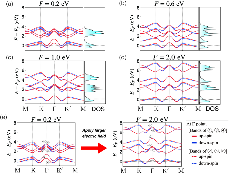
Figure 7 (e) indicates the energy bands can move by applying larger electric field in bilayer NbSe2. Here, the energy bands of solid lines (, and ) have positive parity between upper and lower layers of bilayer NbSe2, i.e., bonding molecular orbitals between the two layers. On the other hand, the energy bands of dashed lines (, and ) have negative parity between layers, i.e. anti-bonding configuration. With increase of electric field, the energy bands with negative (positive) parity shift up (down) to higher (lower) energy.
Appendix E Bilayer NbSe2 with each layer having a different Fermi energy
In this section, we consider the nonlinear optical spin and charge conductivities of bilayer NbSe2 with each layer having a different Fermi energy, i.e. decoupled bilayer NbSe2. Figure 8 (a) shows the energy band structure of decoupled bilayer NbSe2, where Fermi energy of the upper layer is and that of the lower layer is eV, respectively. Here, red and blue lines show spin-up and spin-down states, respectively. Since the upper and lower layers have the different Fermi energy, the energy band structure has spin splitting at K and K′ points as same as the case of odd-number-layered NbSe2.
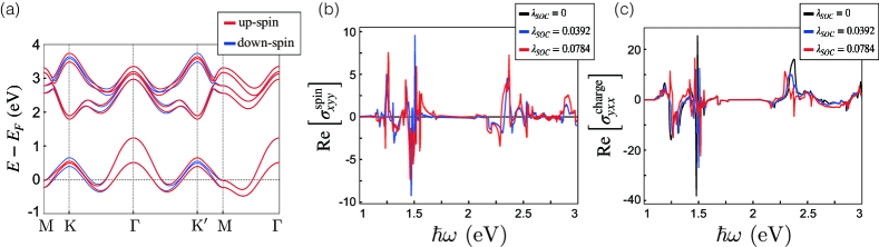
Figures 8 (b) and (c) show the real parts of nonlinear optical spin and charge Hall conductivities and of decoupled bilayer NbSe2, respectively. Here, both and are considerd as the case of SHG process and have Ising-type SOC parameter eV. Also, the cases for and eV are plotted for the comparison. Because of the Fermi energy imbalance between upper and lower layers, the nonlinear optical spin and charge Hall conductivities become finite even in the bilayer NbSe2, where several peaks appear below and above eV. The details of the imaginary parts of nonlinear optical spin and charge Hall conductivities are shown in Supplementary Material.
References
- Mak et al. (2010) K. F. Mak, C. Lee, J. Hone, J. Shan, and T. F. Heinz, “Atomically Thin : A New Direct-Gap Semiconductor,” Phys. Rev. Lett. 105, 136805 (2010).
- Splendiani et al. (2010) A. Splendiani, L. Sun, Y. Zhang, T. Li, J. Kim, C.-Y. Chim, G. Galli, and F. Wang, “Emerging Photoluminescence in Monolayer ,” Nano Lett. 10, 1271–1275 (2010).
- Tongay et al. (2012) S. Tongay, J. Zhou, C. Ataca, K. Lo, T. S. Matthews, J. Li, J. C. Grossman, and J. Wu, “Thermally Driven Crossover from Indirect toward Direct Bandgap in 2D Semiconductors: versus ,” Nano Lett. 12, 5576–5580 (2012).
- Gutiérrez et al. (2013) H. R. Gutiérrez, N. Perea-López, A. L. Elías, A. Berkdemir, B. Wang, R. Lv, F. López-Urías, V. H. Crespi, H. Terrones, and M. Terrones, “Extraordinary Room-Temperature Photoluminescence in Triangular Monolayers,” Nano Lett. 13, 3447–3454 (2013).
- Zhao et al. (2013) W. Zhao, Z. Ghorannevis, L. Chu, M. Toh, C. Kloc, P.-H. Tan, and G. Eda, “Evolution of Electronic Structure in Atomically Thin Sheets of and ,” ACS Nano 7, 791–797 (2013).
- Ciarrocchi et al. (2018) A. Ciarrocchi, A. Avsar, D. Ovchinnikov, and A. Kis, “Thickness-modulated metal-to-semiconductor transformation in a transition metal dichalcogenide,” Nat. Commun. 9, 919 (2018).
- Samadi et al. (2018) M. Samadi, N. Sarikhani, M. Zirak, H. Zhang, H.-L. Zhang, and A. Z. Moshfegh, “Group 6 transition metal dichalcogenide nanomaterials: synthesis, applications and future perspectives,” Nanoscale Horiz. 3, 90–204 (2018).
- Thakar and Lodha (2020) K. Thakar and S. Lodha, “Optoelectronic and photonic devices based on transition metal dichalcogenides,” Mater. Res. Express. 7, 014002 (2020).
- Wu et al. (2021) M. Wu, Y. Xiao, Y. Zeng, Y. Zhou, X. Zeng, L. Zhang, and W. Liao, “Synthesis of two-dimensional transition metal dichalcogenides for electronics and optoelectronics,” InfoMat 3, 362–396 (2021).
- Novoselov et al. (2005) K. S. Novoselov, D. Jiang, F. Schedin, T. J. Booth, V. V. Khotkevich, S. V. Morozov, and A. K. Geim, “Two-dimensional atomic crystals,” Proc. Natl. Acad. Sci. USA 102, 10451–10453 (2005).
- Desai et al. (2016) S. B. Desai, S. R. Madhvapathy, M. Amani, D. Kiriya, M. Hettick, M. Tosun, Y. Zhou, M. Dubey, J. W. Ager III, D. Chrzan, and A. Javey, “Gold-Mediated Exfoliation of Ultralarge Optoelectronically-Perfect Monolayers,” Adv. Mater. 28, 4053–4058 (2016).
- Lin et al. (2016) Z. Lin, A. McCreary, N. Briggs, S. Subramanian, K. Zhang, Y. Sun, X. Li, N. J. Borys, H. Yuan, S. K. Fullerton-Shirey, A. Chernikov, H. Zhao, S. McDonnell, A. M. Lindenberg, K. Xiao, B. J. LeRoy, M. Drndic, J. C. M. Hwang, J. Park, M. Chhowalla, R. E. Schaak, A. Javey, M. C. Hersam, J. Robinson, and M. Terrones, “2D materials advances: from large scale synthesis and controlled heterostructures to improved characterization techniques, defects and applications,” 2D Mater. 3, 042001 (2016).
- Yu et al. (2018) J. Yu, X. Hu, H. Li, X. Zhou, and T. Zhai, “Large-scale synthesis of 2D metal dichalcogenides,” J. Mater. Chem. C 6, 4627–4640 (2018).
- Wang et al. (2021) S. Wang, J.-K. Huang, M. Li, A. Azam, X. Zu, L. Qiao, J. Yang, and S. Li, “Growth of High-Quality Monolayer Transition Metal Dichalcogenide Nanocrystals by Chemical Vapor Deposition and Their Photoluminescence and Electrocatalytic Properties,” ACS Appl. Mater. Interfaces 13, 47962–47971 (2021).
- Zeng et al. (2012) H. Zeng, J. Dai, W. Yao, D. Xiao, and X. Cui, “Valley polarization in monolayers by optical pumping,” Nat. Nanotechnol. 7, 490–493 (2012).
- Mak et al. (2012) K. F. Mak, K. He, J. Shan, and T. F. Heinz, “Control of valley polarization in monolayer by optical helicity,” Nat. Nanotechnol. 7, 494–498 (2012).
- Cao et al. (2012) T. Cao, G. Wang, W. Han, H. Ye, C. Zhu, J. Shi, Q. Niu, P. Tan, E. Wang, B. Liu, and J. Feng, “Valley-selective circular dichroism of monolayer molybdenum disulphide,” Nat. Commun. 3, 887 (2012).
- Yu et al. (2015) H. Yu, X. Cui, X. Xu, and W. Yao, “Valley excitons in two-dimensional semiconductors,” Natl. Sci. Rev. 2, 57–70 (2015).
- Sinova et al. (2015) J. Sinova, S. O. Valenzuela, J. Wunderlich, C. H. Back, and T. Jungwirth, “Spin Hall effects,” Rev. Mod. Phys. 87, 1213–1260 (2015).
- Hai (2020) P. N. Hai, “Spin Hall Effect in Topological Insulators,” J. Magn. Soc. Jpn. 44, 137–144 (2020).
- Kato et al. (2004) Y. K. Kato, R. C. Myers, A. C. Gossard, and D. D. Awschalom, “Observation of the Spin Hall Effect in Semiconductors,” Science 306, 1910–1913 (2004).
- Wunderlich et al. (2005) J. Wunderlich, B. Kaestner, J. Sinova, and T. Jungwirth, “Experimental Observation of the Spin-Hall Effect in a Two-Dimensional Spin-Orbit Coupled Semiconductor System,” Phys. Rev. Lett. 94, 047204 (2005).
- Wen et al. (2019) X. Wen, Z. Gong, and D. Li, “Nonlinear optics of two-dimensional transition metal dichalcogenides,” InfoMat 1, 317–337 (2019).
- Lucas et al. (2021) L. Lucas, C. Aurea, Z. Tianyi, K. Ethan, B. Ismail, R. C. Bruno, K. Swastik, T. Mauricio, and M. M. Leandro, “Second- and third-order optical susceptibilities across excitons states in 2D monolayer transition metal dichalcogenides,” 2D Mater. 8, 035010 (2021).
- Taghizadeh and Pedersen (2019) A. Taghizadeh and T. G. Pedersen, “Nonlinear optical selection rules of excitons in monolayer transition metal dichalcogenides,” Phys. Rev. B 99, 235433 (2019).
- Trolle et al. (2014) M. L. Trolle, G. Seifert, and T. G. Pedersen, “Theory of excitonic second-harmonic generation in monolayer ,” Phys. Rev. B 89, 235410 (2014).
- Kumar et al. (2013) N. Kumar, S. Najmaei, Q. Cui, F. Ceballos, P. M. Ajayan, J. Lou, and H. Zhao, “Second harmonic microscopy of monolayer mos2,” Phys. Rev. B 87, 161403(R) (2013).
- Moss et al. (1987) D. J. Moss, J. E. Sipe, and H. M. van Driel, “Empirical tight-binding calculation of dispersion in the second-order nonlinear optical constant for zinc-blende crystals,” Phys. Rev. B 36, 9708–9721 (1987).
- Ghahramani et al. (1991) E. Ghahramani, D. J. Moss, and J. E. Sipe, “Full-band-structure calculation of second-harmonic generation in odd-period strained ()n/()n superlattices,” Phys. Rev. B 43, 8990–9002 (1991).
- Malard et al. (2013) Leandro M. Malard, Thonimar V. Alencar, Ana Paula M. Barboza, Kin Fai Mak, and Ana M. de Paula, “Observation of intense second harmonic generation from mos2 atomic crystals,” Phys. Rev. B 87, 201401(R) (2013).
- Seyler et al. (2015) K. L. Seyler, J. R. Schaibley, P. Gong, P. Rivera, A. M. Jones, S. Wu, J. Yan, D. G. Mandrus, W. Yao, and X. Xu, “Electrical control of second-harmonic generation in a monolayer transistor,” Nat. Nanotech. 10, 407–411 (2015).
- Rashkeev et al. (1998) S. N. Rashkeev, W. R. L. Lambrecht, and B. Segall, “Efficient method for the calculation of frequency-dependent second-order optical response in semiconductors,” Phys. Rev. B 57, 3905–3919 (1998).
- Rashkeev and Lambrecht (2001) S. N. Rashkeev and W. R. L. Lambrecht, “Second-harmonic generation of I-III- chalcopyrite semiconductors: Effects of chemical substitutions,” Phys. Rev. B 63, 165212 (2001).
- Sharma and Ambrosch-Draxl (2004) S. Sharma and C. Ambrosch-Draxl, “Second-Harmonic Optical Response from First Principles,” Phys. Scr. T109, 128 (2004).
- Leitsmann et al. (2005) R. Leitsmann, W. G. Schmidt, P. H. Hahn, and F. Bechstedt, “Second-harmonic polarizability including electron-hole attraction from band-structure theory,” Phys. Rev. B 71, 195209 (2005).
- Shen (1989) Y. R. Shen, “Surface properties probed by second-harmonic and sum-frequency generation,” Nature 337, 519–525 (1989).
- Shen (2020) Y. R. Shen, “Revisiting the basic theory of sum-frequency generation,” J. Chem. Phys. 153, 180901 (2020).
- Shultz et al. (2000) M. J. Shultz, C. Schnitzer, D. Simonelli, and S. Baldelli, “Sum frequency generation spectroscopy of the aqueous interface: Ionic and soluble molecular solutions,” Int. Rev. Phys. Chem. 19, 123–153 (2000).
- Richmond (2002) G. L. Richmond, “Molecular Bonding and Interactions at Aqueous Surfaces as Probed by Vibrational Sum Frequency Spectroscopy,” Chem. Rev. 102, 2693–2724 (2002).
- Shen and Ostroverkhov (2006) Y. R. Shen and V. Ostroverkhov, “Sum-Frequency Vibrational Spectroscopy on Water Interfaces: Polar Orientation of Water Molecules at Interfaces,” Chem. Rev. 106, 1140–1154 (2006).
- Gopalakrishnan et al. (2006) S. Gopalakrishnan, D. Liu, H. C. Allen, M. Kuo, and M. J. Shultz, “Vibrational Spectroscopic Studies of Aqueous Interfaces: Salts, Acids, Bases, and Nanodrops,” Chem. Rev. 106, 1155–1175 (2006).
- Ishiyama et al. (2014) T. Ishiyama, T. Imamura, and A. Morita, “Theoretical Studies of Structures and Vibrational Sum Frequency Generation Spectra at Aqueous Interfaces,” Chem. Rev. 114, 8447–8470 (2014).
- Tsang (1995) T. Y. F. Tsang, “Optical third-harmonic generation at interfaces,” Phys. Rev. A 52, 4116–4125 (1995).
- Squier et al. (1998) J. A. Squier, M. Müller, G. J. Brakenhoff, and K. R. Wilson, “Third harmonic generation microscopy,” Opt. Express 3, 315–324 (1998).
- Stock et al. (2020) C. Stock, K. Zlatanov, and T. Halfmann, “Third harmonic generation and microscopy, enhanced by a bias harmonic field,” Opt. Commun. 457, 124660 (2020).
- Dromey et al. (2006) B. Dromey, M. Zepf, A. Gopal, K. Lancaster, M. S. Wei, K. Krushelnick, M. Tatarakis, N. Vakakis, S. Moustaizis, R. Kodama, M. Tampo, C. Stoeckl, R. Clarke, H. Habara, D. Neely, S. Karsch, and P. Norreys, “High harmonic generation in the relativistic limit,” Nat. Phys. 2, 456–459 (2006).
- Winterfeldt et al. (2008) C. Winterfeldt, C. Spielmann, and G. Gerber, “Colloquium: Optimal control of high-harmonic generation,” Rev. Mod. Phys. 80, 117–140 (2008).
- Vampa et al. (2014) G. Vampa, C. R. McDonald, G. Orlando, D. D. Klug, P. B. Corkum, and T. Brabec, “Theoretical Analysis of High-Harmonic Generation in Solids,” Phys. Rev. Lett. 113, 073901 (2014).
- Pawlicki et al. (2009) M. Pawlicki, H. A. Collins, R. G. Denning, and H. L. Anderson, “Two-Photon Absorption and the Design of Two-Photon Dyes,” Angew. Chem. Int. Ed. 48, 3244–3266 (2009).
- Rumi and Perry (2010) M. Rumi and J. W. Perry, “Two-photon absorption: an overview of measurements and principles,” Adv. Opt. Photon. 2, 451–518 (2010).
- Wang et al. (2020) G. Wang, D. Bennett, C. (John) Zhang, C. Ó Coileáin, M. Liang, N. McEvoy, J. J. Wang, J. Wang, K. Wang, V. Nicolosi, and W. J. Blau, “Two-Photon Absorption in Monolayer enes,” Adv. Opt. Mater. 8, 1902021 (2020).
- Fryett et al. (2017) T. K. Fryett, A. Zhan, and A. Majumdar, “Phase-matched nonlinear optics via patterning layered materials,” Opt. Lett. 42, 3586–3589 (2017).
- He et al. (2021) J. He, D. Wei, and X. Wang, “Quasi-phase matching for a nonlinear photonic waveguide enabled by monolayer transition-metal dichalcogenide arrays,” J Korean Phys Soc 79, 380–385 (2021).
- Xiao et al. (2020) R.-C. Xiao, D.-F. Shao, Z.-Q. Zhang, and H. Jiang, “Two-Dimensional Metals for Piezoelectriclike Devices Based on Berry-Curvature Dipole,” Phys. Rev. Appl. 13, 044014 (2020).
- Zhou et al. (2020) B. T. Zhou, C.-P. Zhang, and K. T. Law, “Highly Tunable Nonlinear Hall Effects Induced by Spin-Orbit Couplings in Strained Polar Transition-Metal Dichalcogenides,” Phys. Rev. Appl. 13, 024053 (2020).
- Ma et al. (2019) Q. Ma, S.-Y. Xu, H. Shen, D. MacNeill, V. Fatemi, T.-R. Chang, A. M. M. Valdivia, S. Wu, Z. Du, C.-H. Hsu, S. Fang, Q. D. Gibson, K. Watanabe, T. Taniguchi, R. J. Cava, E. Kaxiras, H.-Z. Lu, H. Lin, L. Fu, N. Gedik, and P. Jarillo-Herrero, “Observation of the nonlinear Hall effect under time-reversal-symmetric conditions,” Nature 565, 337+ (2019).
- Sodemann and Fu (2015) I. Sodemann and L. Fu, “Quantum Nonlinear Hall Effect Induced by Berry Curvature Dipole in Time-Reversal Invariant Materials,” Phys. Rev. Lett. 115, 216806 (2015).
- Wilson et al. (2001) J. A. Wilson, F. J. Di Salvo, and S. Mahajan, “Charge-density waves and superlattices in the metallic layered transition metal dichalcogenides,” Adv. Phys. 50, 1171–1248 (2001).
- Kim and Son (2017) S. Kim and Y.-W. Son, “Quasiparticle energy bands and Fermi surfaces of monolayer ,” Phys. Rev. B 96, 155439 (2017).
- He et al. (2018) W.-Y. He, B. T. Zhou, J. J. He, N. F. Q. Yuan, T. Zhang, and K. T. Law, “Magnetic field driven nodal topological superconductivity in monolayer transition metal dichalcogenides,” Commun. Phys. 1, 40 (2018).
- Xi et al. (2016) X. Xi, Z. Wang, W. Zhao, J.-H. Park, K. T. Law, H. Berger, L. Forró, J. Shan, and K. F. Mak, “Ising pairing in superconducting atomic layers,” Nat. Phys. 12, 139–143 (2016).
- Sohn et al. (2018a) E. Sohn, X. Xi, W.-Y. He, S. Jiang, Z. Wang, K. Kang, J.-H. Park, H. Berger, L. Forró, K. T. Law, J. Shan, and K. F. Mak, “An unusual continuous paramagnetic-limited superconducting phase transition in 2D ,” Nat. Mater. 17, 504–508 (2018a).
- Anikin et al. (2020) A. Anikin, R. D. Schaller, G. P. Wiederrecht, E. R. Margine, I. I. Mazin, and G. Karapetrov, “Ultrafast dynamics in the high-symmetry and in the charge density wave phase of 2-,” Phys. Rev. B 102, 205139 (2020).
- Lian et al. (2017) C.-S. Lian, C. Si, J. Wu, and W. Duan, “First-principles study of -intercalated bilayer : Suppressed charge-density wave and strain-enhanced superconductivity,” Phys. Rev. B 96, 235426 (2017).
- Lu et al. (2015) J. M. Lu, O. Zheliuk, I. Leermakers, N. F. Q. Yuan, U. Zeitler, K. T. Law, and J. T. Ye, “Evidence for two-dimensional Ising superconductivity in gated ,” Science 350, 1353–1357 (2015).
- Saito et al. (2016) Y. Saito, Y. Nakamura, M. S. Bahramy, Y. Kohama, J. Ye, Y. Kasahara, Y. Nakagawa, M. Onga, M. Tokunaga, T. Nojima, Y. Yanase, and Y. Iwasa, “Superconductivity protected by spin–valley locking in ion-gated ,” Nat. Phys. 12, 144–149 (2016).
- Zhou et al. (2016) B. T. Zhou, N. F. Q. Yuan, H.-L. Jiang, and K. T. Law, “Ising superconductivity and Majorana fermions in transition-metal dichalcogenides,” Phys. Rev. B 93, 180501(R) (2016).
- Bawden et al. (2016) L. Bawden, S. P. Cooil, F. Mazzola, J. M. Riley, L. J. Collins-McIntyre, V. Sunko, K. W. B. Hunvik, M. Leandersson, C. M. Polley, T. Balasubramanian, T. K. Kim, M. Hoesch, J. W. Wells, G. Balakrishnan, M. S. Bahramy, and P. D. C. King, “Spin–valley locking in the normal state of a transition-metal dichalcogenide superconductor,” Nat. Commun. 7, 11711 (2016).
- Habara and Wakabayashi (2021) R. Habara and K. Wakabayashi, “Optically induced spin current in monolayer ,” Phys. Rev. B 103, L161410 (2021).
- (70) See Supplementary Material at [URL will be inserted by publisher] for nonlinear optical Hall conductivity of SFG process. Temperature effect and behavior of TMDC semiconductor on nonlinear optical spin and charge Hall currents are also presented.
- Liu et al. (2013) G.-B. Liu, W.-Y. Shan, Y. Yao, W. Yao, and D. Xiao, “Three-band tight-binding model for monolayers of group-VIB transition metal dichalcogenides,” Phys. Rev. B 88, 085433 (2013).
- Sohn et al. (2018b) E. Sohn, X. Xi, W.-Y. He, S. Jiang, Z. Wang, K. Kang, J.-H. Park, H. Berger, L. Forro, K. T. Law, J. Shan, and K. F. Mak, “An unusual continuous paramagnetic-limited superconducting phase transition in 2D ,” Nat. Mater. 17, 504–508 (2018b).
- Kang and Choi (2010) N. L. Kang and S. D. Choi, “Derivation of nonlinear optical conductivity by using a reduction identity and a state-dependent projection method,” J. Phys. A Math. Theor. 43, 165203 (2010).
- Lee et al. (2002) H. J. Lee, N. L. Kang, J. Y. Sug, and S. D. Choi, “Calculation of the nonlinear optical conductivity by a quantum-statistical method,” Phys. Rev. B 65, 195113 (2002).
- Kang and Choi (2012) N. L. Kang and S. D. Choi, “Derivation of second-order nonlinear optical conductivity by the projection-diagram method,” AIP Adv. 2, 012161 (2012).
- Kang et al. (2013) N. L. Kang, S.-S. Lee, and S. D. Choi, “Projection-reduction method applied to deriving non-linear optical conductivity for an electron-impurity system,” AIP Adv. 3, 072104 (2013).
- Aversa and Sipe (1995) C. Aversa and J. E. Sipe, “Nonlinear optical susceptibilities of semiconductors: Results with a length-gauge analysis,” Phys. Rev. B 52, 14636–14645 (1995).
- Sipe and Ghahramani (1993) J. E. Sipe and E. Ghahramani, “Nonlinear optical response of semiconductors in the independent-particle approximation,” Phys. Rev. B 48, 11705–11722 (1993).
- Lu et al. (2011) Q. Y. Lu, N. Bandyopadhyay, S. Slivken, Y. Bai, and M. Razeghi, “Room temperature single-mode terahertz sources based on intracavity difference-frequency generation in quantum cascade lasers,” Appl. Phys. Lett. 99, 131106 (2011).
- Axel et al. (2012) R. Axel, G. Alessio, H. Ingmar, E. F. Martin, S. E. E. Kjeld, and M. Marco, “Widely-tunable mid-infrared frequency comb source based on difference frequency generation,” Opt. Lett. 37, 2232–2234 (2012).
- Passos et al. (2021) D. J. Passos, G. B. Ventura, J. M. B. Lopes dos Santos, and J. M. Viana Parente Lopes, “Nonlinear optical conductivity of a two-band crystal I,” J. Phys. Condens. Matter 33, 465701 (2021).
- Zeng et al. (2021) C. Zeng, S. Nandy, and S. Tewari, “Nonlinear transport in Weyl semimetals induced by Berry curvature dipole,” Phys. Rev. B 103, 245119 (2021).
- Kim and Son (2021) S. Kim and Y.-W. Son, “Dichotomy of saddle points in energy bands of monolayer ,” Phys. Rev. B 104, 045426 (2021).