©2021 IEEE. Personal use of this material is permitted. Permission from IEEE must be obtained for all other uses, in any current or future media, including reprinting/republishing this material for advertising or promotional purposes, creating new collective works, for resale or redistribution to servers or lists, or reuse of any copyrighted component of this work in other works.
This work has been accepted at the 2022 30th IEEE International Symposium on Field-Programmable Custom Computing Machines (FCCM) and will appear in the proceedings and on the IEEE website on/around May 15, 2022.
CoMeFa: Compute-in-Memory Blocks for FPGAs
Abstract
Block RAMs (BRAMs) are the storage houses of FPGAs, providing extensive on-chip memory bandwidth to the compute units implemented using Logic Blocks (LBs) and Digital Signal Processing (DSP) slices. We propose modifying BRAMs to convert them to CoMeFa (Compute-In-Memory Blocks for FPGAs) RAMs. These RAMs provide highly-parallel compute-in-memory by combining computation and storage capabilities in one block. CoMeFa RAMs utilize the true dual port nature of FPGA BRAMs and contain multiple programmable single-bit bit-serial processing elements. CoMeFa RAMs can be used to compute in any precision, which is extremely important for evolving applications like Deep Learning. Adding CoMeFa RAMs to FPGAs significantly increases their compute density. We explore and propose two architectures of these RAMs: CoMeFa-D (optimized for delay) and CoMeFa-A (optimized for area). Compared to existing proposals, CoMeFa RAMs do not require changing the underlying SRAM technology like simultaneously activating multiple rows on the same port, and are practical to implement. CoMeFa RAMs are versatile blocks that find applications in numerous diverse parallel applications like Deep Learning, signal processing, databases, etc. By augmenting an Intel Arria-10-like FPGA with CoMeFa-D (CoMeFa-A) RAMs at the cost of 3.8% (1.2%) area, and with algorithmic improvements and efficient mapping, we observe a geomean speedup of 2.5x (1.8x), across several representative benchmarks. Replacing all or some BRAMs with CoMeFa RAMs in FPGAs can make them better accelerators of modern compute-intensive workloads.
I Introduction
FPGAs are being used to accelerate workloads ranging from internet search, to baseband processing, to the ubiquitous Deep Learning (DL). FPGAs contain fine-grained programmable logic blocks (LBs), fixed-function math units (DSP slices), and distributed Block Random Access Memory (BRAM) structures that are connected via a highly configurable interconnection fabric. BRAMs play a vital role by storing operands and results on-chip, feeding the compute units with data at a very high bandwidth.
The current usage paradigms of BRAMs, LBs and DSPs pose limitations to the acceleration that can be achieved using FPGAs. In many large FPGAs deployed in cloud applications, hundreds of MBytes of data can be stored on-chip in BRAMs, enabling fully-data-resident acceleration. However, in applications where on-chip storage requirements are low (eg. where data is streamed to the FPGA), BRAMs may be left idle. Additionally, BRAMs on FPGAs support a limited set of heights and widths. This can limit the bandwidth available to the compute units because the data needs to be read out from pins of the BRAM. The separation of compute units (LBs and DSPs) from storage units (BRAMs) implies data movement using the routing/interconnect to feed the compute units with input data and to store the outputs back to the storage units. This stresses the routing resources significantly and leads to increased power consumption.
FPGAs provide the ability to develop hardware for different precisions. This is especially important for DL applications, because the precision requirements change rapidly. DSP slices, however, support a limited set of precisions. Designers end up implementing low precision math units on LBs instead of DSPs, reducing the number of LBs available for other purposes and leaving DSPs unused.
In this paper, we solve the limitations mentioned above by proposing to convert BRAMs on an FPGA to CoMeFa RAMs. A CoMeFa RAM block enables computation within the RAM array, without transferring the data in or out of it. One-bit bit-serial programmable processing elements are added at the output of the sense amplifiers. This transforms the BRAM into a parallel SIMD (Single Instruction Multiple Data) computation unit. The availability of true dual port mode in FPGA BRAMs [1][2] is exploited to read operands.
Computation in any precision can be easily performed in CoMeFa RAMs without any explicit hardware because it uses bit-serial compute [3]. CoMeFa RAMs reduce the dependence on routing/interconnect and hence increases the routability of the FPGA. Data movement is reduced because the computation is done in the RAM itself, thereby saving power. Since the data is not moved in/out of the RAM block, pin limitations do not restrict the available bandwidth. Instead, the internal physical geometry of the RAM, which is typically higher than port width, governs the effective bandwidth. The compute throughput of the FPGA is increased significantly owing to the massive parallelism that is unlocked because of the existence of numerous RAM blocks on an FPGA.
CoMeFa RAMs are not replacements of DSPs or LBs, but can work together and complement them. In some ways, CoMeFa RAMs can be thought of blocks that fuse together Logic Blocks and BRAMs. They provide a more structured way of computation compared to Logic Blocks, along with storage capability of BRAMs. They are more flexible than DSP Slices owing to their precision agnosticism. They can be used in diverse parallel applications like DL, signal and image processing, databases, compression, encoding, decoding, etc. Because of the bit-serial nature of the compute, CoMeFa RAMs are particularly suited for throughput-oriented latency-tolerant workloads. Workloads with low-precision compute and bit-wise operations are also well accelerated using CoMeFa RAMs. Note that CoMeFa RAMs can still store data and operate identically like a BRAM. Unused BRAMs can be used as CoMeFa RAMs increasing the available compute throughput and hence, achieving faster acceleration.
II Background
II-A Bit Serial Computing
Bit serial computing is commonly used for digital signal processing and has been used on FPGAs as well [4] [5]. The main idea is to process one bit of multiple data elements every cycle. This is different from bit-parallel computing, in which multiple bits of one data element are processed every cycle. As an example, a conventional bit-parallel processor will take 128 steps to perform element-wise sum of two arrays with 128 16-bit elements. A bit-serial processor with 128 processing elements would complete the operation in 16 steps as it processes the arrays bit-by-bit instead of element-by-element. Since the number of elements in arrays is typically greater than the bit-precision of elements, bit-serial computing can provide much higher throughput compared to bit-parallel computing, albeit at higher latency for each result.
II-B Compute-In-Memory
Compute-In-Memory or Processing-In-Memory (PIM) [6] is the paradigm of bringing computation closer to the data, instead of moving data to distant compute units. Many accelerators using PIM have been proposed and deployed: ReRAM based [7] [8] [9], DRAM based [10] [11] [12], and SRAM based [13] [14] [15] [16]. Computational RAM (or C-RAM) [17] is an architecture where a row of processing elements (PEs) is added to a memory (DRAM or SRAM) to convert it into a SIMD processor. Jeloka et. al. [18] created a logic-in-memory SRAM prototype where multiple word lines are activated simultaneously and the shared bit-lines can be sensed, effectively performing logical AND and NOR operations on the data stored in the activated rows. In Neural Cache, Eckert et. al. apply this technology to DL applications [3], adding processing elements to the sense amplifiers and deploy bit-serial compute to perform DL operations. Wang et. al. proposed integrating the technology from Neural Cache into FPGA BRAMs to create Compute Capable BRAMs (CCB) [19]. The complexity associated with the reduction in voltage required to ensure robustness when activating multiple wordlines makes this architecture not very practical.
III Proposed Architecture: CoMeFa RAMs
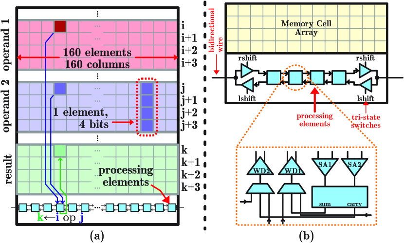
In this section, we describe the proposed changes to BRAMs to convert them to CoMeFa RAMs. We consider a BRAM size of 20 Kilobits as in the modern Intel FPGAs, with support for single port, simple dual port and true dual port modes, with the 512x40 being the shallowest and widest configuration. This BRAM has a physical geometry of 128 rows x 160 columns with a column multiplexing factor of 4 [20] [21].
III-A Overview
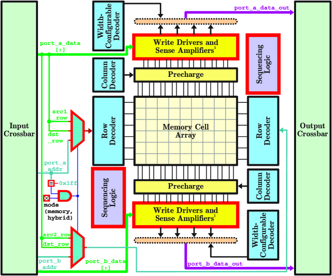
Figure 1 shows a top-level diagram of an FPGA BRAM, with blocks modified/added for CoMeFa RAM shown with a red outline. We explore two architectures at the ends of the area-delay design space (evaluating other candidates in this space is left as future work).
CoMeFa-D: In this architecture, we add additional sense amplifiers and write drivers to enable reading and writing a row in all columns (bitline pairs) together. A processing element (PE) is added below each column. This is similar to the architecture used in [3], [23] and [19]. During physical design/implementation, PEs should be laid out so that they pitch-match with the SRAM cells (and sense amplifiers and write drivers) for a bitline pair (BL and BLB). There are 160 sense amplifiers and write drivers per port, and 160 PEs. This provides a parallelism 160 operations done in 1 clock cycle (slightly longer than the baseline BRAM’s clock period) at cost of high area overhead. This architecture is more practical than CCB because multiple wordlines are not accessed simultaneously on a port and voltage reduction is not required for robustness.
CoMeFa-A: In this architecture, the number of sense amplifiers and write drivers stays the same as the baseline. A different PE is added below each multiplexed column. An optimization technique called sense amp cycling [24] is employed to sequentially sense column multiplexed bits in an extended clock cycle. There are 40 sense amplifiers and write drivers per port, and 40 PEs in the RAM. This provides a parallelism 160 operations done in 1 extended clock cycle, thereby trading off delay for area. This architecture has the highest practicality among CCB and CoMeFa variations.
The PEs use wires from the peripheral circuitry of both ports of the RAM. Sequencing logic that sequences the events of the read/write operations (wordline activation, precharge, sense amp enable, etc) in the memory is modified. This is done to support doing both read and write in one cycle. Some additional logic (comparator, configuration bit, multiplexers in front of row decoders) are also added, and will be explained in detail in this section.
III-B Modes and Phases
As shown in Figure 1, a new configuration SRAM cell is added which decides the mode of operation of a CoMeFa RAM block. A CoMeFa RAM can operate in two modes:
-
•
Memory Mode: In this mode, CoMeFa RAM behaves as a conventional BRAM with no change in functionality. In this mode, the designer can flexibly configure the number of ports and the width/depth of the BRAM.
-
•
Hybrid Mode: If this mode is enabled at configuration time, the CoMeFa RAM can be used for computation as well as storage. In this mode, the RAM is automatically configured to its maximum width (512x40) to maximize the read/write throughput for populating the memory array with input data and reading the results. A special address (0x1FF) is reserved. A comparator is added to Port A’s address signal to check for this address (Figure 1). Data written to this address is treated as an instruction. Accessing other addresses is done normally; used for storing operands and reading results.
A clock cycle during computation has 3 phases. In the first phase, two rows containing operand bits are read by activating the corresponding word lines, one from each port. In the second phase, the logic gates in the PE compute the result. In the third phase, the result is stored back by activating a wordline. This leads to a longer clock period, compared to typical BRAM.
III-C Processing element
Fig 2 shows the structure of PE added to each column of the memory in CoMeFa-D. On the read path, A and B are the bits of the two operands read from the memory at sense amplifiers SA1 and SA2 of the two ports. Multiplexer TR evaluates a logical function of A and B, depending on the inputs TR0, TR1, TR2, TR3 (truth table) that come from the instruction. If a 2-bit addition is required, the truth table bits will correspond to that of an XOR gate. The output of TR goes through another XOR gate (X) to generate the addition of the input bits including the previous cycle’s carry (S). Gates to generate the carry (CGEN) are also present. The carry is stored in the carry latch (C) and can be used in the following cycle’s computation. If an addition operation is not required, the carry latch is reset with C_RST=1, which enables X to pass the output of TR transparently to the S wire. C_EN=0 disables the latch so it keeps the old value. The read outputs A and B are also sent to d_out1 and d_out2, which is the normal read path.
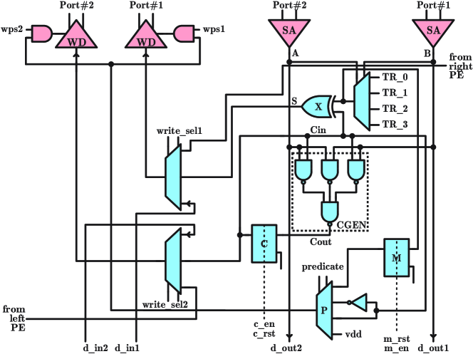
On the write path, 3-input multiplexers W1 and W2 are added before the write drivers of the two ports. These multiplexers determine the sources for the write operation. W1 can select between the S, the input data port d_in1 (normal write operation) and the value read from the right neighboring PE (used during left shift operation). W2 can select between the carry, the input data port d_in2 (normal write operation) and the value read from the left neighboring PE (used during the right shift operation). The mux select signals for W1 and W2 come from the instruction.
The output of multiplexer TR is also stored in a special latch called M and is called mask. Predication logic allows enabling/disabling the write drivers (WD1 and WD2). For this, a multiplexer (P) is added to select the signal that will enable/disable the write drivers. The mask, carry, not-carry and VDD (logic 1) can be selected. This helps CoMeFa RAMs mask writing the results based on various conditions, like the value of the mask or the carry bit, to support multiplications and floating point operations. The wps* signals decide which port’s write path is activated for a given cycle.
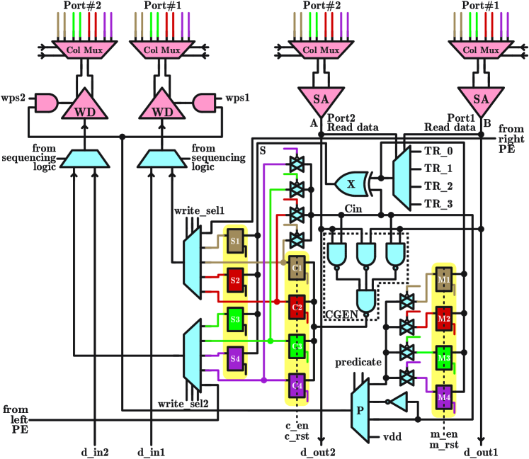
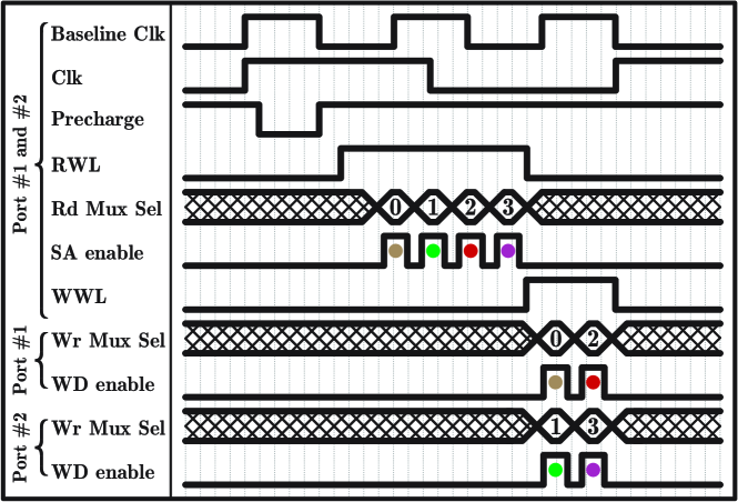
Fig 3 shows the structure of PE added to each multiplexed column of the memory in CoMeFa-A. All the labels have the same meaning as the PE described above. The number of C and M latches changes to 4, and there are 4 additional latches for S. On each port, 4 column-multiplexed bits are read and two results are written back in an extended clock cycle. In the read phase of the cycle, the brown bitline pairs from each port are sensed first. The resulting S bit is stored in latch S1, carry bit C is stored in the latch C1, and mask bit M is stored in latch M1. This is repeated for red, green, and purple bitline pairs successively. All Sn, Cn and Mn latches get updated in this process. Then, in the write phase of the cycle, results for the brown and red bitlines are written using the write drivers of the two ports, followed by the green and purple ones. This is shown in Fig 4. Clocks in the PE are driven by signals derived from the sense amplifier enable pulses. The paths in the PE do not add any additional delay to the extended clock from sense amp cycling.
III-D Instructions
An instruction is 40-bits and is only required to be written to Port A’s data bus. The format is shown in Figure 5. The field names in the instruction are self-explanatory. They directly drive the corresponding signals in the PE (e.g. predicate bits are applied to the select lines of the multiplexer P). The src1_row, src2_row and dst_row bits are used for activating first operand row on Port A, second operand row on Port B and the row at which results will be stored, respectively. These addresses are fed to the appropriate row decoders at the right time in the clock cycle by the sequencing logic in the CoMeFa RAM using the multiplexers shown in Figure 1. A designer can choose to generate instructions by finite state machines (FSM) implemented in soft logic, or store them in another BRAM on-chip and apply them to a CoMeFa RAM. Multiple CoMeFa RAMs can share instruction generation logic to amortize its cost.

III-E Operation
All computation is done in a bit-wise manner, using transposed data layout. Figure 6 (a) shows how elements are stored, read, computed on (based on the truth_table bits in the instruction) and the result stored back, row-by-row. For performing addition operation, in each cycle, the PE computes the sum, stores the carry for the next cycle computation, and writes back the sum bit to the result row. Then the next bit position is processed in the next cycle, using the stored carry. The final carry is stored into a row using an extra cycle. Thus, the addition for -bit operands takes cycles. Multiplication is based on iterative addition of partial results. In each iteration, one bit of the first operand is loaded as into the mask latch, and the second operand’s bits are added to the partial sum only if the mask is 1. Multiplication of -bit operands takes cycles. The addition and multiplication algorithm mentioned above, and also in-RAM reduction algorithm are detailed in [3].
III-F RAM-to-RAM chaining
CoMeFa RAMs provide the capability of performing left-shift and right-shift operations efficiently. Shifts are single operand operations. For a left (right) shift operation, the source operand row is read into the PEs, each PE’s W1 (W2) mux is configured to select the bit read from the right (left) neighboring PE, and that bit is written into the destination row. For CoMeFa-A, shifting values from a bitline pair to another bitline pair within the same column multiplexer is also supported. Direct connections are provided between neighboring CoMeFa RAMs in a column to allow for shifting data between the corner PEs in each CoMeFa RAM. These connections can provide a much easier way to perform inter-CoMeFa RAM communication and obtain even more parallelism. Figure 6 (b) shows these direct connections between CoMeFa RAMs along with the details of the shift operation support inside each PE.
III-G Variable precision support
Hardware in CoMeFa RAM PEs is not specific to any numerical precision. A different sequence of instructions is all that’s required to compute in a different precision. The sequences for fixed-point addition and multiplication were explained in Section III-E. CoMeFa RAMs can natively support floating point precisions as well, as opposed to CCB [19]. We adapt the floating point algorithms for addition and multiplication from FloatPIM [9]. The CoMeFa RAM PE can perform all the steps in the sequences because: (1) carry and not-carry are used in the predication logic, (2) mask is populated from the output of the programmable multiplexer TR instead of just A or B, and (3) operations like XOR can be performed easily using TR and the truth_table fields in the instruction. The approximate number of cycles consumed for floating point multiplication and addition are and , where = number of mantissa bits and = number of exponent bits.
III-H Data loading and unloading
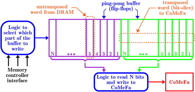
As mentioned in Section III-E, data has to be stored in a transposed layout in CoMeFa RAMs for computation. We design a swizzle module (implemented in soft logic) that can be used to read data from DRAM, transpose it and write it a CoMeFa RAM on-the-fly. The architecture of the swizzle logic is shown in Figure 7. The swizzle module employs a ping-pong buffer FIFO. Untransposed data read from DRAM is written in-order into the ping part of the FIFO (depth = 40 elements). When the ping part is full, a transposed word (a bit slice from 40 elements) can be read and written into consecutive bitlines on the same wordline in a CoMeFa RAM, and new data from DRAM is written into the pong part. In a similar fashion, transposed data can be read from CoMeFa RAMs and stored into DRAM in untransposed form using swizzle logic.
III-I One Operand Outside RAM (OOOR) operations
In Section III-E, two operands were stored inside the RAM. However, in many cases, an optimization can be applied - one of the operand can be outside the RAM. E.g, multiplying an array of numbers (stored in the RAM) with a scalar operand (outside the RAM). We call these OOOR ops. This method saves space inside the RAM. Without OOOR, in the multiplication example, we would need to replicate the scalar operand in each column. It allows easy inspection of outside operand’s bits, thereby enabling efficient algorithms. For example, in the normal shift-and-add based multiplication explained in [3], if a bit in the scalar operand is 0, cycles are still consumed, which can be avoided by using OOOR. In the average case, half of the bits will be 0 and therefore, the number of cycles can be reduced by 50%. Efficient algorithms like booth multiplication can also be deployed. We apply OOOR to dot-product where one of the vector’s elements are common to all columns. Looking at corresponding pairs of bits across the operands outside the RAM and adding partial sums inside the RAM based on their values enabled a 2x speedup compared to the naive algorithm. Overall, OOOR operations make the processing elements more powerful and capable by enabling expressing 2 (or 3) operand operations as 1 (or 2) operand operations for the PE.
IV Evaluation
IV-A Tools and Methods Used
The Verilog-to-Routing (VTR) tool flow [25] is used to evaluate and compare FPGA architectures. To obtain the area and delay values for the various components of the FPGA, including CoMeFa RAMs, we use COFFE [26]. COFFE based SPICE simulations use 22nm libraries from Predictive Technology Model [27]. We also perform SPICE simulations using FreePDK45 [28] to get more confidence that the read+compute+write operation of CoMeFa RAMs works and to validate the numbers obtained from COFFE.
We use an analytical model to estimate the energy consumption. We add transistor energy and wire energy. For transistor energy, we use an activity factor of 0.1 and calculate the energy based on the number of transistors in each block (obtained from the area consumed by the block from VTR). For wire energy, we use wire energy numbers (fJ/mm) from [29], scale them to 22nm technology node using [30] and multiply that with the total routing wirelength from VTR.
IV-B Baseline vs. Proposed Architectures
We use an Intel Arria 10-like FPGA architecture as baseline with the same resources as Aria 10 GX900 [31] (Table I. Arria 10 FPGAs [2] use a technology node (20nm) similar to our setup (22nm). Arria 10 GX900 has 96 transceiver channels that support upto 17.4 Gbps [32]. We assume that a 4-port full-width soft HMC (Hybrid Memory Cube) controller [33] is implemented on the FPGA to provide a DRAM bandwidth of 2048 bits/clock. Resources consumed by the controller are not used to map the applications to the FPGA.
We use the VTR FPGA architecture used in [34], modified for our requirements, to make a baseline architecture file. We run COFFE simulations on an Arria-10 like DSP to indentify its delay and area. We get delay and areas of a 20 Kilobit BRAM from COFFE (by interpolating between 16K and 32K). We scale these results based on the DSP and BRAM delays specified in [35]. The DSP slice works at 630 MHz in fixed-point mode and 550 MHz in floating-point mode. The BRAM works at 735 MHz in single port, simple dual port and true dual port modes. The proposed architecture files (CoMeFa-D and CoMeFa-A) differ from the baseline in having CoMeFa RAMs instead of normal BRAMs.
(Intel Arria 10 GX 900 like)
| Resource | Count | Percentage Area |
|---|---|---|
| Logic Blocks | 33962 | 66 |
| DSP Slices | 2423 | 18 |
| Block RAMs | 1518 | 15 |
| DRAM bandwidth | 2048 bits/clock | |
| Channel width | 300 | |
IV-C Benchmarks
| Benchmark | Domain | Scenario Created | Storage | Precision |
| GEMV | DL | CB | DRAM | 8-bit |
| FIR filter | DSP | CB | DRAM | 16-bit |
| Eltwise mult | DL | DBB | DRAM | HFP8 |
| Bulk bitwise-Search | Databases | OMB | BRAM | 16-bit |
| Bulk bitwise-RAID | Data Center | OMB | BRAM | 20-bit |
| Reduction | DL | OMB | BRAM | Multiple |
We create Verilog designs for several diverse applications to use as benchmarks (Table II). We manually map the applications to CoMeFa RAMs and instantiate the CoMeFa RAM block in Verilog, which is mapped to CoMeFa RAMs in the FPGA architecture provided to VTR. During functional verification, a simulation model of CoMeFa RAM is used. We create different scenarios (compute bound, DRAM bandwidth bound and on-chip memory bound) in these applications.
General Matrix Vector Multiplication (GEMV): GEMV is a fundamental operation in DL applications. It is used in CNNs, LSTM cells and in MLPs. We consider GEMV workloads from DeepBench benchmarks [36] - LSTM,h=512,t=50 and GRU,h=512,t=1. 8-bit integer precision with 27-bit accumulation is used. On the baseline FPGA, compute units are implemented using efficient chaining of DSPs. On the proposed FPGA, compute units based on CoMeFa RAMs are additionally deployed, because many RAM blocks are available after mapping the baseline design on the proposed FPGA. Efficient OOOR-based dot product algorithm is used. Partial sums are read out from the CoMeFa blocks and accumulated using a pipelined bit-serial tree [4]. No online data transpose is required - the weight matrix is transposed offline and pinned into CoMeFa RAM blocks; the vector is streamed and does not need to be transposed because it is outside the RAM. Since both DSP based and CoMeFa based compute units are used, reduction in data movement is not expected.
Finite Impulse Response (FIR) Filter: FIR filters are a common DSP application. We consider an FIR filter with 128 taps (similar results were observed for 256 taps; not shown here because of space constraints). Input operands are streamed onto the FPGA through the DRAM interface. The baseline FPGA uses an efficient implementation of FIR filter using systolic DSP chaining [37]. The proposed FPGA uses CoMeFa RAMs for computation along with DSP chains. Logic blocks were used for control logic. Operands are transposed on-the-fly and loaded into multiple CoMeFa RAMs in parallel. While some CoMeFa RAMs are computing, other CoMeFa RAMs are loaded in a pipelined manner to improve parallelism. When a CoMeFa RAM finishes computing, its results are unloaded and sent to DRAM, and the process starts again until all inputs are processed. We call this the Load-Compute-Unload (LCU) pipeline. In this application, the CoMeFa RAM-to-CoMeFa RAM chaining (Section III-F) feature is used to share inputs between neighboring blocks.
Elementwise multiplication: Elementwise multiplications are commonly used in DL, for example, in normalization layers and Winograd based convolution layers. We consider an application involving elementwise multiplication of two arrays of 100K elements. Floating point data with precision of HFP8 [38] is used. We showcase here that CoMeFa RAMs are adaptable to any custom precision. The operands are read from DRAM and the results are written to DRAM. This is a DRAM bandwidth bound application because of low arithmetic intensity. We observed that the number of LBs used (16748) was significantly higher than in the baseline FPGA (649). To saturate the DRAM bandwidth available on the chip, many swizzle logic instances are required. To reduce this impact, we plan to explore hardening swizzle logic or adding Transpose Memory Units [3].
Bulk bitwise operations: Bulk bitwise operations (like AND, OR, XOR, etc) are commonly used in databases, encryption, DNA sequence alignment, etc. CoMeFa RAMs are very efficient at these massively parallel operations because of the presence of mux-based fully configurable PEs. The operands are assumed to be available in BRAMs in the right layout. The speedup seen in these applications attributed to the effective increase in on-chip memory bandwidth because 160 bits can be operated upon in 1 cycle in a CoMeFa RAM, compared to only 40 bits from a BRAM in the baseline FPGA. We consider two applications in this category.
Database search: In this application, records matching a key are searched. If a record matches the key, it is replaced with a special marker data (like constant 0). Each operand is bitwise XOR’ed with the key. Bitwise OR reduction is performed on the result. And then a bitwise ANDing operation is performed to zero-out the operands that match the key. 256 RAM blocks are used to store operands. In CoMeFa RAM, 7 data elements are stored in each column and temporary results consume 16 rows. The key is outside the RAM.
RAID data recovery: In RAID (Redundancy Array of Independent Disks) arrays, parity protection is used. If a drive in an array fails, the remaining data on other drives is combined with the parity data (using XOR) to reconstruct the missing data. These numerous parallel XOR operations with the parity data can be accelerated using an FPGA. Instead of storing operands in a transposed format (bits of one operand in multiple rows), we use an un-transposed data layout where we store bits of one operand in one row and bits of the second operand are in another row. This works for logical operations like bitwise XOR where there is no dependency/communication between consecutive bits, and avoids the overhead of transposing data.
Reduction: Reduction (or accumulation) is heavily used in DL and DSP applications. We design this application to create a scenario of an on-chip memory bandwidth limited application. Data is available in transposed format (computed in RAM by a prior kernel for example). The precision is varied from 4-bit to 20-bit (accumulator size = 32-bit). In the baseline, operands stored in BRAMs are read and successively accumulated using a pipelined adder tree (in LBs). On the proposed FPGA, CoMeFa RAMs store the operands. The reduction algorithm from [3] is used to reduce the elements to 40 partial sums (1 partial sum in each column of the RAM). These intermediate results from multiple CoMeFa RAMs are then read out and accumulated using a pipelined bit-serial adder [4] to obtain the result. A significantly smaller number of LBs (~2x-3.5x) is required on the proposed FPGA.
IV-D Implementation Details
Area: Table III shows the area breakdown of both architectures of CoMeFa RAM. For CoMeFa-D, the area overhead is 1546.78 . This represents an increase of 25.4% in the BRAM tile area compared to the baseline. This overhead is mainly attributed to the addition of 160 PEs and the additional 120 sense amplifiers and write drivers. With BRAMs occupying 15% of the die size in our baseline FPGA, this overhead corresponds to only 3.8% increase in the FPGA chip area. The overhead for CoMeFa-A is 493.5 . Compared to the baseline, this represents an increase of 8.1% in BRAM tile area and only 1.2% increase in FPGA chip area. This overhead is mainly attributed to the addition of 40 PEs.
| Component | BRAM | CoMeFa-D | CoMeFa-A |
|---|---|---|---|
| Input and output crossbars | 5.6 | 4.5 | 5.2 |
| Decoders & wordline drivers | 7.8 | 6.3 | 7.3 |
| Write drivers & sense amps. | 6.9 | 14.0 | 6.4 |
| Memory cell array | 53.4 | 43.0 | 49.6 |
| Routing (conn. & switch) | 26.0 | 20.9 | 24.1 |
| Processing elements | 0 | 11.1 | 7.1 |
| Total (%) | 100 | 100 | 100 |
Frequency: We use the COFFE to obtain the overhead in frequency of operation of a CoMeFa RAM in Hybrid mode, compared to a BRAM (735 MHz). For CoMeFa-D, the cycle duration increases to 1.25x (588 MHz). This is mainly attributed to performing read, compute (PE circuitry delay) and write in the same cycle. For CoMeFa-A, the cycle duration increases to 2.5x (294 MHz). This is because 4 reads and 2 writes are done successively as described in Section III-C. A lower frequency of the CoMeFa RAM is not a concern because realistic FPGA designs typically are constrained by soft-logic and routing delays, so designs do not achieve high frequencies like those of individual BRAMs (735 MHz in this case). In Memory mode, the delay overhead is negligible because there is only one additional mux in the write path; the read path remains unchanged.
Routing: The interface of a CoMeFa RAM block to the programmable routing is not changed compared to that of a BRAM. The only change is the addition of two pins, which are used for direct connections between neighboring BRAMs. These do not impact the programmable interconnect directly, but do increase the pin density.
CCB: The implementation of CCB [19] is based on a BRAM with 128x128 geometry. The area overhead for the CCB block evaluated in [19] does not include the area of the additional sense amplifiers and write drivers. In our re-implementation of CCB, the total area overhead comes out to be 872.64 , which is a 16.8% increase at the block level and 2.5% at the chip level in the Arria-10-like FPGA used in this study. The frequency of operation of the CCB evaluated in [19] is 1.6x (469 MHz) compared to the baseline BRAM. Table IV shows the differences between CCB and CoMeFa.
| Property | CCB | CoMeFa-D | CoMeFa-A |
|---|---|---|---|
| Activate two wordlines at the same time on one port | Yes | No | No |
| Additional voltage source required | Yes | No | No |
| Additional row decoder required | Yes | No | No |
| Changes in sense amplifiers | Yes | No | No |
| Additional sense amplifiers | Yes | Yes | No |
| Sense amp cycling | No | No | Yes |
| Compute uses dual-port behavior | No | Yes | Yes |
| Generic/Flexible PE | No | Yes | Yes |
| Shift between RAM blocks | No | Yes | Yes |
| Floating point support | No | Yes | Yes |
| Flip-flops in PE to store operands | No | No | Yes |
| Parallelism | 128 | 160 | 160 |
| Application(s) demonstrated | DL | Many | Many |
| Clock duration overhead | 60% | 25% | 125% |
| Area overhead (block) | 16.8%* | 25.4% | 8.1% |
| Area overhead (chip) | 2.5%* | 3.8% | 1.2% |
| Column multiplexing | No | No | Yes |
| Practicality | Low | Medium | High |
*includes overhead of additional sense amplifiers and write drivers.
V Results
V-A Throughput Comparison
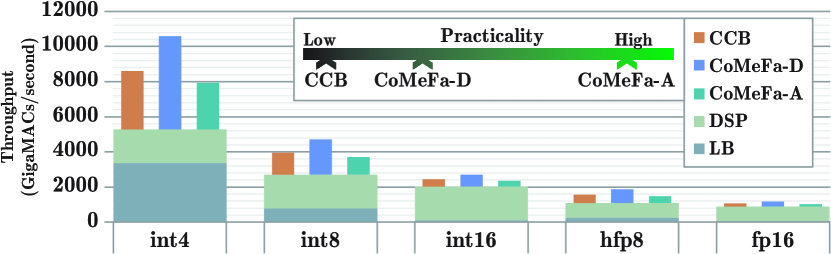
To evaluate the peak throughput, we consider the MAC (multiply-accumulate) operation, which is the most common operation in DSP and DL applications. We use common fixed-point precisions - 4-bit (accumulator=16-bit), 8-bit (acc=27-bit) and 16-bit (acc=36-bit), as well as floating-point precisions - HFP8 ({exp=4, frac=3} and acc={exp=6, frac=9}) [38] and IEEE FP16 (acc=IEEE FP32). We compare the throughput of CoMeFa RAMs to the traditional compute units (LBs and DSPs). For LBs, we synthesize, place and route one MAC onto the FPGA and determine the operating frequency and resource utilization. We then calculate the throughput by optimistically assuming that we can fill the FPGA at the same operating frequency. This serves the purpose for evaluating peak throughput. For DSPs, MACs are created and taken through a similar process. The DSPs do not natively support FP16 and HFP8 precisions, so MACs for these precisions are designed using soft logic and DSPs. For CoMeFa RAMs, 160 MACs are implemented in parallel by instantiating one CoMeFa RAM and an instruction generation FSM.
Figure 8 shows the peak throughput for each precision obtained from each different computing resource in GigaMACs/second. We observe that the throughput of the FPGA increases by 2x, 1.7x, 1.3x, 1.7x and 1.3x for int4, int8, int16, hfp8 and fp16 respectively by adding CoMeFa-D RAMs. Similarly, the throughput of the FPGA increases by 1.5x, 1.36x, 1.16x, 1.36x and 1.15x for int4, int8, int16, hfp8 and fp16 respectively by adding CoMeFa-A RAMs. CoMeFa RAM throughput reduces as the precision increases, due to the bit-serial nature of computation in CoMeFa RAMs. CoMeFa RAMs can be used for computing in any precision, unlike DSPs. The frequency of operation of CoMeFa RAMs does not change significantly with changing precision, unlike LBs.
V-B Speedup and Energy Benefits
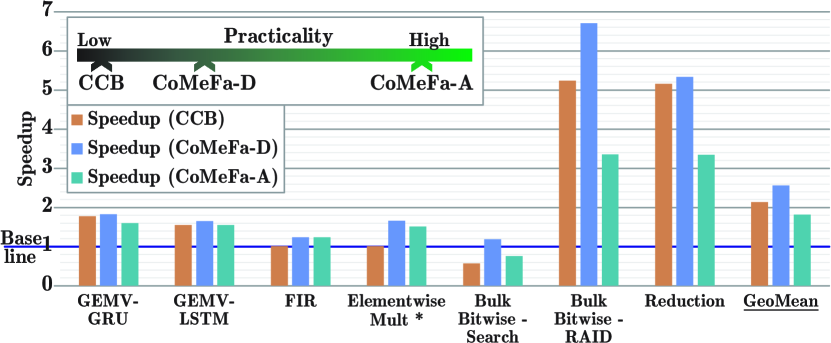
Figure 9 shows the maximum speedup obtained by using CoMeFa RAMs across benchmarks. We see significant speedups by using CoMeFa RAMs in the compute bound applications because of the augmented compute throughput provided by the FPGA. For GEMV benchmarks, speedups of upto 81% are seen in CoMeFa-D and upto 59% in CoMeFa-A. With CCB, the max speedup was 72%. We observed some erraticness in results across seeds because the DSPs were ~99% utilized, so we considered the maximum frequency instead of averaging the frequency across many seeds as we do in other applications. A speedup of 22% is seen in the FIR benchmark for both CoMeFa-D and CoMeFa-A. That’s because the frequency of operation of the overall design was ~215MHz in both cases. The FIR benchmark uses chaining of RAMs, which is not supported by CCB. So, no speedup is considered compared to the baseline.
Since the Elementwise multiplication benchmark is limited by DRAM bandwidth, no speedup is seen by using CoMeFa RAMs. CoMeFa RAMs are targeted to improve the compute throughput of the FPGA, not the DRAM bandwidth. If we remove the restriction of DRAM bandwidth and assume that all the compute units (CoMeFa RAMs as well as DSPs/LBs) can be fed with data, then speedups of 65% and 50% can be seen on CoMeFa-D and CoMeFa-A FPGAs respectively. Since CCB does not support floating-point operations, the speedup for this benchmark for CCB is shown as 0%.
The Search benchmark is sped up by 18% for CoMeFa-D. The design on baseline FPGA had the highest frequency of operation because of very simple operations done in soft logic. No speedup is seen using CoMeFa-A RAMs because of the low frequency of operation. This application is not sped up by using CCB either. CCB takes ~2x cycles compared to CoMeFa RAM because of the inflexibility of the processing elements that only support a few operations. E.g. AND operation can be done in 2 cycles in CCB, compared to 1 cycle in CoMeFa RAM. The RAID application is sped up by 6.7x in CoMeFa-D, 3.35x in CoMeFa-Aand 5.2x in CCB. The baseline frequencies were very high in this case also, but the difference in number of cycles enabled the significant speedups. The speedups for the Reduction benchmark (4-bit precision) were 5.3x in CoMeFa-D, 3.3x in CoMeFa-A and 5.1x in CCB.
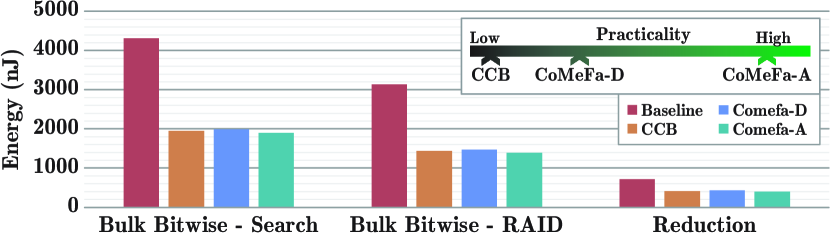
In the on-chip memory bandwidth bound benchmarks (Search, RAID, Reduction), upto 62% LBs are used in CoMeFa compared to baseline. That is because no external LUTs are needed when CoMeFa RAMs are used. Routing WL reduction of upto 68% is seen, which directly correlates to reduction in data movement. Results from our energy model are shown in Figure 10. We see an energy reduction of upto 56% in CoMeFa-A and upto 52% in CoMeFa-D.
V-C Application Co-mapping
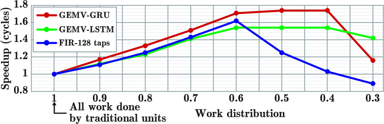
CoMeFa RAMs supplement DSPs and LBs as compute units, and enhance the FPGA’s compute throughput. Appropriately dividing and mapping parts of an application to CoMeFa RAMs and traditional compute units is key. For GEMV and FIR applications, we analytically explore the effect of varying work distribution between CoMeFa RAMs and DSPs/LBs on the proposed FPGA. The results are shown in Figure 11. We see that as more work is given to CoMeFa RAMs, more speedup can be obtained upto a limit, after which the overheads (loading, unloading, serial compute) associated with CoMeFa RAMs can start dominating and reduce the overall speedup. This sweet spot is different for each application.
V-D Adaptability to Precision
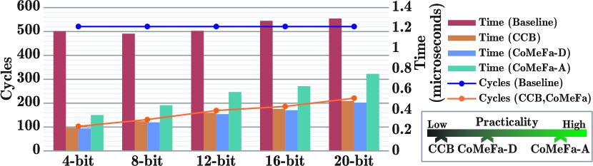
CoMeFa RAMs can be used for efficiently computing in any custom precision. Figure 12 shows the results of sweeping the precision from 4-bit to 20-bit in the Reduction benchmark. We see speedups ranging from 5.3x (3.3x) to 2.7x (1.7x) with CoMeFa-D (CoMeFa-A) as precision increases. CoMeFa-D is 3% better than CCB owing to the improved frequency achieved by the design. The baseline takes the same number of cycles for each precision because of the bit-parallel nature of compute. But the number of cycles taken increases as the precision increases when CoMeFa RAMs are used. This is because of bit-serial arithmetic and illustrates that applications using smaller precisions are better suited for CoMeFa RAMs. Note that the frequency of operation stays constant for CoMeFa RAMs because the hardware architecture stays the same. For the baseline, the frequency decreases slightly as the precision increases.
VI Conclusion
In this paper, we propose augmenting the compute density of FPGAs by modifying BRAMs into new blocks called CoMeFa RAMs, which are ideal for enhancing applications with inherent parallelism like deep learning and signal processing. To the best of our knowledge, this is the first work that (1) utilizes the dual-port nature of BRAMs to achieve in-BRAM compute, (2) deploys configurable 1-bit processing elements inside an FPGA BRAM, and (3) applies in-BRAM compute to DL and non-DL applications on FPGAs. With improvements to compute density and reduction in power consumption, we believe that converting some or all BRAMs on FPGAs to CoMeFa RAMs can be a significant step towards closing the performance gap between FPGAs and ASICs.
References
- [1] Xilinx. (2021) UltraScale Architecture Memory Resources. [Online]. Available: https://www.xilinx.com/support/documentation/user_guides/ug573-ultrascale-memory-resources.pdf
- [2] Intel, “Intel Arria 10 Device Overview,” 2021. [Online]. Available: https://www.intel.com/content/www/us/en/docs/programmable/683332/current/device-overview.html
- [3] C. Eckert et al., “Neural Cache: Bit-Serial in-Cache Acceleration of Deep Neural Networks,” in Proceedings of the 45th Annual International Symposium on Computer Architecture, ser. ISCA ’18. IEEE Press, 2018, p. 383–396. [Online]. Available: https://doi.org/10.1109/ISCA.2018.00040
- [4] A. Landy and G. Stitt, “Serial Arithmetic Strategies for Improving FPGA Throughput,” ACM Trans. Embed. Comput. Syst., vol. 16, no. 3, jul 2017. [Online]. Available: https://doi.org/10.1145/2996459
- [5] ——, “Revisiting Serial Arithmetic: A Performance and Tradeoff Analysis for Parallel Applications on Modern FPGAs,” in 2015 IEEE 23rd Annual International Symposium on Field-Programmable Custom Computing Machines, 2015, pp. 9–16.
- [6] S. Ghose, A. Boroumand, J. S. Kim, J. Gómez-Luna, and O. Mutlu, “Processing-In-Memory: A Workload-Driven Perspective,” IBM Journal of Research and Development, vol. 63, no. 6, pp. 3:1–3:19, 2019.
- [7] A. Shafiee et al., “ISAAC: A Convolutional Neural Network Accelerator with In-Situ Analog Arithmetic in Crossbars,” in 2016 ACM/IEEE 43rd Annual International Symposium on Computer Architecture (ISCA), 2016, pp. 14–26.
- [8] P. Chi et al., “PRIME: A Novel Processing-in-Memory Architecture for Neural Network Computation in ReRAM-Based Main Memory,” in 2016 ACM/IEEE 43rd Annual International Symposium on Computer Architecture (ISCA), 2016, pp. 27–39.
- [9] M. Imani, S. Gupta, Y. Kim, and T. Rosing, “FloatPIM: In-Memory Acceleration of Deep Neural Network Training with High Precision,” in Proceedings of the 46th International Symposium on Computer Architecture, 2019, p. 802–815.
- [10] S. Li, D. Niu, K. T. Malladi, H. Zheng, B. Brennan, and Y. Xie, “DRISA: A DRAM-based Reconfigurable In-Situ Accelerator,” in 2017 50th Annual IEEE/ACM International Symposium on Microarchitecture (MICRO), 2017, pp. 288–301.
- [11] V. Seshadri, D. Lee, T. Mullins, H. Hassan, A. Boroumand, J. Kim, M. A. Kozuch, O. Mutlu, P. B. Gibbons, and T. C. Mowry, “Ambit: In-Memory Accelerator for Bulk Bitwise Operations Using Commodity DRAM Technology,” in 2017 50th Annual IEEE/ACM International Symposium on Microarchitecture (MICRO), 2017, pp. 273–287.
- [12] F. Gao, G. Tziantzioulis, and D. Wentzlaff, “ComputeDRAM: In-Memory Compute Using Off-the-Shelf DRAMs,” in Proceedings of the 52nd Annual IEEE/ACM International Symposium on Microarchitecture, ser. MICRO ’52. New York, NY, USA: Association for Computing Machinery, 2019, p. 100–113. [Online]. Available: https://doi-org.ezproxy.lib.utexas.edu/10.1145/3352460.3358260
- [13] M. Kang, M.-S. Keel, N. R. Shanbhag, S. Eilert, and K. Curewitz, “An energy-efficient VLSI architecture for pattern recognition via deep embedding of computation in SRAM,” in 2014 IEEE International Conference on Acoustics, Speech and Signal Processing (ICASSP), 2014, pp. 8326–8330.
- [14] A. Agrawal, A. Jaiswal, C. Lee, and K. Roy, “X-SRAM: Enabling In-Memory Boolean Computations in CMOS Static Random Access Memories,” IEEE Transactions on Circuits and Systems I: Regular Papers, vol. 65, no. 12, pp. 4219–4232, 2018.
- [15] M. Kang, S. K. Gonugondla, and N. R. Shanbhag, “Deep In-Memory Architectures in SRAM: An Analog Approach to Approximate Computing,” Proceedings of the IEEE, vol. 108, no. 12, pp. 2251–2275, 2020.
- [16] J. Wang, X. Wang, C. Eckert, A. Subramaniyan, R. Das, D. Blaauw, and D. Sylvester, “A 28-nm Compute SRAM With Bit-Serial Logic/Arithmetic Operations for Programmable In-Memory Vector Computing,” IEEE Journal of Solid-State Circuits, vol. 55, no. 1, pp. 76–86, 2020.
- [17] D. Elliott, M. Stumm, W. Snelgrove, C. Cojocaru, and R. Mckenzie, “Computational RAM: implementing processors in memory,” IEEE Design Test of Computers, vol. 16, no. 1, pp. 32–41, 1999.
- [18] S. Jeloka et al., “A 28 nm Configurable Memory (TCAM/BCAM/SRAM) Using Push-Rule 6T Bit Cell Enabling Logic-in-Memory,” IEEE Journal of Solid-State Circuits, vol. 51, no. 4, pp. 1009–1021, 2016.
- [19] X. Wang, V. Goyal, J. Yu, V. Bertacco, A. Boutros, E. Nurvitadhi, C. Augustine, R. Iyer, and R. Das, “Compute-Capable Block RAMs for Efficient Deep Learning Acceleration on FPGAs,” in 2021 IEEE 29th Annual International Symposium on Field-Programmable Custom Computing Machines (FCCM), 2021, pp. 88–96.
- [20] D. Lewis, D. Cashman, M. Chan, J. Chromczak, G. Lai, A. Lee, T. Vanderhoek, and H. Yu, “Architectural Enhancements in Stratix V,” in Proceedings of the ACM/SIGDA International Symposium on Field Programmable Gate Arrays, ser. FPGA ’13. New York, NY, USA: Association for Computing Machinery, 2013, p. 147–156. [Online]. Available: https://doi.org/10.1145/2435264.2435292
- [21] J. Tyhach et al., “Arria 10 Device Architecture,” in 2015 IEEE Custom Integrated Circuits Conference (CICC), 2015, pp. 1–8.
- [22] S. Yazdanshenas, K. Tatsumura, and V. Betz, “Don’t Forget the Memory: Automatic Block RAM Modelling, Optimization, and Architecture Exploration,” in Proceedings of the 2017 ACM/SIGDA International Symposium on Field-Programmable Gate Arrays, ser. FPGA ’17. New York, NY, USA: Association for Computing Machinery, 2017, p. 115–124. [Online]. Available: https://doi.org/10.1145/3020078.3021731
- [23] S. Aga, S. Jeloka, A. Subramaniyan, S. Narayanasamy, D. Blaauw, and R. Das, “Compute Caches,” in 2017 IEEE International Symposium on High Performance Computer Architecture (HPCA), 2017, pp. 481–492.
- [24] A. Subramaniyan, J. Wang, E. R. M. Balasubramanian, D. Blaauw, D. Sylvester, and R. Das, “Cache Automaton,” in Proceedings of the 50th Annual IEEE/ACM International Symposium on Microarchitecture, ser. MICRO-50 ’17. New York, NY, USA: Association for Computing Machinery, 2017, p. 259–272. [Online]. Available: https://doi.org/10.1145/3123939.3123986
- [25] K. E. Murray, O. Petelin, S. Zhong, J. M. Wang, M. ElDafrawy, J.-P. Legault, E. Sha, A. G. Graham, J. Wu, M. J. P. Walker, H. Zeng, P. Patros, J. Luu, K. B. Kent, and V. Betz, “VTR 8: High Performance CAD and Customizable FPGA Architecture Modelling,” ACM Trans. Reconfigurable Technol. Syst., 2020.
- [26] S. Yazdanshenas and V. Betz, “COFFE2: Automatic Modelling and Optimization of Complex and Heterogeneous FPGA Architectures,” ACM Transactions on Reconfigurable Technology and Systems (TRETS), vol. 12, no. 1, pp. 3:1–3:27, January 2019.
- [27] A. S. University. (2012) Predictive Technology Model. [Online]. Available: http://ptm.asu.edu/
- [28] NCSU. (2018) FreePDK45. [Online]. Available: https://www.eda.ncsu.edu/wiki/FreePDK45:Contents
- [29] S. W. Keckler, W. J. Dally, B. Khailany, M. Garland, and D. Glasco, “GPUs and the Future of Parallel Computing,” IEEE Micro, vol. 31, no. 5, pp. 7–17, 2011.
- [30] A. Stillmaker and B. Baas, “Scaling equations for the accurate prediction of CMOS device performance from 180 nm to 7 nm,” Integration, the VLSI Journal, vol. 58, pp. 74–81, 2017, http://vcl.ece.ucdavis.edu/pubs/2017.02.VLSIintegration.TechScale/.
- [31] Intel, “Intel Arria 10 Product Table,” 2021. [Online]. Available: https://www.intel.cn/content/dam/www/programmable/us/en/pdfs/literature/pt/arria-10-product-table.pdf
- [32] ——, “Intel Arria 10 Transceiver PHY User Guide,” 2021. [Online]. Available: https://www.intel.cn/content/dam/www/programmable/us/en/pdfs/literature/hb/arria-10/ug_arria10_xcvr_phy.pdf
- [33] ——, “Hybrid Memory Cube Controller IP Core User Guide v16.0,” 2016. [Online]. Available: https://www.intel.com/content/www/us/en/docs/programmable/683854/16-0/introduction.html
- [34] A. Arora, A. Boutros, D. Rauch, A. Rajen, A. Borda, S. A. Damghani, S. Mehta, S. Kate, P. Patel, K. B. Kent, V. Betz, and L. K. John, “Koios: A Deep Learning Benchmark Suite for FPGA Architecture and CAD Research,” in 2021 31st International Conference on Field-Programmable Logic and Applications (FPL), 2021.
- [35] Intel, “Intel Arria 10 Device Datasheet,” 2020. [Online]. Available: https://www.intel.com.tw/content/dam/www/programmable/us/en/pdfs/literature/hb/arria-10/a10_datasheet.pdf
- [36] S. Narang. (2016) Baidu deepbench. [Online]. Available: https://svail.github.io/DeepBench/
- [37] Altera, “Designing Filters for High Performance,” 2015. [Online]. Available: https://www.intel.cn/content/dam/www/programmable/us/en/pdfs/literature/wp/wp-01260-stratix10-designing-filters-for-high-performance.pdf
- [38] X. Sun et al., “Hybrid 8-bit Floating Point (HFP8) Training and Inference for Deep Neural Networks,” in Advances in Neural Information Processing Systems, vol. 32. Curran Associates, Inc., 2019. [Online]. Available: https://proceedings.neurips.cc/paper/2019/file/65fc9fb4897a89789352e211ca2d398f-Paper.pdf