Anisotropic and tunable optical conductivity of a two-dimensional semi-Dirac system in the presence of elliptically polarized radiation
Abstract
We investigate the effect of ellipticity ratio of the polarized radiation field on optoelectronic properties of a two-dimensional (2D) semi-Dirac (SD) system. The optical conductivity is calculated within the energy balance equation approach derived from the semiclassical Boltzmann equation. We find that there exists the anisotropic optical absorption induced via both the intra- and interband electronic transition channels in the perpendicular and directions. Furthermore, we examine the effects of the ellipticity ratio, the temperature, the carrier density, and the band-gap parameter on the optical conductivity of the 2D SD system placed in transverse and vertical directions, respectively. It is shown that the ellipticity ratio, temperature, carrier density, and band-gap parameter can play the important roles in tuning the strength, peak position, and shape of the optical conductivity spectrum. The results obtained from this study indicate that the 2D SD system can be a promising anisotropic and tunable optical and optoelectronic material for applications in innovative 2D optical and optoelectronic devices, which are active in the infrared and terahertz bandwidths.
I Introduction
The isolation of a single layer of graphite, known as graphene exhibits an unique Dirac-like linear and gapless band structure in low-energy regime, has emerged as an important and promising field of research in condensed matter physics and electronics since 2004 Novoselov04 . The rise of newly developed two-dimensional (2D) electronic materials such as silicene, monolayer (ML) transition metal dichalcogenides (TMDs), ML hexagonal boron nitride (-BN), ML black phosphorus (BP), etc., are expected to lead to applications in next generation of high-performance nano-electronic, optical and optoelectronic devices Li17 . Recently, a distinct class of 2D materials named 2D semi-Dirac (SD) electronic systems have been realized in materials or device systems such as TiO2/V2O3 superlattices Pardo09 ; Banerjee09 , phosphorene under pressure Rodin14 , doped Guan14 or electrically modulated systems Rudenko15 ; Dutreix16 , -(BEDT-TTF)2I3 salts under pressure Kobayashi11 ; Suzumura13 , etc. Notably, SD fermions have an anisotropic band structure dispersion which displays a linear dispersion along one direction and a quadratic dispersion along the perpendicular direction Pyatkovskiy16 ; Mawrie19R . This anisotropy in the electronic band structure results in unusual physical properties as compared to, e.g., graphene and TMD-based 2D electron gas systems. This has drawn the attention of the scientific research community in recent years.
Several investigations of the electronic and optical properties of 2D SD systems have been carried out recently. In particular, the electronic, optoelectronic, and transport properties such as Floquet band structure Chen18 ; Islam18 , optical conductivity Mawrie19 ; Carbotte19 ; Carbotte19s ; Sanderson18 , dielectric function and plasmons Pyatkovskiy16 , nonlinear response Dai19 , and ballistic transport modulated by magnetic and electrical barriers Zhu21 have been studied. It has been shown that the 2D SD system can transform from normal insulator to the Chern insulating phase under light irradiation with relatively high frequencies Saha16 ; Sengupta21 . Moreover, in the presence of a high magnetic field, the 2D SD system can exhibit interesting features, such as an unusual magnetic field dependence of the Landau levels Dietl08 , the Hofstadter’s butterfly Delplace10 ; Sinha20 , Landau-Zener oscillations Saha17 , etc. Theoretical results on the thermoelectric properties, e.g., the Seebeck coefficient, the Ettingshausen coefficient, and the Righi-Leduc effect suggest that 2D SD systems can also be utilized for device applications in quantum thermoelectrics Mawrie19R ; Sengupta21 .
Experimentally, SD electrons in strained black phosphorus (BP) thin films have been realized Makino17 . The zero mode of the Landau level expected at the Dirac point has been successfully observed in magneto-resistance measurements of -(BEDT-TTF)2I3 under high hydrostatic pressure Tajima09 . Theoretical studies found a relatively large anisotropy between the optical conductivities and in the 2D plane of the system Carbotte19 ; Mawrie19 . The polarization function has also been evaluated. Within the random phase approximation (RPA), it was found that there exists an undamped anisotropic collective mode with square-root dispersion relation Banerjee12 ; Pyatkovskiy16 . On the basis of the unique anisotropic band structure and of the optical properties reported, one can predict that the polarization of the radiation light should affect the optical response of the 2D SD system. It was shown that the 2D SD system realized from few-layer black phosphorus at critical surface doping with potassium can exhibit linear and quadratic bands along the armchair and zigzag directions, respectively Kim15 ; Baik15 . Thus, this is an easy way to probe the anisotropic optical properties of the 2D SD system through a geometrical device setting.
From the viewpoint of physics, the optical conductivity is a key physical quantity, which relates directly to measurable optical coefficients such as transmittance and/or reflectivity Mak08 . On the other hand, through optical transmission or reflection experiments we can measure the optical conductivity in a 2D SD system under different experimental conditions by varying the ellipticity ratio of the polarized radiation light, temperature, carrier density, etc. In this theoretical study, we consider a 2D SD system placed in an anisotropic geometry along different directions. The optical conductivity or absorption under elliptically polarized light radiation with different ellipticity ratios is examined. We find that the optical absorption differs when the sample position is rotated by degrees. The ellipticity ratio, temperature, carrier density and band-gap parameter can effectively tune the optical absorption in the 2D SD system, especially in terahertz (THz, 1 THz 4.1 meV) and infrared regime. Thus, from a basic physics and a device application points of view, the results from this study show that the 2D SD system can be employed for the investigating of novel optoelectronic physics with corresponding applications in innovative 2D optical and optoelectronic devices.
The present paper is organized as follows. In Sec. II, we evaluate the optical conductivity of the 2D SD system placed in different directions in the framework of the energy balance equation derived from the semiclassical Boltzmann equation in the presence of an elliptically polarized radiation field. The optical transition channels for different doping levels are considered and the optical conductivities obtained under different experimental conditions are presented and discussed in Sec. III. Our main conclusions from this study are summarized in Sec. IV.
II Theoretical Framework
In this study, we consider a 2D SD system positioned in the - plane (taken as the 2D plane). The effective two band model Hamiltonian Pyatkovskiy16 ; Baik15 ; Mawrie19 ; Mawrie19R for a carrier (an electron or a hole) in reciprocal space can be written as
| (1) |
where is the carrier wave vector or momentum operator, the quadratic dispersion is along the direction, is the Fermi velocity, with being the effective carrier mass along the direction, is the band gap between the conduction and valence bands when and 2D SD would be a gapless system when with being the band-gap parameter, , and is the angle between and the axis.
The corresponding Schrödinger equation for 2D SD system can be solved analytically. The eigenvalues and eigenfunctions are given respectively by
| (2) |
where refers to conduction/valence band, and
| (3) |
with
We now consider that an elliptically polarized CW radiation field Zhang18 is applied normal to the 2D plane of the 2D SD system. Within the Coulomb gauge, the vector potential of the light field is given by the Jones vector Pedrotti17 with the left () and right () handed elliptically polarization, with an ellipticity ratio , is
| (4) |
where with and being respectively the electric field strength and the frequency of the radiation field. For the case of relatively weak radiation, the carrier-photon interaction Hamiltonian can be written as
| (7) |
where and . Thus, taking as a perturbation and applying Fermi’s golden rule, the first-order contribution to the steady-state electronic transition rate induced by direct carrier-photon interaction can be obtained as
| (8) |
where sign in the Delta function refers to the absorption () or emission () of a photon with energy , and
After the rotation of the sample coordinates or of the light polarization by , the vector potential of the radiation field now becomes
| (9) |
The carrier-photon interaction Hamiltonian is then given by
| (12) |
and the corresponding electronic transition rate is obtained as
| (13) |
In this paper, we use the Boltzmann equation approach to study the response of the carriers in a 2D SD system to the applied radiation field. For nondegenerate statistics, the semiclassical Boltzmann equation takes the form Xu10
| (14) |
where counts for the spin degeneracy, is the statistical energy distribution for the carriers such as the Fermi-Dirac function, and is the chemical potential (or Fermi energy at zero temperature) for electrons or holes in conduction or valence bands. Taking the first moment, the energy-balance equation can be derived by multiplying to both sides of the Boltzmann equation Xu10 . From the energy-balance equation, we obtain the energy transfer rate:
| (15) |
where . The optical conductivity can be obtained by Xu10 : which have intra- and interband electronic transition channels
| (16) |
We now consider an -type 2D SD system irradiated by an elliptically polarized CW radiation field. When photon energy is larger than the band gap between the conduction and valence bands, the photo-excited carriers are induced in the conduction and valence bands and a quasi-equilibrium state is established in the system. In this case, the electron density is with being the dark electron density and the photo-induced electron density. Due to charge conservation, the hole density in the system is . Furthermore, the channels of the optical absorption can be induced by intraband electronic transitions within the conduction and valence bands via the mechanism of free-carrier absorption and by interband transitions from valence band to conduction band. The interband electronic transition from conduction band to valence band via optical absorption is physically impossible. Taking the real part of the vector potential induced by polarized radiation field along the direction, the optical conductivity via different transition channels can be obtained as
| (17) |
| (18) |
and
| (19) |
respectively.
Here, the function will be replaced by a Lorentzian distribution under the energy relaxation approximation for intraband transitions: , where is the width of the broadened energy state with being the energy relaxation time.
Taking the real part of the vector potential induced by the polarized radiation field along the direction, the optical conductivity via the different transition channels are given as
| (20) |
| (21) |
and
| (22) |
From Eqs. (II)–(II), we can obtain the following relations with
| (23) |
and
| (24) |
where and are the longitudinal optical conductivities in and directions for different electronic transition channels. The interband part of the longitudinal optical conductivity and can be written respectively as
| (25) |
where
| (28) |
with
The step functions is defined as
| (29) |
and should be real and positive, which writes
| (32) |
where and . Moreover, The interband part of the longitudinal optical conductivity in direction is given by
| (33) |
where
| (36) |
with
III Results and discussions
For our numerical calculations, we take the following typical material parameters obtained from literatures: , where is the rest electron mass, and the Fermi velocity m/s Saha16 ; Mawrie19 ; Mawrie19R . However, the material parameters would differ within different materials such as , m/s in (TiO2)5/(VO2)3 and , m/s in -(BEDT-TTF)2I3 Saha17 . We use the electronic relaxation time ps for calculations of the optical conductivity induced by intraband electronic transitions. The chemical potentials (or Fermi energies) in the conduction and valence bands in a 2D SD system can be determined respectively by using the condition of carrier number conservation with the given electron and hole densities ( for conduction band and for valence band) through
| (37) |
where is the Fermi-Dirac function for electrons in conduction band or holes in valence band.
It should be noted that the electronic relaxation time depends on the carrier densities and temperature via electron-electron and electron-phonon interactions. We take a phenomenological parameter for showing the features of the intraband optical conductivity. The relaxation time could be obtained from experiments via, e.g., transport measurement Bandurin16 or ultra fast optical spectroscopy Sun08 . By the way, in the framework of Fermi’s golden rule, the optical conductivities obtained in this study corresponds to the optical absorption in a relative weak elliptically polarized radiation because a strong nonlinear optical response in a 2D SD system would be occurred in the strong terahertz radiation Dai19 ; Samal21 .
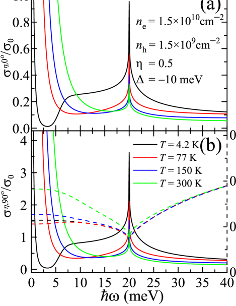
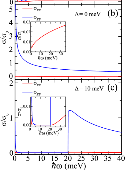
In Fig. 1, we plot the optical conductivity and as a function of photon energy at fixed ellipticity ratio, carriers density, temperature, and band-gap parameter. The total optical conductivity is due to both the inter- and the intraband transition channels. For , we obtain that the longitudinal optical conductivities along different directions are and . The optical absorption is anisotropic for both interband transitions and intraband transitions. From Eqs. (II) and (II), we learn that the optical conductivities are independent upon the sign index for left- or right-handed elliptically polarized light, which means that the transverse or Hall optical conductivity in a 2D SD system is zero. In Figs. 1(a-c), the longitudinal optical conductivity is larger than in the whole spectrum regime. At high radiation frequencies, the optical absorption in the direction is significant stronger than that in the direction, which is in line with the results obtained previously Mawrie19 ; Carbotte19 ; Carbotte19s . In the low-frequency regime, both and decrease monotonously with increasing , a typical feature of the Drude-like optical conductivity for free carriers Xiao16 . It should be noted that in Refs. Carbotte19 ; Carbotte19s , Carbotte . had also calculated the longitudinal optical conductivity of 2D semi-Dirac system in and directions with/without a gap within a Kubo formalism. Carbotte . provided separate analytic formulas of optical conductivity for intraband and interband transitions for certain limitation cases and considered the transport properties such as dc conductivity, thermal conductivity, and the Lorenz number. In Fig. 1(a), we note that an absorption peak can be observed at a photon energy meV. In Fig. 1(b), the interband optical conductivities and at low-temperature behavior as and , respectively, as obtained in Ref. Carbotte19 . In Fig. 1(c), we can see the cutoff in 20 meV is due to the prohibition of interband transitions below the band gap. In general, the results of longitudinal optical conductivities shown in Fig. 1 are in line with the results obtained in Refs. Carbotte19 ; Carbotte19s ; Mawrie19 . The van Hove singularity of in Fig. 1(a) can be understood from the electronic density-of-states (DoS). In Fig. 2, we show the DoS for a 2D SD system with different band-gap parameters. The DoS per unit area is determined by the imaginary part of the Green’s function via
| (38) |
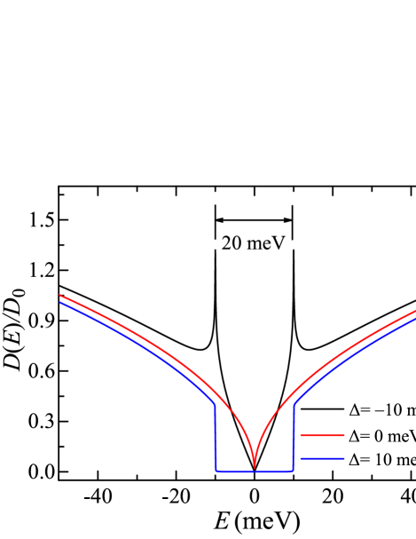
where is the retarded Green’s functions for a carrier in the band and is the electron energy. We take a broadened width of meV with replacing the delta function with energy relation approximation. From Fig. 2, we see that the DoS for a 2D SD system differs significantly from that for a semiconductor-based 2D electron gas, which is a step-function, and from that for graphene, which is linear. The DoS for the 2D SD system depends strongly on the band-gap parameter . For a band-gap parameter of meV, we see that the energy spacing between the two peaks in DoS is 20 meV, which corresponds to an electronic transition energy of 20 meV and, thus, results in a strong absorption peak in optical conductivity as shown in Fig. 1(a). For the case of the DoS for a 2D SD system increases nonlinearly with starting from the band edges. As a result, the interesting features of the DoS for a 2D SD system are the main reasons why the corresponding optoelectronic properties are different from semiconductor-based 2D electron gas systems and from graphene.
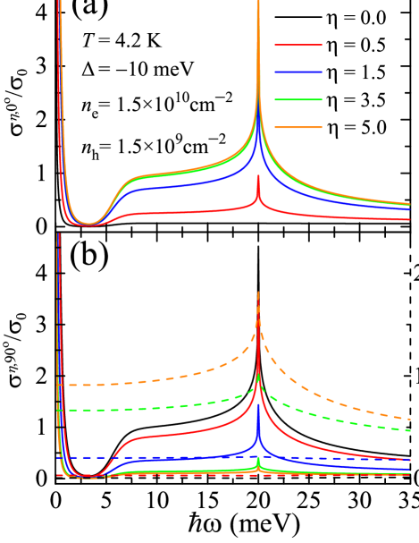
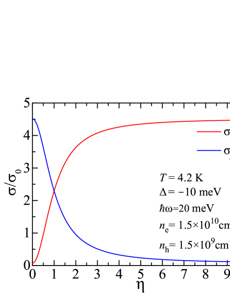
In Fig. 3, the optical conductivities in (a) and in (b) are shown as a function of radiation photon energy at a fixed band-gap parameter, temperature, carrier densities for different values of the ellipticity ratios . With increasing ellipticity ratio, the values of the optical conductivity in longitudinal direction increases in the whole spectral regime and the optical conductivity in the vertical direction decreases. From Fig. 3(b), we can also see that the ratio of the optical conductivity between longitudinal and vertical directions, , increases with increasing . In Fig. 4, we plot the peak hight of the optical conductivity in Fig. 3 at a photon energy 20 meV as a function of ellipticity ratio. We can see that the peak hight of increases/decreases with increasing the ellipticity ratio. The absorption peak hight in van Hove singularity can be effectively tuned by the ellipticity ratio. In the presence of elliptically polarized light with different ellipticity ratios, the 2D SD system shows a strong anisotropy on the optical absorption. Hence, the ellipticity ratio of light radiation can effectively tune the optical and optoelectronic properties of the 2D SD system in the infrared and THz regime.
In Fig. 5, we show the effect of temperature on the optical conductivity spectrum of the 2D SD system at the fixed band-gap parameter, ellipticity ratio, and carrier densities. In the long-wavelength regime where the free-carrier absorption contributes mainly to the intra-band transitions, the optical absorption increases with increasing temperature. In the intermediate frequency regime, the absorption near the absorption peak is stronger at low temperature. For photon energies meV, the effect of temperature on the optical conductivity or absorption is weak. However, the ratio of the optical conductivities in different directions becomes larger at higher temperatures, which implies that anisotropic optical absorption can already be observed at room temperature.
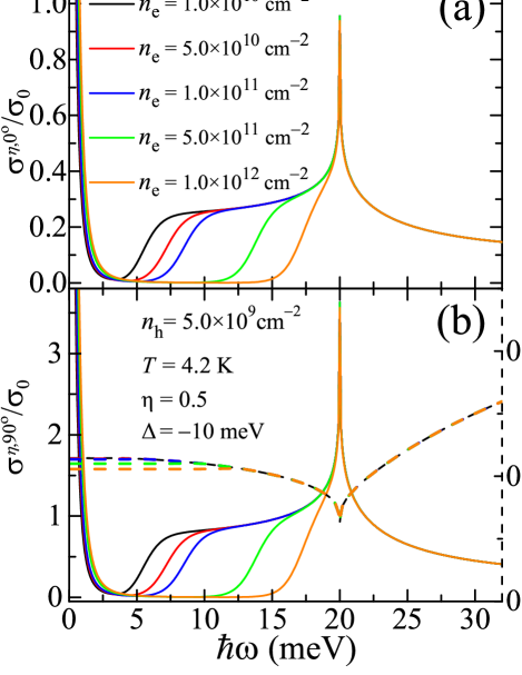
In Fig. 6, we plot the optical conductivities and as a function of photon energy at the fixed band-gap parameter, temperatures, ellipticity ratio, hole density for different electron densities. With increasing the electron density, the absorption edges in the optical conductivities or absorption spectra show a blue shift and the absorption at high frequency is not affected by the variation of the electron density. This phenomenon is a result of the well known Pauli-blocking effect Grigorenko12 , which indicates that electronic transitions can only occur from occupied states to empty states at low temperatures. With increasing electron density, the Fermi energy in conduction band increases. This can increase the energy separation between the occupied valence band states and the empty conduction band states and, thus, result in the blue shift in the optical absorption edge. Similar to conventional electronic devices, the carrier density and chemical potential in a 2D SD system can also be tuned, e.g., by applying a gate voltage. As can be see, the absorption regime becomes narrow with increasing electron density. Thus, a wider absorption spectrum can be observed in lower-density samples.
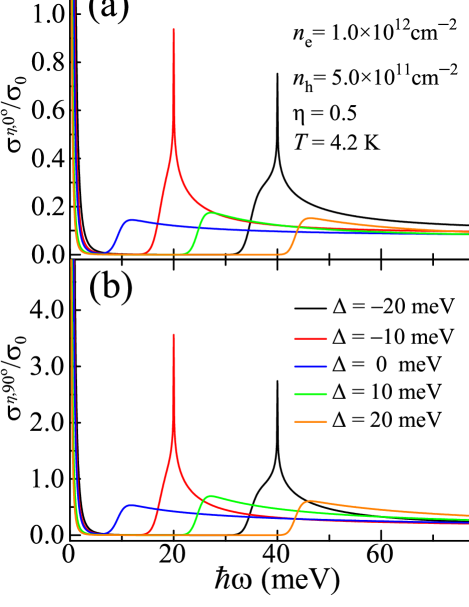
In Fig. 7, we show the optical conductivities and as a function of photon energy at the fixed temperature, ellipticity ratio, carrier densities for different band-gap parameters. With changing the band gap parameter, the strength and the position of the optical absorption in infrared and THz regime can be effectively tuned in the presence of an elliptically polarized light field. From Eq. (2), we know that the 2D SD system has a band-gap when . At the fixed carrier concentrations, the absorption edge in Fig. 7 exhibits a blue shift for larger band-gap parameter. For a negative band-gap parameter , the 2D SD system is gapless and presents unique two nodal points in the energy spectrum Mawrie19 ; Pyatkovskiy16 . The absorption edge is also blue shifted with decreasing . It has been shown that there exists a widely tunable band gap in few-layer black phosphorus doped with potassium using an surface doping technique Kim15 or by the induction of strain Kim21 . Using such band-gap engineering approaches Kim15 ; Chaves20 , the anisotropic optical absorption can be effectively tuned in the infrared and THz bandwidths.
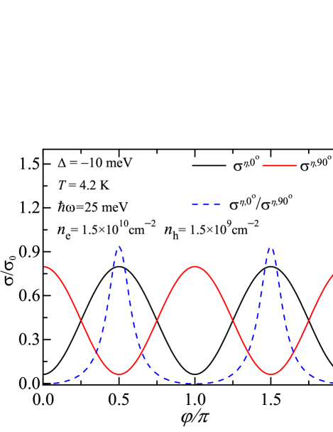
In Fig. 8, we plot the optical conductivities and along different directions and their ratio as a function of the ellipticity angle at the fixed radiation photon energy meV, temperature, band-gap parameter, and carriers densities. The sinusoidal and the cosinusoidal like behaviors appear for respectively and when varying the ellipticity angle from 0 to . The strongest optical absorption of can be seen with the ellipticity angles at and and the strongest absorption along the perpendicular direction can be observed with the ellipticity angles at and . There exists a phase displacement of when the sample is rotated with at a certain ellipticity angle. The strongest effect in the anisotropy in the optical conductivities and can be achieved at the ellipticity angles and . We expect that such an interesting feature in the ellipticity dependence of the optical absorption in a 2D SD system can be observed experimentally through conventional infrared or THz transmission measurement with elliptical polarizers.
In this study, we considered a 2D SD system with a device setting placed in directions perpendicular to each other. Hereby, the anisotropic and tunable optical absorption can be achieved by tuning the ellipticity ratio of the polarized radiation light. As we know, a large difference in optical absorption can also be transformed into electrical signals. As a result, 2D SD systems can be used in infrared and THz optoelectronic devices. Moreover, we find that the effect of temperature, carrier density and band-gap parameter can also modify significantly the optical and optoelectronic properties of the 2D SD system. Due to the unique anisotropic and tunable optical conductivity, the 2D SD system can be promising materials for applications in optics and optoelectronics in infrared and THz bandwidths.
IV Conclusions
In this paper, we presented a detailed theoretical study on the anisotropic and tunable optical conductivity of 2D SD systems in the presence of elliptically polarized light irradiation. By considering the electron-photon interaction using Fermi’s gold rule, the optical conductivity was evaluated using the energy balance equation approach derived from the semi-classical Boltzmann equation. The effects of the ellipticity ratio of the polarized radiation field, temperature, carrier density, and band-gap parameter on the optical conductivity was examined theoretically. The main conclusions we have obtained from this study are summarized as follows.
2D SD systems exhibit anisotropic optical conductivity or optical absorption within the bandwidth from THz to infrared in different geometrical directions. This interesting phenomenon is induced by the anisotropy of the electronic band structure of the system. In the presence of elliptically polarized radiation field, the optical absorption can be effectively tuned by the ellipticity ratio and the ratio of the optical conductivities along the longitudinal and vertical directions , which increases with increasing ellipticity ratio of the polarized radiation fields. Therefore, by changing the ellipticity ratio, the optical signals can be effectively detected through a device setting based on the 2D SD materials. The ratio of increases with temperature, which indicates that this effect can be very likely observed even at room temperature. With increasing the carrier density, the optical absorption edge is blue shifted, which is caused by the Pauli-blocking effects Grigorenko12 . Using band-gap engineering Kim15 ; Chaves20 , the band structure of the 2D SD system can be turned by changing the band-gap parameter resulting in a tuning of the optical absorption in infrared and THz bandwidths.
From our theoretical results, we have found that the optical and optoelectronic properties of the 2D SD systems can be effectively tuned by the ellipticity ratio, temperature, carrier density, and band-gap parameter. The 2D semi-Dirac systems can therefore be applied as tunable optical and optoelectronic materials to be used for the realization of such devices as optical modulators, switches, polarizers etc., which are active in the infrared to THz bandwidths. Moreover, It has been shown that 2D SD electronic systems can be obtained in materials such as multilayer (TiO2)m/(VO2)n heterostructures Pardo09 ; Banerjee09 , -(BEDT-TTF)2I3 Kobayashi11 ; Suzumura13 , few-layer black phosphorus Makino17 ; Baik15 , silicene oxide Zhong17 , etc. By controlling the ellipticity of THz or infrared polarized radiation with elliptical polarizers, the elliptically dependence optical conductivity in this study can be measured through the techniques such as Fourier transform infrared (FTIR) spectroscopy and THz TDS measurement Kuzmenko08 ; Li08n ; Arts18 ; Whelan20 . Since the 2D SD materials mentioned above are usually predicted theoretically. It is worth mentioning that our theoretical results would also be helpful for detecting the 2D SD electrons in these materials. We hope that our theoretical predictions can be verified experimentally in the near.
ACKNOWLEDGMENTS
This work was supported by the National Natural Science foundation of China (NSFC) (Grants No. 12004331, No. U1930116, No. U1832153, No. U206720039, No. 11847054), Shenzhen Science and Technology Program (No. KQTD20190929173954826), and by Yunnan Fundamental Research Projects (No. 2019FD134). B.V.D. was supported through a post doc fellowship from the Research Foundation Flanders (FWO-V1).
References
- (1) K. S. Novoselov, A. K. Geim, S. V. Morozov, D. Jiang, Y. Zhang, S. V. Dubonos, I. V. Grigorieva, and A. A. Firsov, Science 306, 666 (2004).
- (2) X. Li, L. Tao, Z. Chen, H. Fang, X. Li, X. Wang, J.-B. Xu, and H. Zhu, Appl. Phys. Rev. 4, 021306 (2017).
- (3) V. Pardo and W. E. Pickett, Phys. Rev. Lett. 102, 166803 (2009).
- (4) S. Banerjee, R. R. P. Singh, V. Pardo, and W. E. Pickett, Phys. Rev. Lett. 103, 016402 (2009).
- (5) A. S. Rodin, A. Carvalho, and A. H. C. Neto, Phys. Rev. Lett. 112, 176801 (2014).
- (6) J. Guan, Z. Zhu, and D. Tománek, Phys. Rev. Lett. 113, 046804 (2014).
- (7) A. N. Rudenko, S. Yuan, and M. I. Katsnelson, Phys. Rev. B 92, 085419 (2015).
- (8) C. Dutreix, E. A. Stepanov, and M. I. Katsnelson, Phys. Rev. B 93, 241404(R) (2016).
- (9) A. Kobayashi, Y. Suzumura, F. Piéchon, and G. Montambaux, Phys. Rev. B 84, 075450 (2011).
- (10) Y. Suzumura, T. Morinari, and F. Pichon, J. Phys. Soc. Jpn. 82, 023708 (2013).
- (11) P. K. Pyatkovskiy and T. Chakraborty, Phys. Rev. B 93, 085145 (2016).
- (12) A. Mawrie and B. Muralidharan, Phys. Rev. B 100, 081403(R) (2019).
- (13) Q. Chen, L. Du, and G. A. Fiete, Phys. Rev. B 97, 035422 (2018).
- (14) SKFiroz Islam and A. Saha, Phys. Rev. B 98, 235424 (2018).
- (15) A. Mawrie and B. Muralidharan, Phys. Rev. B 99, 075415 (2019).
- (16) J. P. Carbotte, K. R. Bryenton, and E. J. Nicol, Phys. Rev. B 99, 115406 (2019).
- (17) J. P. Carbotte and E. J. Nicol, Phys. Rev. B 100, 035441 (2019).
- (18) M. Sanderson, S. Huang, Y. Zhang, and C. Zhang, J. Phys. D: Appl. Phys. 51 205302 (2018).
- (19) X. Dai, L. Liang, Q. Chen, and C. Zhang, J. Phys.: Condens. Matter 31, 135703 (2019).
- (20) X. Zhu, W. Chen, X. Zhou, X. Xiao, and G. Zhou, Physica E 126, 114462 (2021).
- (21) P. Sengupta and L. A. Jauregui, J. Appl. Phys. 130, 054303 (2021).
- (22) K. Saha, Phys. Rev. B 94, 081103(R) (2016).
- (23) P. Dietl, F. Piéchon, and G. Montambaux, Phys. Rev. Lett. 100, 236405 (2008).
- (24) P. Sinha, S. Murakami, and S. Basu, Phys. Rev. B 102, 085416 (2020).
- (25) P. Delplace and G. Montambaux, Phys. Rev. B 82, 035438 (2010).
- (26) K. Saha, R. Nandkishore, and S. A. Parameswaran, Phys. Rev. B 96, 045424 (2017).
- (27) T. Makino, Y. Katagiri, C. Ohata, K. Nomura, and J. Haruyama, RSC Adv. 7, 23427 (2017).
- (28) N. Tajima, S. Sugawara, R. Kato, Y. Nishio, and K. Kajita, Phys. Rev. Lett. 102, 176403 (2009).
- (29) S. Banerjee and W. E. Pickett, Phys. Rev. B 86, 075124 (2012).
- (30) S. S. Baik, K. S. Kim, Y. Yi, and H. J. Choi, Nano Lett. 15(12), 7788-7793 (2015).
- (31) J. Kim, S. S. Baik, S. H. Ryu, Y. Sohn, S. Park, B.g-G. Park, J. Denlinger, Y. Yi, H. J. Choi, and K. S. Kim, Science 349(6249), 723-726 (2015).
- (32) K. F. Mak, M. Y. Sfeir, Y. Wu, C. H. Lui, J. A. Misewich, and T. F. Heinz, Phys. Rev. Lett. 101, 196405 (2008).
- (33) X. Zhang, W. Liao, H. Bao, and M. Zuo, Appl. Phys. A 124:354 (2018).
- (34) Frank L. Pedrotti, Leno M. Pedrotti, and Leno S. Pedrotti, Introduction to Optics (Cambridge University Press, Cambridge, 2017).
- (35) W. Xu, H. M. Dong, L. L. Li, J. Q. Yao, P. Vasilopoulos, and F. M. Peeters, Phys. Rev. B 82, 125304 (2010).
- (36) D. A. Bandurin, I. Torre, R. K. Kumar, M. B. Shalom, A. Tomadin, A. Principi, G. H. Auton, E. Khestanova, K. S. Novoselov, and I. V. Grigorieva, Science 351, 1055 (2016).
- (37) D. Sun, Z.-K. Wu, C. Divin, X. Li, C. Berger,W. A. de Heer, P. N. First, and T. B. Norris, Phys. Rev. Lett. 101, 157402 (2008).
- (38) S. S. Samal, S. Nandy, and K. Saha, Phys. Rev. B 103, L201202 (2021).
- (39) Y. M. Xiao, W. Xu, B. Van Duppen, and F. M. Peeters, Phys. Rev. B 94, 155432 (2016).
- (40) A. N. Grigorenko, M. Polini, and K. S. Novoselov, Nat. Photon. 6, 749 (2012).
- (41) H. Kim, S. Z. Uddin, D.-H. Lien, M. Yeh, N. S. Azar, S. Balendhran, T. Kim, N. Gupta, Y. Rho, C. P. Grigoropoulos, K. B. Crozier, and A. Javey, Nature (London) 596, 232 (2021).
- (42) A. Chaves, J. G. Azadani, H. Alsalman, D. R. da Costa, R. Frisenda, A. J. Chaves, S. H. Song, Y. D. Kim, D. He, J. Zhou et al., npj 2D Mater. Appl. 4, 29 (2020).
- (43) C. Zhong, Y. Chen, Y. Xie, Y.-Y. Sun, and S. Zhang, Phys. Chem. Chem. Phys. 19, 3820 (2017).
- (44) A. B. Kuzmenko, E. van Heumen, F. Carbone, and D. van der Marel, Phys. Rev. Lett. 100, 117401 (2008).
- (45) Z. Q. Li, E. A. Henriksen, Z. Jiang, Z. Hao, M. C. Martin, P. Kim, H. L. Stormer, and D. N. Basov, Nature Phys. 4, 532 (2008).
- (46) K. Arts, R. Vervuurt, A. Bhattacharya, J. G. Rivas, J. W. Oosterbeek, and A. A. Bol, J. Appl. Phys. 124, 073105 (2018).
- (47) P. R Whelan, Q. Shen, B. Zhou, I G Serrano, M V. Kamalakar, D. M A Mackenzie, J. Ji, D. Huang, H. Shi, D. Luo et al., 2D Mater. 7, 035009 (2020).