Single-shot readout of multiple donor electron spins with a gate-based sensor
Abstract
Proposals for large-scale semiconductor spin-based quantum computers require high-fidelity single-shot qubit readout to perform error correction and read out qubit registers at the end of a computation. However, as devices scale to larger qubit numbers integrating readout sensors into densely packed qubit chips is a critical challenge. Two promising approaches are minimising the footprint of the sensors, and extending the range of each sensor to read more qubits. Here we show high-fidelity single-shot electron spin readout using a nanoscale single-lead quantum dot (SLQD) sensor that is both compact and capable of reading multiple qubits. Our gate-based SLQD sensor is deployed in an all-epitaxial silicon donor spin qubit device, and we demonstrate single-shot readout of three 31P donor quantum dot electron spins with a maximum fidelity of 95%. Importantly in our device the quantum dot confinement potentials are provided inherently by the donors, removing the need for additional metallic confinement gates and resulting in strong capacitive interactions between sensor and donor quantum dots. We observe a scaling of the capacitive coupling between sensor and 31P dots (where is the sensor-dot distance), compared to in gate-defined quantum dot devices. Due to the small qubit size and strong capacitive interactions in all-epitaxial donor devices, we estimate a single sensor can achieve single-shot readout of approximately 15 qubits in a linear array, compared to 3-4 qubits for a similar sensor in a gate-defined quantum dot device. Our results highlight the potential for spin qubit devices with significantly reduced sensor densities.
I Introduction
High-fidelity single-shot spin readout is an essential requirement for large-scale spin-based quantum computing proposals [1, 2]. In spin qubit devices readout has most commonly been performed by mapping the spin state onto a charge state, which can then be detected using a nearby charge sensor [3, 4]. The most sensitive charge sensors to date are radio-frequency single-electron transistors (rf-SETs) which have demonstrated integration times for a signal-to-noise (SNR) ratio of 1 of ns [5] (we use to directly compare sensor performance between experiments, see Supplementary S1). However rf-SETs require at least three gate leads to operate, a significant space allocation on the qubit chip as devices scale to larger qubit numbers. In contrast gate-based (or dispersive) sensors integrate qubit readout capability into the existing leads used for qubit control, allowing spin measurements without additional proximal charge sensors [6, 7, 8, 9]. Single-shot readout using dispersive sensors has recently been demonstrated [10, 11, 12, 13, 14], however these results relied on Pauli blockade between two spins for readout, requiring an additional quantum dot (with associated control leads) for spin detection. Furthermore, in each case readout of only a single qubit was achieved. Dispersive sensors which probe inter-dot transitions (referred to here as “direct dispersive” sensors) can also only generate signal at an inter-dot charge transition, a small window in gate space. Experiments to date have thus often used a secondary multi-lead charge sensor for device characterisation [10, 11].
The SLQD is a gate-based sensor that combines the benefits of rf-SETs and direct dispersive sensors [15]. It requires only a single lead to operate, improving scalability prospects over the rf-SET, yet can also perform readout directly in the single-spin basis. The SLQD is sensitive over a wide range of device voltages, and has been used as a compact sensor for single-electron charge detection in quantum dot arrays [16, 17, 18], as well as time-averaged single-spin measurements [19].
In this work we deploy a SLQD charge sensor in a device containing four 31P donor quantum dots. We use the SLQD to perform single-shot electron spin readout in the single-spin basis on three out of the four quantum dots, achieving a maximum readout fidelity of 95%. The fourth quantum dot was found to have a tunnel rate exceeding the measurement bandwidth (300 kHz) and could not be projectively measured. We achieve an amplitude signal to noise ratio of 9.6 at 15 kHz measurement bandwidth, yielding ns. This compares favourably to previous dispersive readout measurements operating with off-chip resonators at 100-300 MHz frequencies [10, 11, 12] (respectively , and ).
Importantly we find that for our donor device the detection range of the sensor is extended compared to gate-defined quantum dot architectures. Charge sensor range is determined by the capacitive coupling between the sensor and the readout target, which in our device follows a dependence as a function of sensor-qubit distance, . Previous reports in undoped planar SiGe devices observed a dependence [20, 21], and in nanowire CMOS devices a dependence was estimated based on device simulations [18]. In free space the capacitive coupling between isolated charges scales as , however this scaling is modified by the presence of surrounding gates and becomes for charges underneath a large metal plane [21], as is the case for gate-defined devices operated in accumulation mode [22, 23]. In atomically engineered donor devices the qubit trapping potential is defined naturally by the donor, eliminating the need for additional accumulation gates and resulting in extremely low gate densities. The reduced screening in atomic precision donor devices considerably extends charge sensor range. We estimate that our current sensor would be able to read out approximately 15 donor qubits in a linear array with high fidelity, compared to 3-4 for a sensor with similar performance in a gate-defined quantum dot device.
II Device and sensor operation
The four 31P quantum dot device is fabricated on a silicon substrate using atomic precision hydrogen resist lithography [24, 25]. Figure 1 (a) shows an STM image of the device, with sites D1, D2, D3 and D4 indicating regions where phosphorus donors are incorporated to host electron spin qubits [26]. R1 and R2 serve as electron reservoirs for (D1, D2) and (D3, D4) respectively, as well as providing electrostatic tuning of the donor potentials.
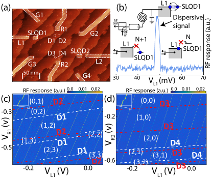
G1 and G2 are electrostatic gates used for readout pulse sequences on D1 and D2, and G3 and G4 serve the same purpose for D3 and D4. SLQD1 and SLQD2 are charge sensors for determining the electron occupation of the donor dots, and to perform single-shot spin readout via spin to charge conversion.
A schematic of the operating principle of the SLQD sensor is shown in Fig. 1 (b). The sensor detects the extra quantum capacitance [6, 8, 9] added to the circuit when the Fermi energy of L1 aligns with an available charge state on SLQD1, resulting in Coulomb-like peaks that can be used for charge sensing. We note that in this work SLQD1 is used for all measurements. Figures 1 (c),(d) show charge stability diagrams for the top (D1, D2) and bottom (D3, D4) pairs of donor quantum dots, respectively. The periodic diagonal lines in the data are Coulomb-like peaks from SLQD1, where donor charge transitions are observed as breaks in these lines aligned along the labelled dotted lines overlaying the data. We identify transitions from all four patterned donor quantum dots from the distinct transition line slopes, shown in Fig. 1 (c) (D1 white dashed lines, D2 red dashed lines) and Fig. 1 (d) (D3 red dashed lines, D4 white dashed lines). Electron numbers are assigned by fully depleting the donors of electrons, then adding an electron each time a donor transition line is crossed. We note that sweeping R1 (R2) to negative voltages adds electrons to D1 and D2 (D3 and D4), in contrast to sweeping gates that are only capacitively coupled (and not tunnel-coupled), for which negative voltages typically remove electrons. These plots demonstrate the ability of SLQD1 to characterise the charge occupation of all four quantum dots.
III Single-shot spin readout
We next use SLQD1 to perform single-shot electron spin readout in the single-spin basis for D1, D2 and D3 at B=1.5 T. We note that for D4 the tunnel rate to R2 exceeded our measurement bandwidth and readout could not be performed. Figure 2 (a) shows a gate-gate map sweeping and over a single SLQD1 line intersecting with the first electron charge transition of D1. Adding an electron to D1 shifts the SLQD1 peak position by mV (where is the mutual charging voltage in terms of ). We perform spin readout with a three-level pulse sequence consisting of a load phase to initialise a random electron spin state, followed by a read phase where the spin is projectively measured, and an empty phase to eject the electron before the next pulse repetition [4]. During the read phase a spin up state will tunnel to R1 followed by a spin down tunnelling back to D1, generating a characteristic “blip” in the charge sensor response which is absent for a spin down state. Figure 2 (b) shows example spin up and spin down traces for D1, demonstrating single-shot readout. We calculate the spin readout fidelity by taking 5000 individual single-shot traces and find (see Supplementary S3 for full details of the fidelity analysis). The fidelity is limited by our measurement bandwidth (set to ~80 kHz), which was not high enough to capture the fastest tunnelling events. Increasing the measurement bandwidth permits faster events at the cost of reduced SNR (which also decreases the fidelity [27]), and we found 80 kHz to give the maximum fidelity of 81%.
Figure 2 (c) shows a gate-gate map at the second electron of D2. Here we performed readout [28] due to the favourable electron tunnel rate at the second electron transition (~2.6 kHz). Example single-shot traces are shown in Fig. 2 (d), and taking 5000 individual traces we find a fidelity of for D2. This fidelity is again limited in part by our finite measurement bandwidth (here 15 kHz) filtering the fastest tunnelling events, as well as a relatively high electron temperature (~280 mK). We note the electron temperature was not raised by the reflectometry signal applied to SLQD1 until significantly higher powers than used in our experiments. Figure 2 (e) shows a gate-gate map at the first electron of D3. In this case electrons tunnel between D3 and R2 (rather than R1 as in the previous cases) during spin readout. Figure 2 (f) shows corresponding example single-shot traces for D3, and here we find a fidelity of , which is limited by the same factors as D2.
Figure 2(g) shows a gate-gate map at the first electron transition of D4. Here we found that the D4-R2 tunnel rate exceeded our measurement bandwidth (~300 kHz, limited by the resonator bandwidth), and we were not able to perform readout on this donor. In fact, a faint dispersive signal can be observed due to cyclical tunneling of an electron between D4 and R2 (shown in Fig. 2 (h)), implying that this tunnel rate is a non-negligible fraction of the ~130 MHz reflectometry drive signal. Table 1 summarises our spin readout results, with a maximum fidelity of 95%. By lowering the electron temperature to mK, using a higher frequency resonant circuit and lower noise first-stage amplifier, readout of D1, D2 and D3 with 99% fidelity is achievable [27, 28, 29].
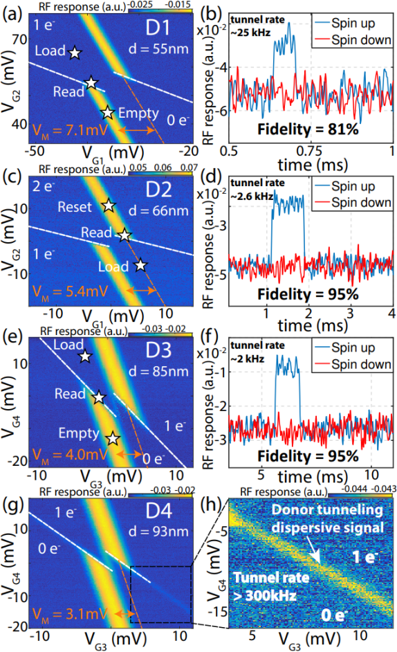
| Donor number | Readout transition electron # | Tunnel rate (kHz) | Distance to sensor (nm) | Sensor shift (mV) | Readout fidelity (%) | Measurement bandwidth (kHz) | Amplitude SNR | (ns) | |
| D1 | 2P | 01 | ~25 | 55 | 7.1 | 81 | 80 | 4.0 | 780 |
| D2 | 3P | 12 | ~2.6 | 66 | 5.4 | 95 | 15 | 9.6 | 720 |
| D3 | 3P | 01 | ~2.0 | 85 | 4.0 | 95 | 15 | 8.1 | 1020 |
| D4 | 1P | 01 | 300 | 93 | 3.1 | N/A | N/A | N/A | N/A |
IV Long-range charge sensing
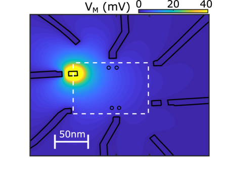
We next investigate the scaling of the SLQD1 sensor shift as a function of the sensor-qubit distance . We used the finite element package COMSOL multiphysics to simulate for the device in Fig. 1 (a) (Supplementary S4). Figure 3 (a) plots the simulated profile, with the colourscale showing the expected for a qubit at the corresponding position. determines the SLQD1 peak shift due to a charging event on the target qubit, and is proportional to the capacitive coupling between sensor and qubit. The white dashed contour line in Fig. 3 (a) indicates the region within which is large enough to shift the SLQD1 Coulomb peak from full signal (on top of the peak) to % signal due to a charging event on the target qubit (the strong response threshold). Any qubit located inside the footprint of this contour would generate full on-off switching of the sensor signal [14], and could be measured without any loss of fidelity due to the distance from the sensor.
Figure 3 (b) plots the simulated as a function of (the distance from the center of SLQD1) for the device region containing the sensor and patterned qubits (Supplementary S4). Fitting to the simulated values we find , which is consistent with the measured data (shown by red circles). Both our experimental and simulated results are consistent with a scaling, in contrast to the scaling observed in planar gate-defined devices [20, 21], indicated by the yellow curve in Fig. 3 (b).

Figure 3 (c) highlights the impact this difference in scaling has for long-range charge sensing. The left panel uses the fit from Fig. 3 (b) to estimate at distances of 100, 200 and 300 nm from the sensor. The solid blue and red dotted lines show the expected position of the SLQD Coulomb peak for 0 electrons and 1 electron on the target qubit at the specified distance. The shape of the sensor Coulomb peak is determined by fitting the experimental data. The vertical black arrows indicate the maximum sensor contrast for detecting the electron charge on the target. The right panel uses the fit from Fig. 3 (b) to estimate for 100, 200 and 300 nm from the sensor. In this case decreases more rapidly with distance, and the contrast is minimal at 300 nm.
To highlight the importance of this roll-off for scalable quantum computing, we calculate the expected single-shot readout fidelity as a function of for a qubit with the same spin-dependent tunnel rates and T1 time as D3 in our device. We extrapolate the fit in Fig. 3 (b) to estimate as a function of , and use this to calculate the expected signal contrast. We can then calculate the SNR using the noise measured in our experiment and input this to our fidelity calculation (Supplementary S5). Figure 3 (d) shows the result for both (blue curve) and (orange curve). As expected the curve exhibits a faster roll-off in readout fidelity. For small both red and blue curves saturate to 95% fidelity as observed in our direct experimental measurements of D3. We find that a qubit with the same properties as D3 could be measured with over 90% spin readout fidelity up to 300 nm from the sensor, compared to 130 nm for the scaling. We predict that the estimated 90% readout fidelity at 300 nm for our current sensor could be increased to 99% by reducing the electron temperature [28], operating the SLQD at higher frequencies and using a lower noise first-stage amplifier [29].
With a 300 nm sensor range, the small size of donor qubits means that a single sensor has the potential to serve a large number of qubits. A leading proposal for a donor-based surface code architecture uses a donor separation distance of 30 nm [1]. Linear arrays are the current experimental state of the art in semiconductor spin qubits; for a linear array of donor qubits with an inter-qubit separation of 30 nm, our results suggest that we would be able to read out 20 donor qubits with high fidelity with SLQD1 placed in the center of the array. To verify the predicted qubit number that could be sensed we directly simulated a realistic linear array of donor qubits (see Supplementary S6), from which we found that sensing 14-16 qubits is feasible using our current SLQD sensor. For the geometry and scaling expected in an accumulation-mode gate-defined device (, assuming a qubit separation of 80 nm and sensor range of 130 nm), the equivalent number is 4. This is consistent with current experimental demonstrations having 3-4 qubits per sensor [20, 30]. Table 2 compares our result to recently reported single-lead sensing literature, demonstrating the significant improvement in the number of possible qubits per sensor in a linear array (see Supplementary S5 for further details).
Given the extremely long relaxation times in donor qubits (we measured ~9 s for D3 at 2.5 Tesla, and up to 30 s has been demonstrated [31]) and recent advances navigating charge states in large qubit arrays [30, 32], 15 qubits similar to D3 could be measured sequentially by the same sensor within the relaxation time. We note that reducing the electron temperature would narrow the SLQD Coulomb peaks, increasing the charge detection signal for small shifts and further extending the sensor range (and thus number of qubits measured) beyond our current estimate. We also note that donor qubits can be placed significantly closer than 30 nm using atomic precision lithography. For an architecture of tunnel coupled donors (typically separated by 10-15 nm), a single optimised SLQD sensor could conceivably serve a linear array of 50-100 donor qubits.
V Conclusion
In conclusion, we have demonstrated single-shot electron spin readout in the single-spin basis using a SLQD charge sensor. In a device with four 31P donor quantum dots we performed single-shot readout on three of the four quantum dots with fidelities of 81%, 95% and 95%. We found that due to the low gate density in our atomic precision donor device, the capacitive coupling between sensor and qubits follows a dependence compared to the dependence observed in gate-defined devices that accumulate qubit electrons below metallic gates. As a consequence charge sensor range is significantly extended in our device compared to such gate-defined devices. Because of this extended range and the small size of donor qubits, we estimate that our current sensor could projectively measure ~15 donor spin qubits in a linear array. Our results highlight the prospect of large-scale quantum computing architectures with significantly reduced sensor densities in atom-scale spin qubits.
| Reference | Sensor type | Device type | Max spin readout fidelity | Readout basis | Estimated capacitive scaling | Estimated qubits per sensor | |
| Pakkiam et. al., (2018) [10] | s | Direct dispersive | Precision donor | 83% | Singlet/ triplet | 1 | |
| West et. al., (2019) [11] | s | Direct dispersive | Planar MOS | 73% | Singlet/ triplet | 1 | |
| Zheng et. al., (2019) [13] | 170 ns | Direct dispersive | SiGe | 98% | Singlet/ triplet | 1 | |
| Urdampiletta et. al., (2019) [12] | s | Latched SLQD | Nanowire MOS | 98% | Singlet/ triplet | 1-3 | |
| Chanrion et. al., (2020) [16] | s | SLQD | Nanowire MOS | N/A | N/A | 3 | |
| Ansaloni et. al., (2020) [17] | s | SLQD | Nanowire MOS | N/A | N/A | 3 | |
| Cirano-Tejel et. al., (2020) [19] | s | SLQD | Nanowire MOS | N/A | Single spin | 3 | |
| Duan et. al., (2020) [18] | s | SLQD | Nanowire MOS | N/A | N/A | 3 | |
| Hogg et. al., (this work) | 720 ns | SLQD | Precision donor | 95% | Single spin | 15 |
VI Methods
Device fabrication The device is fabricated on a p-type natural Si substrate (1-10cm) using an STM to perform atomic precision hydrogen resist lithography [33]. A fully terminated H:Si(2) reconstructed surface is prepared in an ultra-high vacuum chamber (~ mbar). The STM tip is used to selectively remove hydrogen atoms to create a lithographic mask which defines the device. The regions of desorbed hydrogen are n-doped with 31P by introducing a gaseous precursor into the chamber, which adsorbs to the silicon surface only where the hydrogen has been removed. Subsequent annealing (at 350) incorporates the 31P atoms into the silicon crystal. Removing only a few hydrogen atoms allows the fabrication of atomic-scale donor quantum dots. The device is then encapsulated with 50 nm of silicon, grown by molecular beam epitaxy. The resulting structure consists of the qubit device embedded in crystalline silicon. The device is then removed from the STM chamber and contacted electrically with aluminium ohmic contacts though etched via holes.
Measurement details The device chip is bonded to a PCB to deliver high-frequency signals and DC voltages then mounted to the cold finger of a dilution refrigerator with ~80 mK base temperature. We use a NbTiN superconducting spiral inductor for reflectometry measurements, with a resonance frequency of ~130 MHz and a loaded quality factor of ~400 when bonded to L1. An AC signal is first attenuated before being applied to L1, with the reflected signal being separated to the output chain using a directional coupler, before amplification (at 4K using a CITLF3 low-noise amplifier, and at room temperature with a Pasternack PE15A1012), demodulation (Polyphase AD0105B) and acquisition with a digitiser card (NI-USB-6363). Spin readout pulse sequences are generated by an AWG (Tektronix AWG5204).
VII Acknowledgements
This research was conducted by the Australian Research Council Centre of Excellence for Quantum Computation and Communication Technology (project number CE170100012) and Silicon Quantum Computing Pty Ltd. MYS acknowledges an Australian Research Council Laureate Fellowship. The device was fabricated in part at the NSW node of the Australian National Fabrication Facility (ANFF).
VIII Author contributions
MRH conceived the project and designed the device with input from PP. MRH fabricated the device with assistance from YC. MRH performed the measurements and data analysis with input from MGH. AVT designed and fabricated the superconducting inductor used for reflectometry. SKG calculated the spin readout fidelities. GKG assisted with the spin relaxation measurements. PP and MRH performed the COMSOL modelling. MRH, SKG and MYS wrote the manuscript with input from MGH. MGH and MYS supervised the project.
IX Author information
Correspondence and requests for materials should be addressed to MYS (michelle.simmons@unsw.edu.au).
X Competing financial interests
MYS is a director of the company Silicon Quantum Computing Pty Ltd. All other authors declare no competing financial interests.
References
- Hill et al. [2015] C. D. Hill, E. Peretz, S. J. Hile, M. G. House, M. Fuechsle, S. Rogge, M. Y. Simmons, and L. C. Hollenberg, A surface code quantum computer in silicon, Science Advances 1, 1 (2015).
- Veldhorst et al. [2017] M. Veldhorst, H. G. J. Eenink, C. H. Yang, and A. S. Dzurak, Silicon cmos architecture for a spin-based quantum computer, Nature Communications 8, 1766 (2017).
- Elzerman et al. [2004] J. M. Elzerman, R. Hanson, L. H. Willems van Beveren, B. Witkamp, L. M. K. Vandersypen, and L. P. Kouwenhoven, Single-shot read-out of an individual electron spin in a quantum dot, Nature 430, 431 (2004).
- Morello et al. [2010] A. Morello, J. J. Pla, F. A. Zwanenburg, K. W. Chan, K. Y. Tan, H. Huebl, M. Möttönen, C. D. Nugroho, C. Yang, J. A. van Donkelaar, A. D. C. Alves, D. N. Jamieson, C. C. Escott, L. C. L. Hollenberg, R. G. Clark, and A. S. Dzurak, Single-shot readout of an electron spin in silicon, Nature 467, 687 (2010).
- Keith et al. [2019a] D. Keith, M. G. House, M. B. Donnelly, T. F. Watson, B. Weber, and M. Y. Simmons, Single-shot spin readout in semiconductors near the shot-noise sensitivity limit, Phys. Rev. X 9, 041003 (2019a).
- Petersson et al. [2010] K. D. Petersson, C. G. Smith, D. Anderson, P. Atkinson, G. A. C. Jones, and D. A. Ritchie, Charge and spin state readout of a double quantum dot coupled to a resonator, Nano Letters 10, 2789 (2010).
- Colless et al. [2013] J. I. Colless, A. C. Mahoney, J. M. Hornibrook, A. C. Doherty, H. Lu, A. C. Gossard, and D. J. Reilly, Dispersive readout of a few-electron double quantum dot with fast rf gate sensors, Phys. Rev. Lett. 110, 046805 (2013).
- House et al. [2015] M. G. House, T. Kobayashi, B. Weber, S. J. Hile, T. F. Watson, J. van der Heijden, S. Rogge, and M. Y. Simmons, Radio frequency measurements of tunnel couplings and singlet–triplet spin states in si:p quantum dots, Nature Communications 6, 8848 (2015).
- Gonzalez-Zalba et al. [2015] M. F. Gonzalez-Zalba, S. Barraud, A. J. Ferguson, and A. C. Betz, Probing the limits of gate-based charge sensing, Nature Communications 6, 6084 (2015).
- Pakkiam et al. [2018] P. Pakkiam, A. V. Timofeev, M. G. House, M. R. Hogg, T. Kobayashi, M. Koch, S. Rogge, and M. Y. Simmons, Single-Shot Single-Gate rf Spin Readout in Silicon, Physical Review X 8, 041032 (2018), arXiv:1809.01802 .
- West et al. [2019] A. West, B. Hensen, A. Jouan, T. Tanttu, C. H. Yang, A. Rossi, M. F. Gonzalez-Zalba, F. Hudson, A. Morello, D. J. Reilly, and A. S. Dzurak, Gate-based single-shot readout of spins in silicon, Nature Nanotechnology 14, 437 (2019), arXiv:1809.01864 .
- Urdampilleta et al. [2019] M. Urdampilleta, D. J. Niegemann, E. Chanrion, B. Jadot, C. Spence, P.-A. Mortemousque, C. Bäuerle, L. Hutin, B. Bertrand, S. Barraud, R. Maurand, M. Sanquer, X. Jehl, S. De Franceschi, M. Vinet, and T. Meunier, Gate-based high fidelity spin readout in a cmos device, Nature Nanotechnology 14, 737 (2019).
- Zheng et al. [2019] G. Zheng, N. Samkharadze, M. L. Noordam, N. Kalhor, D. Brousse, A. Sammak, G. Scappucci, and L. M. Vandersypen, Rapid gate-based spin read-out in silicon using an on-chip resonator, Nature Nanotechnology 14, 742 (2019).
- Borjans et al. [2021] F. Borjans, X. Mi, and J. Petta, Spin digitizer for high-fidelity readout of a cavity-coupled silicon triple quantum dot, Phys. Rev. Applied 15, 044052 (2021).
- House et al. [2016] M. G. House, I. Bartlett, P. Pakkiam, M. Koch, E. Peretz, J. van der Heijden, T. Kobayashi, S. Rogge, and M. Y. Simmons, High-sensitivity charge detection with a single-lead quantum dot for scalable quantum computation, Phys. Rev. Applied 6, 044016 (2016).
- Chanrion et al. [2020] E. Chanrion, D. J. Niegemann, B. Bertrand, C. Spence, B. Jadot, J. Li, P.-A. Mortemousque, L. Hutin, R. Maurand, X. Jehl, M. Sanquer, S. De Franceschi, C. Bäuerle, F. Balestro, Y.-M. Niquet, M. Vinet, T. Meunier, and M. Urdampilleta, Charge detection in an array of cmos quantum dots, Phys. Rev. Applied 14, 024066 (2020).
- Ansaloni et al. [2020] F. Ansaloni, A. Chatterjee, H. Bohuslavskyi, B. Bertrand, L. Hutin, M. Vinet, and F. Kuemmeth, Single-electron operations in a foundry-fabricated array of quantum dots, Nature Communications 11, 6399 (2020).
- Duan et al. [2020] J. Duan, M. A. Fogarty, J. Williams, L. Hutin, M. Vinet, and J. J. L. Morton, Remote capacitive sensing in two-dimensional quantum-dot arrays, Nano Letters 20, 7123 (2020), pMID: 32946244, https://doi.org/10.1021/acs.nanolett.0c02393 .
- Ciriano-Tejel et al. [2021] V. Ciriano-Tejel, M. Fogarty, S. Schaal, L. Hutin, B. Bertrand, L. Ibberson, M. Gonzalez-Zalba, J. Li, Y. Niquet, M. Vinet, and J. Morton, Spin readout of a cmos quantum dot by gate reflectometry and spin-dependent tunneling, PRX Quantum 2, 010353 (2021).
- Zajac et al. [2016] D. M. Zajac, T. M. Hazard, X. Mi, E. Nielsen, and J. R. Petta, Scalable gate architecture for a one-dimensional array of semiconductor spin qubits, Phys. Rev. Applied 6, 054013 (2016).
- Neyens et al. [2019] S. F. Neyens, E. MacQuarrie, J. Dodson, J. Corrigan, N. Holman, B. Thorgrimsson, M. Palma, T. McJunkin, L. Edge, M. Friesen, S. Coppersmith, and M. Eriksson, Measurements of capacitive coupling within a quadruple-quantum-dot array, Phys. Rev. Applied 12, 064049 (2019).
- Borselli et al. [2015] M. G. Borselli, K. Eng, R. S. Ross, T. M. Hazard, K. S. Holabird, B. Huang, A. A. Kiselev, P. W. Deelman, L. D. Warren, I. Milosavljevic, A. E. Schmitz, M. Sokolich, M. F. Gyure, and A. T. Hunter, Undoped accumulation-mode Si/SiGe quantum dots, Nanotechnology 26, 10.1088/0957-4484/26/37/375202 (2015), arXiv:1408.0600 .
- Lim et al. [2009] W. H. Lim, F. A. Zwanenburg, H. Huebl, M. Möttönen, K. W. Chan, A. Morello, and A. S. Dzurak, Observation of the single-electron regime in a highly tunable silicon quantum dot, Applied Physics Letters 95, 242102 (2009), https://doi.org/10.1063/1.3272858 .
- Simmons et al. [2005] M. Simmons, F. Ruess, K. Goh, T. Hallam, S. Schofield, L. Oberbeck, N. Curson, A. Hamilton, M. Butcher, R. Clark, and T. Reusch, Scanning probe microscopy for silicon device fabrication, Molecular Simulation 31, 505 (2005), https://doi.org/10.1080/08927020500035580 .
- Fuechsle et al. [2012] M. Fuechsle, J. A. Miwa, S. Mahapatra, H. Ryu, S. Lee, O. Warschkow, L. C. L. Hollenberg, G. Klimeck, and M. Y. Simmons, A single-atom transistor, Nature Nanotechnology 7, 242 (2012).
- He et al. [2019] Y. He, S. K. Gorman, D. Keith, L. Kranz, J. G. Keizer, and M. Y. Simmons, A two-qubit gate between phosphorus donor electrons in silicon, Nature 571, 371 (2019).
- Keith et al. [2019b] D. Keith, S. K. Gorman, L. Kranz, Y. He, J. G. Keizer, M. A. Broome, and M. Y. Simmons, Benchmarking high fidelity single-shot readout of semiconductor qubits, New Journal of Physics 21, 10.1088/1367-2630/ab242c (2019b), arXiv:1811.03630 .
- Watson et al. [2015] T. F. Watson, B. Weber, M. G. House, H. Büch, and M. Y. Simmons, High-fidelity rapid initialization and read-out of an electron spin via the single donor charge state, Phys. Rev. Lett. 115, 166806 (2015).
- Schaal et al. [2020] S. Schaal, I. Ahmed, J. A. Haigh, L. Hutin, B. Bertrand, S. Barraud, M. Vinet, C.-M. Lee, N. Stelmashenko, J. W. A. Robinson, J. Y. Qiu, S. Hacohen-Gourgy, I. Siddiqi, M. F. Gonzalez-Zalba, and J. J. L. Morton, Fast gate-based readout of silicon quantum dots using josephson parametric amplification, Phys. Rev. Lett. 124, 067701 (2020).
- Volk et al. [2019] C. Volk, A. M. J. Zwerver, U. Mukhopadhyay, P. T. Eendebak, C. J. van Diepen, J. P. Dehollain, T. Hensgens, T. Fujita, C. Reichl, W. Wegscheider, and L. M. K. Vandersypen, Loading a quantum-dot based “qubyte” register, npj Quantum Information 5, 29 (2019).
- Watson et al. [2017] T. F. Watson, B. Weber, Y.-L. Hsueh, L. C. L. Hollenberg, R. Rahman, and M. Y. Simmons, Atomically engineered electron spin lifetimes of 30 s in silicon, Science Advances 3, e1602811 (2017), https://www.science.org/doi/pdf/10.1126/sciadv.1602811 .
- Mills et al. [2019] A. R. Mills, D. M. Zajac, M. J. Gullans, F. J. Schupp, T. M. Hazard, and J. R. Petta, Shuttling a single charge across a one-dimensional array of silicon quantum dots, Nature Communications 10, 1063 (2019).
- Fuechsle et al. [2010] M. Fuechsle, S. Mahapatra, F. A. Zwanenburg, M. Friesen, M. A. Eriksson, and M. Y. Simmons, Spectroscopy of few-electron single-crystal silicon quantum dots, Nature Nanotechnology 5, 502 (2010).
- Ahmed et al. [2018] I. Ahmed, J. A. Haigh, S. Schaal, S. Barraud, Y. Zhu, C.-m. Lee, M. Amado, J. W. A. Robinson, A. Rossi, J. J. L. Morton, and M. F. Gonzalez-Zalba, Radio-frequency capacitive gate-based sensing, Phys. Rev. Applied 10, 014018 (2018).
- Stehlik et al. [2015] J. Stehlik, Y.-Y. Liu, C. M. Quintana, C. Eichler, T. R. Hartke, and J. R. Petta, Fast charge sensing of a cavity-coupled double quantum dot using a josephson parametric amplifier, Phys. Rev. Applied 4, 014018 (2015).
- Schoelkopf et al. [1998] R. J. Schoelkopf, P. Wahlgren, A. A. Kozhevnikov, P. Delsing, and D. E. Prober, The radio-frequency single-electron transistor (rf-set): A fast and ultrasensitive electrometer, Science 280, 1238 (1998).
- Rahman et al. [2007] R. Rahman, C. J. Wellard, F. R. Bradbury, M. Prada, J. H. Cole, G. Klimeck, and L. C. L. Hollenberg, High precision quantum control of single donor spins in silicon, Phys. Rev. Lett. 99, 036403 (2007).
- Laucht et al. [2015] A. Laucht, J. T. Muhonen, F. A. Mohiyaddin, R. Kalra, J. P. Dehollain, S. Freer, F. E. Hudson, M. Veldhorst, R. Rahman, G. Klimeck, K. M. Itoh, D. N. Jamieson, J. C. McCallum, A. S. Dzurak, and A. Morello, Electrically controlling single-spin qubits in a continuous microwave field, Science Advances 1, e1500022 (2015).
- Weber et al. [2012] B. Weber, S. Mahapatra, H. Ryu, S. Lee, A. Fuhrer, T. C. G. Reusch, D. L. Thompson, W. C. T. Lee, G. Klimeck, L. C. L. Hollenberg, and M. Y. Simmons, Ohm’s law survives to the atomic scale, Science 335, 64 (2012).
Supplemental Materials: Single-shot readout of multiple donor electron spins with a gate-based sensor
XI 1: Universal sensitivity metric
To be able to compare the performance of various charge sensors in the literature, we employ the integration time for a detection signal to noise ratio of 1 () as our metric. Assuming a white noise distribution, can be calculated from the amplitude signal to noise ratio between the two sensor signal levels measured for a given integration time ():
| (S1) |
where SNR is the amplitude signal to noise ratio (, with is the signal amplitude between the two sensor readout levels and one standard deviation of the noise distribution, assumed here to be white Gaussian). can thus easily be estimated based on standard experimental parameters. can be measured more accurately (at the cost of additional experimental effort) by measuring the sensor SNR for a range of and extrapolating to SNR=1.
We note that a charge sensitivity metric that has been commonly used in the semiconductor qubit community is electrons per root Hertz () [9, 34, 29, 35, 13]. However there are two distinct methods for calculating the charge sensitivity in which in general do not give equivalent results and make direct comparison between experiments difficult. The first is a frequency-domain method, where a small modulating signal is applied to a gate nearby the sensor, and the magnitude of frequency sidebands generated by the modulation signal is measured [36]. This frequency-domain method for determining the charge sensitivity in is scaled to the charging energy of the sensor (which can vary significantly between devices and different material systems) and hence cannot be directly compared between different experiments. This method also only quantifies the response of the sensor to small charge shifts (much smaller than the Coulomb peak linewidth), and is hence an inappropriate metric for strong-response regime charge sensors (where the sensor signal shifts by an appreciable fraction of a linewidth due to a charging event on a nearby qubit) [5, 16, 17, 19, 14]. Because it is scaled to the sensor charging energy, this frequency domain method is also unsuitable for sensors which do not have a periodic response in the gate charge, such as direct dispersive sensors measuring inter-dot transitions.
The second method for calculating the charge sensitivity in is to first determine , then calculate the charge sensitivity as [35, 13]
| (S2) |
Typically when using Eq. S2, is set to 1, as the charge state of the readout target is changing by a single electron. The results from this second method are however not consistent with the frequency domain method, for which indicates a shift in the sensor peak of the full sensor charging energy. As a consequence the second method thus generally gives significantly larger (i.e. worse) values of , and direct comparisons between values determined using the two different methods must be treated with caution.
For these reasons we thus explicitly use in the main text as a more useful metric than for directly comparing readout performance in semiconductor spin qubits. Not only is it applicable in both weak and strong-response regimes, but also for sensors that do not create a signal periodic in the gate charge such as dispersive senors. Table S1 therefore compares (calculated using Eq. S1 where not directly reported) for a selection of recent dispersive readout results. For reference, the current best charge sensor performance is Keith et. al. [5], who achieved ns (SNR=12.7, ns) with an rf-SET.
| Reference | SNR | Sensor type | Resonator type | Resonator frequency | Lever arm | ||
| Hogg et. al., 2020 (this work) | 66 s | 9.6 | 720 ns | SLQD | NbTiN spiral | 130 MHz | 0.380.05 (1-) |
| Pakkiam et. al., 2018 [10] | 300 s | 4 | 19s | Direct dispersive | NbTiN spiral | 335 MHz | 0.130.05 () |
| West et. al., 2019 [11] | 12 ms | 2 | 3000s | Direct dispersive | PCB inductor | 267 MHz | 0.10.03 () |
| Urdampellita et. al., 2019 [12] | 500 s | 6.5 | 8s | SLQD (latched) | PCB inductor | 234 MHz | 0.3 () |
| Zheng et. al., 2019 [13] | 170 ns | 1 | 170 ns | Direct dispersive | NbTiN on-chip | 5.7 GHz | - |
| Stehlik et al., 2015 [35] | 7 ns | 1 | 7 ns | Direct dispersive (JPA) | Nb on-chip | 7.88 GHz | - |
| Schaal et al., 2020 [29] | 80 ns | 1 | 80 ns | Direct dispersive (JPA) | NbN spiral | 622 MHz | 0.36 () |
The lever arm column in Table S1 lists the relevant lever arm factor for the dispersive sensor, which depends on the type of sensor. For example, for direct dispersive sensors the amount of signal generated depends on the differential lever arm () between the gate to which the probe rf signal is applied and the two quantum dots. For SLQD sensors the amount of signal generated depends on the lever arm of the reflectometry gate acting on the sensor dot (, or if the reflectometry gate is also the reservoir for the sensor dot). Table S1 highlights that dispersive sensor performance can be optimised by increasing the resonator frequency, using a low-noise amplifier (such as a Josephson parametric amplifier, JPA) and maximising the relevant lever arm factor.
XII 2. Optimising the sensor for single-electron charge detection
To optimise SLQD1 for the time-resolved charge detection of the donor quantum dots, the main experimental parameter we can tune is the input reflectometry power . In an SLQD the sensor signal saturates as a function of [15]. This can be understood intuitively by considering the cyclical single-electron tunnelling process that generates the dispersive signal. When is large enough to fully traverse a Coulomb peak, a full electron is driven between L1 and SLQD1 each time the reflectometry signal reverses polarity. Because there is no DC current path, the tunnelling current is limited to two electrons per AC cycle. The amplitude of the tunnelling current is thus constrained by Coulomb blockade. The measured signal is directly proportional to the tunnelling current in the device, hence this also saturates. In our measurements choosing to be at the onset of this signal saturation was optimal for readout (purple circle in Fig. S1 (d)), as we now discuss.
Figures S1 (a)-(c) show identical gate-gate maps around the first electron charge transition of D1 for three different levels. Figure S1 (a) has below the saturation level, (b) is at the onset of saturation and (c) is well into saturation. Beyond the saturation point increasing the input power does not return significantly more signal, and the Coulomb peaks start to power broaden. To sense our donor electrons, we choose the value from S1 (b), which gives an optimal balance between signal contrast and Coulomb peak power broadening.
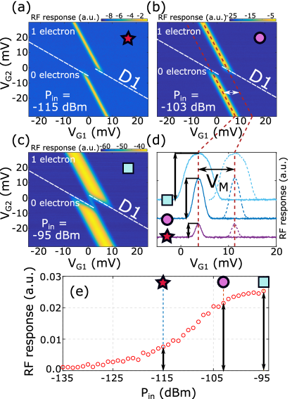
Figure S1 (d) demonstrates the shift in the SLQD1 sensor response () due to an electron charging event on D1. The size of this shift depends on the capacitive coupling between SLQD1 and the target qubit, and for D1 is mV. As discussed in the main text, the size of as a function of distance to the sensor is an important factor in determining the density of sensors required in a device. An architecture in which decreases slowly as a function of distance can reduce the number of charge sensors required. We note that due to the strong capacitive coupling between SLQD1 and D1, is larger than a Coulomb peak width for all values in Fig. S1. In this situation the maximum signal contrast for sensing D1 is thus obtained by tuning to the top of a Coulomb peak, rather than the side of a peak which would give the best small-signal sensitivity. This is called the strong-response charge sensing regime [5], and allows binary on-off switching of the full sensor signal during detection.
In our experiment all four donor quantum dots are in the strong response regime for dBm as shown in S1 (b), hence we use the same to sense all four qubits. Figure S1 (e) shows the maximum sensor contrast as a function of , with the values from (a), (b) and (c) indicated by the matching coloured shapes. For dBm the maximum signal saturates, and going above this value causes power broadening without any significant gain in signal. This further justifies our use of dBm.
XIII 3. Readout fidelity calculation
In this section we detail the method used to estimate the measurement fidelity in our experiments using the theory outlined in Keith et. al. [27]. For completeness we summarise the fidelity calculations below.
The measurement fidelity can be broken down into two different processes in the detection event. The first process is the probability that the electron tunnels to the reservoir and not the . This stage is known as state-to-charge conversion (STC) and is used to optimise the measurement time, . The second stage relates to the probability of correctly measuring a tunneling event, known as electrical detection (E) and sets our optimal threshold voltage, . From these two processes, four fidelities can be obtained for each spin state/process combination, , , , and . Using these fidelities we can calculate the individual state measurement fidelities using,
| (S3) | ||||
| (S4) |
Finally, the total measurement fidelity is the average between the two individual state fidelities,
| (S5) |
To calculate the measurement fidelity the following parameters were obtained from the experiment: and are the low and high signal levels of the SLQD respectively with corresponding noise power spectral densities (assuming white Gaussian noise) and . is the filter cut-off frequency of the sensor, is the digitising sample rate of the data acquisition hardware used in the experiment, are the tunnel times of the electrons in and out of the electron reservoir (), is the relaxation time of the state and is the external magnetic field. In Table S2 we state all the parameters and metrics used to calculate the spin readout fidelity for each quantum dot measured in the main text.
| Parameter | D1 value | D2 value | D3 value |
| -0.04530.0001 | -0.03710.0001 | -0.09860.0001 | |
| -0.03020.0001 | -0.01420.0001 | -0.06230.0001 | |
| (1.020.01) | (2.670.01) | (3.240.01) | |
| (1.080.01) | (2.720.04) | (3.630.03) | |
| 80 kHz | 15 kHz | 15 kHz | |
| 500 kHz | 50 kHz | 50 kHz | |
| 659 s | 4994 s | 74412 s | |
| 7.92.3 ms | 25426 ms | 665 ms | |
| 150.5 s | 2576 s | 2939 s | |
| 1.50.4 s | 383 ms | 11.64.0 s | |
| T | T | T | |
| (ms) | 0.310.01 | 3.10.1 | 3.40.1 |
| Vopt (arb.) | -0.03220.0001 | -0.01960.0001 | -0.07590.0003 |
| (%) | 96.11.4 | 98.80.2 | 95.00.4 |
| (%) | 99.20.5 | 98.60.2 | 98.90.1 |
| (%) | 95.30.3 | 99.10.1 | 99.70.1 |
| (%) | 69.10.9 | 92.90.1 | 95.30.1 |
| (%) | 92.80.5 | 98.00.1 | 94.90.3 |
| (%) | 68.61.2 | 91.60.3 | 94.30.2 |
| (%) | 80.71.1 | 94.80.2 | 94.60.3 |
XIV 4. COMSOL simulation of patterned device
In Fig. 3 (a) of the main text we presented simulation results showing as a function of spatial position for the device in Fig. 1 (a) of the main text. Here we provide details of the simulation, which was performed using the finite element solver COMSOL multiphysics.
The shift in the SLQD sensor Coulomb peak due to a single-electron charging event on a target qubit is determined by the mutual charging energy () between the sensor and qubit. To find we placed a charge of one electron on SLQD1 and simulated the resulting change in potential throughout the device. Here we note that the change in potential at a given spatial position when adding an electron to SLQD1 is equivalent to the change in potential at SLQD1 when adding an electron to a qubit located at . Our simulation of adding an electron to SLQD1 thus directly returns us a spatial map of the mutual charging energy throughout the device. To convert the simulated into (the mutual charging voltage in terms of ) for direct comparison with the experimental shifts from Figs. 2 (a),(c),(e),(g) in the main text, we divided by the measured G1SLQD1 lever arm . We then accounted for an observed offset between the simulation-derived results and the experimental data by calibrating the simulation results to match the experimental data at the position of D1. After this point calibration, the simulation data matched the experimental data at the positions of D2, D3 and D4, giving us confidence in the simulation method.
To obtain the plot of as a function of distance to SLQD1 shown in Fig. 3 (b) of the main text, we used the values inside the region bounded by the white dashed box in Fig. S2. We chose the device region inside the white dashed box to include the active sensing region, but avoid including regions where no donor would be patterned in a real device (e.g. directly behind gates or within ~10 nm of a gate). For each simulation point inside the white dashed box in Fig. S2, we calculated the distance from the center of SLQD1. Inside the white dashed box, we found that followed a dependence as a function of distance to SLQD1.
XV 5. Long-range readout fidelity and distant qubit sensing
To calculate the fidelity as a function of the qubit-sensor distance, we use the expected shift in sensor response for a given based on the fit in Fig. 4 (b). The maximum difference between the two peaks separated by then gives , the maximum sensor contrast as a function of . To calculate the fidelity we modify the level such that,
| (S6) |
where is the full peak height (i.e. signal contrast when is large enough that the peaks are fully separated). In determining , we use the Coulomb peak shape extracted from fitting our experimental Coulomb peaks. In this way we calculated the sensor signal contrast as a function of , the qubit-sensor distance. We then use in our fidelity calculation with the experimental spin-dependent tunnel rates and relaxation time measured for D3, which are unrelated to the qubit-sensor distance.
Table II in the main text compares single-lead sensor results from the literature, including the device type and an estimate of the number of qubits that could be read by one sensor for the specified sensor type and fabrication platform. In compiling this table we use the reported value for (or use Eq. S1 where is not explicitly stated). For the planar gate-defined devices we use the capacitive scaling that has been previously reported [20, 21], and for nanowire MOS devices we use the estimate of based on the device modelling from [18]. We note that in some of the results of ref. [18] the capacitive coupling as a function of distance was increased using metallic couplers, which we neglect in the present analysis to focus on the bare sensor range. In estimating the number of qubits per sensor we use published literature values for geometric parameters (e.g. 80 nm qubit pitch for nanowire MOS [16]). For the results in which no spin readout was performed, we assume qubit parameters identical to D3 in our device and a sensor identical to SLQD1. We then estimate the number of qubits that could be read out with fidelity based on the geometry and appropriate capacitive scaling. We assume a 2xN array of qubits for the nanowire MOS devices (as such arrays naturally form in split-gate geometries [16]), and a 1xN array for all others device types.
XVI 6. COMSOL simulation of linear array of donor qubits
In the main text we estimated that based on a simple extrapolation of the 1/ sensor capacitive scaling that we observed in our experiment, it should be feasible to read out 20 donor qubits in a linear array using a single sensor. Here we present COMSOL modelling of a linear qubit array to improve the accuracy of this estimate using a simulated device with realistic dimensions. Figure S3 (a) shows a schematic of the linear array architecture. The array contains 20 P donor quantum dots, with an inter-dot separation of 30 nm (we chose 30 nm as this is the separation used in a leading donor surface code proposal [1]). In ref. [1] qubits are encoded in the nuclear spin states of single P donors, with single-qubit gates applied using global NMR and two-qubit gates mediated by an electron magnetic dipole interaction (see ref. [1] for full details). For the array shown in Fig. S3, qubits could also potentially be encoded in electron spin states, with single-qubit gates achieved via global ESR (addressed via electric field tuning the Stark shift [37, 38]) and magnetic dipole coupling for two-qubit gates.

Gates G1-G20 provide electrostatic tuning of the donor potentials, as well as serving as electron reservoirs. Each gate serves as the reservoir for the nearest donor. A SLQD is positioned in the center of the array to sense the qubits. Figure S3 (b) shows an electrostatic simulation of (calculated using the same method described in Section S4) for the linear array architecture in Fig. S3 (a).
Here the orange contour line shows the boundary for which a qubit (with the same tunnel rates and T1 time as D3) could be read with over 90% fidelity using a sensor with the same performance as SLQD1. The dashed lines show the uncertainty bounds of the 90% fidelity contour. In Fig. S3 (b), 14-16 donors are contained within the uncertainty bounds. This direct COMSOL modelling of a donor linear array thus indicates that 14-16 donor qubits could be read out using an SLQD sensor with the same performance as our experimental sensor, slightly fewer than the ~20 estimated from extrapolating the fit in Fig. 3 (b) in the main text. We note that the linear array geometry shown in Fig. S3 (a) is fully consistent with previously demonstrated lithographic feature sizes using atomic precision fabrication techniques [39].