A Frequency-Agnostic RIS-based solution to control the Smart Radio Propagation Environment
Abstract
The disruptive reconfigurable intelligent surface (RIS) technology is steadily gaining relevance as a key element in future 6G networks. However, a one-size-fits-all RIS hardware design is yet to be defined due to many practical considerations. A major roadblock for currently available RISs is their inability to concurrently operate at multiple carrier frequencies, which would lead to redundant installations to support multiple radio access technologies (RATs).
In this paper, we introduce FABRIS, a novel and practical multi-frequency RIS design. FABRIS is able to dynamically operate across different radio frequencies (RFs) by means of frequency-tunable antennas as unit cells with virtually no performance degradation when conventional approaches to RIS design and optimization fail. Remarkably, our design preserves a sufficiently narrow beamwidth as to avoid generating signal leakage in unwanted directions and a sufficiently high antenna efficiency in terms of scattering parameters. Indeed, FABRIS selects the RIS configuration that maximizes the signal at the intended target user equipment (UE) while minimizing leakage to non-intended neighboring UEs. Numerical results and full-wave simulations validate our proposed approach against a naive implementation that does not consider signal leakage resulting from multi-frequency antenna arrays.
Index Terms:
Reconfigurable intelligent surface, multi-frequency RIS, RIS hardware designI Introduction
Reconfigurable intelligent surfaces (RISs) have the potential to drive the biggest paradigm change in classical wireless network design. By dynamically altering the propagation of the impinging signals, they transmute the nature of the wireless radio channel from the long-established tamper-proof black-box to a variable that can be optimized, thus sowing the seeds of a fully controllable and flexible smart propagation environment [1]. RISs draw modest power and have limited installation and maintenance costs, being envisioned as planar arrays of cheap ultra-thin reflective elements capable of generating distinct (in practice, discrete) phase shifts according to the desired RIS beamforming configuration [2, 3]. RISs are thus key-enablers for ubiquitous network deployments: mounted on walls (akin to wallpapers), building facades or billboards, they may boost network throughput and localization performance while providing emergency services in disaster scenarios when boarded on unmanned aerial vehicles (UAVs) [4]. Although most state-of-the-art (SoA) solutions assume a reliable RIS control channel to the on-board RIS controller, recent developments in Internet of Surfaces (IoS) have shed light on autonomous RISs without a dedicated control channel, thereby further improving their deployment flexibility [5].
However, RISs practicality is threatened by rigid hardware implementations. Conventional designs support a single operating band, which does not match the diverse and discontinuous mobile radio frequency (RF) spectrum allocations. In this context, network operators would not be able to adjust the RISs operating band as needed. This calls for redundant deployments with multiple RISs, each of them designed to operate on a specific band-of-interest, thus increasing the associated CAPEX and OPEX incurred while deploying RIS-enabled networks [6].
Related Work. RIS design choices in terms of array technology, total number of elements, and inter-element spacing directly affect the achievable performance of RIS-aided wireless networks [7, 8]. In particular, the operating frequency depends on the reflective element geometry and material, whereas the total number of elements determines the beamforming gain, which in turn may increase the signal-to-noise ratio (SNR) at the receiver up to a factor proportional to [9]. A common arrangement in the current SoA is to set the inter-element distance to half the operating wavelength since different values might lead to unwanted phenomena, negatively affecting the overall system performance if not taken into account [10, 11]: ) smaller values result in mutual coupling across the array, correlating the transmitted signals at different antennas; ) considerably larger values generate grating lobes, i.e., secondary and uncontrollable lobes in the array response that spread energy in unwanted directions and may ultimately create interference among receivers. It is important to remark that, to the best of our knowledge, in all such existing RIS designs the operating frequency is fixed by design.
Contributions. Inspired by frequency-reconfigurable antennas (see, e.g., [12]), we propose to endow each RIS element with the capability to programmatically switch the operating frequency in real-time.111Note that the associated control signalling is enabled by the existing protocols conventionally used to reconfigure the phase-shifting configuration of each RIS element. However, as a result, the inter-element distance becomes in general different than the conventional half-wavelength, leading to potentially negative effects on the performance as described above. To counteract this issue, we equip each RIS element with a matched load that can be activated to dissipate the incoming signal and effectively reduce the number of reflecting RIS elements. Such mechanism allows increasing the effective inter-element spacing, which reduces the mutual coupling across the array at the expense of a lower number of active RIS elements. In some relevant applications, such as multicasting, this approach may be further exploited to enhance the presence of grating lobes and turn them into an advantage, thereby spreading the signal across a wide angular span. Since it is not possible to reduce the inter-element spacing below the fabrication value, we select the latter to obtain a half-wavelength spacing for the case of minimum value of signal wavelength (i.e., the maximum operating frequency). More specifically, in this paper, ) we design a novel RIS reflective element as a multi-frequency patch antenna whose working frequency can be dynamically set to GHz or GHz, ) we develop a RIS array design that leverages on suitably matched loads to disable the reflections at specific elements and control the phase shift for both working frequencies, ) validate the corresponding RIS antenna array design by means of full-wave simulations, ) formulate an optimization problem targeting the maximization of the signal-to-leakage-and-noise ratio (SLNR) at the target user equipment (UE) by means of suitably choosing the RIS phase shifts configuration and elements activation, ) show that our algorithm outperforms the naive approach of activating all the antenna elements, i.e., not controlling the effective inter-element distance. To the best of our knowledge, our solution, denoted as Frequency-Agnostic Behavior RIS (FABRIS), is the first work presenting a practical and efficient approach to operate a RIS at multiple carrier frequencies, enabling frequency selection at run-time.
Notation. We denote matrices and vectors in bold while each of their element is indicated in roman with a subscript. and stand for vector or matrix transposition and Hermitian transposition, respectively. The L-norm of a vector and the trace of a square matrix are denoted by and , respectively.
II System model
We consider a network comprised of a single-antenna base station (BS), a RIS equipped with antenna elements, where () is the number of antenna elements along the ()-axis, and a single-antenna UE.222In this context, we consider the simple single-antenna case in order to better highlight the characteristics of our proposed approach. However, note that our approach can be readily extended to the case of multiple antennas at the BS and at the UE, which is thus left for future work. Without loss of generality, we assume the BS to be placed at the origin of our reference system, whereas the RIS is placed at , and the UE at . In this paper, we study the effect of varying the working frequency of the available RIS on the network performance. Hence, in the following we will express the relevant channel vectors as a function of the working wavelength . Let be the planar linear array (PLA) response at the RIS for the steering angles along the azimuth and elevation, respectively, be defined as
| (1) |
Assuming line-of-sight (LoS) propagation, we let denote the channel from the RIS to the UE, which is defined as , with the average channel power gain, and the average channel power at a reference distance. In a similar way, we define the channel from the BS to the RIS and the direct link from the BS to the UE as
| (2) | ||||
| (3) |
with , and , respectively.
We remark that in Eq. (II), the inter-element distance is fixed during the fabrication phase, whereas the working wavelength is a system parameter. Hence, in general , leading to potential mutual coupling or grating lobes across the array for the case of and , respectively. To counteract such issue, our envisioned multi-frequency RIS possesses the unique ability to turn-off its elements, thereby dynamically reconfiguring the total number of effective RIS elements and the effective inter-element spacing. Such capability is modelled by the activation profile and the corresponding activation matrix , where indicates that the -th RIS element is turned-off, and vice-versa. We thus define the receive signal at the UE as
| (4) |
with and , the transmit signal at power with and the noise term.
III Problem Formulation
Our objective is to jointly optimize the RIS phase shifts and activation profiles and , respectively, by maximizing the SLNR of the intended UE location. Let be the number of non-intended UEs distributed across a given target area, which are in positions and have corresponding channels given by and . Hence, we define the SLNR as
| (5) |
Our objective is thus formalized as follows
| (9) |
which is particularly complex to tackle due to its non-convex formulation and the dependency of the two optimization variables. Therefore, in the following we solve problem (9) by decoupling the optimization in two separate sub-problems via alternating optimization.
IV Convex relaxation and solution
In this section, we provide a solution for the optimization problem in (9). Specifically, in addition to the RIS phase shifts , we derive the activation profile , which is fundamental for our FABRIS system design. Since there is a single UE in the system and assuming perfect channel state information at the transmitter (CSIT), we can safely set the RIS phase profile to maximize the signal power at its location. Let such that the RIS configuration is set to the following
| (10) |
with . We are now left with the problem of optimizing the RIS activation profile, which is formalized via the following binary optimization problem
| (14) |
where we have defined and . We tackle Problem (14) by firstly relaxing the non-convex binary constraint to and defining the positive semi-definite matrix variable with the associated constrain on its rank, i.e., . Next, we employ semidefinite relaxation (SDR) and the bisection method to recover a solution . Finally, we extract a rank- solution by employing Gaussian randomization and quantizing the resulting candidate vectors onto the binary set. Note that the aim of such optimization routine is to reshape the effective antenna array response at the RIS so as to minimize leakage at neighboring UEs while preserving the SNR at the target UE.
V Design of multi-frequency RIS
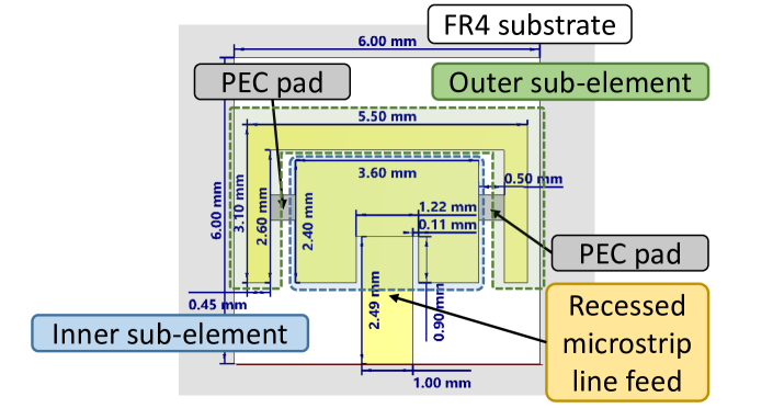
Our solution, namely FABRIS, complements the RIS optimization described above with an ad-hoc hardware design based on modular patch antennas capable of supporting multiple frequencies in a reconfigurable fashion. Specifically, since the main radiating frequency of an antenna depends on its physical geometry, we envision to divide each RIS element into two sub-elements, as shown in Fig. 1. By activating only the inner sub-element, the RIS operates at GHz while working at GHz when both sub-elements are active.
Frequency-agnostic operation. The electrical link between the sub-elements is a positive-intrinsic-negative (PIN) diode, which under zero- or reverse-bias (off state) attenuates most of the RF signal, thus isolating the two sub-elements, while behaving as a good RF conductor under forward bias (on state). Moreover, PIN diodes are often employed in RF circuits due to their fast switching times (in the order of hundreds of nanoseconds), thereby allowing us to set the RIS working frequency at run-time with no service disruption. Although RIS design often borrows from antenna theory, RISs are intrinsically different from radiating antennas as they do not transmit locally generated RF signals but only reflect the incoming electromagnetic (EM) waves. Hence, setting off the PIN diode does not prevent the reflection of the incoming EM energy onto both sub-elements. Therefore, whenever the PIN diode is off, we envision to connect the outer sub-element to a load whose impedance is matched to the characteristic impedance of such sub-element. As a result, the EM power impinging on it is absorbed, thus eliminating unwanted reflections while operating the RIS at frequency .
In order to introduce variable yet discrete phase shifts at each RIS element, we employ a set of microstrip-lines, whose length is given by [13], where is the desired phase shift, is the velocity factor of the microstrip-line, is the speed of light in vacuum and is the working frequency. As the microstrip-line length depends on the selected frequency, two transmission lines are needed to provide a single phase shift at the two operating frequencies, i.e. and . Hence, the RIS controller makes use of two RF switches per RIS element, each of them dedicated to a single sub-element, to route the RF signal to a specific microstrip-line in light of the required phase shift on the reflected signal. Besides, the RF switch downstream of the outer sub-element has an additional port for the matched load to support full power absorption when operating the RIS at , i.e. with PIN diode off. It is worth highlighting that further engineering of the working frequencies may reduce the number of required transmission lines at the expense of a more complex switching network. For instance, if , with , the same transmission line introducing a phase shift at provides a phase shift at (net of phase wrapping around ).
| Parameter | Value | Parameter | Value |
| Dielectric thickness | mm | Dielectric material | FR-4 (lossy) |
| Antenna material | copper (annealed) | Antenna thickness | mm |
Full-wave simulation. Let us validate our RIS design by means of full-wave simulations in CST Studio Suite 2021 [14]. The geometry of a single RIS element is shown in Fig. 1, wherein the circuital behavior of the connecting PIN diode is modeled by means of PEC pads [15]. In particular, when the diode is ON, the sub-elements are physically connected through two PEC pads, whereas no pad is used with the diode in the off state. The physical dimensions of the PEC pads reflect the typical size of a PIN diode, see e.g. [16]. Moreover, the patch antenna is matched using a recessed microstrip-line feed while we make use of National Electrical Manufacturers Association (NEMA) FR4 as substrate material. The design and simulation parameters are listed in Table I.
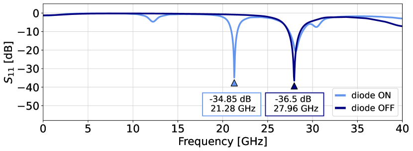
RIS element validation. First, we feed a single RIS element with a transmission line and evaluate its [13] when working either at or , namely with diode off or with diode on, respectively. As shown in Fig. 2, the strongly dips at (diode off) and at (diode on), reaching its global minimum in both cases. Besides, although the obtained with diode on shows additional local minima, their values are considerably higher ( dB) than the global minimum at , thus confirming the effectiveness of our design.
RIS array response validation. We evaluate now the 2D array response of an RIS with elements, with unit cells given as in Fig. 1. Since it is not possible to reduce the effective inter-element distance, we set , where corresponds to the working frequency . Hence, when operating at , the ratio between the corresponding wavelength and the inter-element distance is lower than , thus resulting in mutual coupling among the elements. We would like to point out that by designing the inter-element distance based on , RIS operation at would likely result in a beampattern affected by grating lobes as the latter appear in array beampatterns whenever the inter-element distance is higher than a full working wavelength333Nonetheless, such design might be helpful in scenarios with sparse UE distributions to effectively support multicast communication..
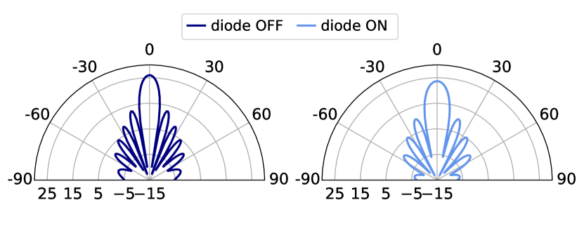
Fig. 3 shows the RIS beampattern obtained via CST full-wave simulations for the two different diode states. In particular, on the left-hand side the RIS is operated at frequency and exhibits a narrow beampattern thanks to the large number of available antennas and the inter-element distance of . Whereas, on the right-hand side the RIS is operated at frequency , which results in a ratio of inter-element spacing over wavelength of 0.42. The obtained beampattern is characterized by a comparable main lobe magnitude with respect to the previous case and, as expected, the side lobes and the beamwidth appear to be increased.
VI Numerical results
We present numerical results to validate our FABRIS design by examining the performance of the multi-frequency RIS described in Section V, which comprises of elements and is designed to have an inter-element distance of , with corresponding to the maximum supported working frequency of GHz. While such design behaves as a conventional RIS at the working frequency , in this section we focus on the effect of mutual coupling on the array response and the benefits of the procedure described in Section IV that aims at mitigating such unwanted effects. Hence, we set the working frequency to , with GHz, which corresponds to an inter-element spacing over wavelength ratio of .
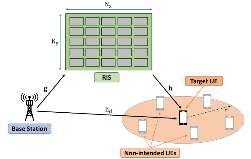
The considered scenario is depicted in Fig. 4, where the RIS is placed in position , whereas the UE is placed at . Furthermore, we set dBm and dBm. We assume that there are non-intended UEs uniformly distributed over a circle of (variable) radius around the target UE and we average our results over Monte Carlo independent realizations of their positions. We compare the performance of FABRIS against a naive approach where all the RIS elements are activated, with no concern for the effect in terms of mutual coupling on the resulting array response.
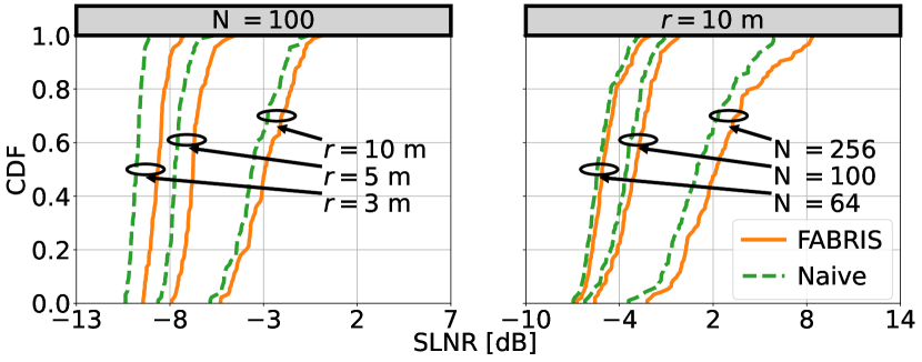
Fig. 5 shows on the left-hand side the CDF of the SLNR obtained with both the proposed FABRIS method and with the reference naive approach for different values of the radius over which the non-intended UEs are scattered. We notice that FABRIS effectively reduces leakage to neighbouring UEs by suitably optimizing the RIS activation profile as to mitigate the effects of mutual coupling, without excessively compromising beamforming gain, thus obtaining a sweet spot in the trade-off between the two. This effect is more evident for smaller values of , since the non-intended UEs may be very close to the target UE and thus experience strong leakage.
![[Uncaptioned image]](/html/2203.08633/assets/x6.png)
| Naive | FABRIS | |||
|
22.3 | 20.8 | ||
|
16.0 | 15.4 | ||
|
-10.8 | -7.7 |
The right-hand side of Fig. 5 shows the CDF of th SLNR for both considered approaches in the case of m and for different values of 444For simplicity, we assume to have a squared RIS, i.e., , although FABRIS may be readily applied to any rectangular RIS design.. Here, a lower value of leads to almost identical performances, since there are only few degrees of freedom to exploit in order to improve the directivity of the effective array response at the RIS. Whereas, for larger values of the proposed FABRIS method obtains highly-selective beamforming at a small cost in terms of beamforming gain at the target UE.
As an illustrative example, Fig. 6 shows the full-wave simulation in CST of the antenna array response at the RIS obtained with both the proposed FABRIS approach and with the reference naive method for a single realization in the case of and m. The proposed FABRIS approach reduces the main lobe angular width of at the expense of a small penalty in terms of main lobe magnitude. Besides, although the side lobe level (mainly provided by the beam pointing at ) appears to be increased by dB, the leakage level in the vicinity of the UE, i.e. in the directions within the circle of radius m centered around the UE, is greatly reduced, thereby improving the selected SLNR metric.
Lastly, we would like to remark that while in this paper we make a first attempt at designing a multi-frequency RIS, we expect much larger gains brought by the proposed FABRIS approach when moving from binary to higher-order and wider ranges of supported frequencies, which is left as future work.
VII Conclusions
In this paper, we presented FABRIS, a practical RIS design enabling operation at multiple frequencies. FABRIS builds upon a novel patch antenna layout involving two sub-elements connected via a PIN diode whose bias can be controlled to set the on or off states. The proposed hardware design is complemented by a novel optimization approach that outputs the RIS both the phase shifts configuration, which is obtained via microstrip-lines of different lengths, and the sub-elements activation profile as to reduce signal leakage in unwanted directions. Our results, involving synthetic and full-wave simulations, show that optimizing both variables leads to substantial performance gains with respect to a reference naive approach that does not consider the leakage generated by multi-frequency antenna arrays. Future work will consider the case of multiple antennas and both higher-order and wider ranges of supported operating frequencies.
References
- [1] M. Di Renzo, A. Zappone, M. Debbah, M.-S. Alouini, C. Yuen, J. de Rosny, and S. Tretyakov, “Smart Radio Environments Empowered by Reconfigurable Intelligent Surfaces: How It Works, State of Research, and The Road Ahead,” IEEE Journal on Selected Areas in Communications, vol. 38, no. 11, pp. 2450–2525, 2020.
- [2] L. Dai, M. D. Renzo, C. B. Chae, L. Hanzo, B. Wang, M. Wang, X. Yang, J. Tan, S. Bi, S. Xu, F. Yang, and Z. Chen, “Reconfigurable Intelligent Surface-Based Wireless Communications: Antenna Design, Prototyping, and Experimental Results,” IEEE Access, vol. 8, pp. 45 913–45 923, 2020.
- [3] P. Mursia, V. Sciancalepore, A. Garcia-Saavedra, L. Cottatellucci, X. Costa-Perez, and D. Gesbert, “RISMA: Reconfigurable Intelligent Surfaces Enabling Beamforming for IoT Massive Access,” IEEE Journal on Selected Areas in Communications, vol. 39, no. 4, pp. 1072–1085, 2021.
- [4] A. Albanese, V. Sciancalepore, and X. Costa-Pérez, “First Responders Got Wings: UAVs to the Rescue of Localization Operations in Beyond 5G Systems,” IEEE Communications Magazine, vol. 59, no. 11, pp. 28–34, 2021.
- [5] A. Albanese, F. Devoti, V. Sciancalepore, M. Di Renzo, and X. Costa-Pérez, “MARISA: A Self-configuring Metasurfaces Absorption and Reflection Solution Towards 6G,” in IEEE INFOCOM 2022 - IEEE Conference on Computer Communications, 2022.
- [6] E. Calvanese-Strinati, et al., “Reconfigurable, intelligent, and sustainable wireless environments for 6g smart connectivity,” IEEE Communications Magazine, vol. 59, no. 10, pp. 99–105, 2021.
- [7] G. C. Trichopoulos, P. Theofanopoulos, B. Kashyap, A. Shekhawat, A. Modi, T. Osman, S. Kumar, A. Sengar, A. Chang, and A. Alkhateeb, “Design and Evaluation of Reconfigurable Intelligent Surfaces in Real-World Environment,” 2021. [Online]. Available: http://arxiv.org/abs/2109.07763
- [8] J.-B. Gros, V. Popov, M. A. Odit, V. Lenets, and G. Lerosey, “A Reconfigurable Intelligent Surface at mmWave Based on a Binary Phase Tunable Metasurface,” IEEE Open Journal of the Communications Society, vol. 2, pp. 1055–1064, 2021.
- [9] Q. Wu, S. Zhang, B. Zheng, C. You, and R. Zhang, “Intelligent Reflecting Surface-Aided Wireless Communications: A Tutorial,” IEEE Transactions on Communications, vol. 69, no. 5, pp. 3313–3351, 2021.
- [10] M. Dunna, C. Zhang, D. Sievenpiper, and D. Bharadia, “ScatterMIMO: enabling virtual MIMO with smart surfaces,” in Proceedings of the 26th Annual International Conference on Mobile Computing and Networking (MOBICOM), 2020.
- [11] X. Pei, H. Yin, L. Tan, L. Cao, Z. Li, K. Wang, K. Zhang, and E. Björnson, “RIS-Aided Wireless Communications: Prototyping, Adaptive Beamforming, and Indoor/Outdoor Field Trials,” IEEE Transactions on Communications, vol. 69, no. 12, pp. 8627–8640, 2021.
- [12] N. Aftab, H. T. Chattha, Y. Jamal, A. Sharif, and Y. Huang, “Reconfigurable patch antenna for wireless applications,” in Proceedings of the 9th European Conference on Antennas and Propagation (EuCAP), 2015.
- [13] C. Balanis, Antenna Theory: Analysis and Design. Wiley, 2012.
- [14] Dassault Systèmes Simulia Corp., “CST Studio Suite 2021.” [Online]. Available: https://www.3ds.com/products-services/simulia/products/cst-studio-suite/
- [15] A. Kishk, Advancement in Microstrip Antennas with Recent Applications. IntechOpen, 2013.
- [16] PIN Diode Basics. Application Note., Skyworks Solutions, Inc., 2008. [Online]. Available: https://www.skyworksinc.com/-/media/SkyWorks/Documents/Products/1-100/200823A.pdf