Distributed On-Sensor Compute System for AR/VR Devices:
A Semi-Analytical Simulation Framework for Power Estimation
Abstract.
Augmented Reality/Virtual Reality (AR/VR) glasses are widely foreseen as the next generation computing platform. AR/VR glasses are a complex ”system of systems” which must satisfy stringent form factor, computing-, power- and thermal- requirements. In this paper, we will show that a novel distributed on-sensor compute architecture, coupled with new semiconductor technologies (such as dense 3D-IC interconnects and Spin-Transfer Torque Magneto Random Access Memory, STT-MRAM) and, most importantly, a full hardware-software co-optimization are the solutions to achieve attractive and socially acceptable AR/VR glasses. To this end, we developed a semi-analytical simulation framework to estimate the power consumption of novel AR/VR distributed on-sensor computing architectures. The model allows the optimization of the main technological features of the system modules, as well as the computer-vision algorithm partition strategy across the distributed compute architecture. We show that, in the case of the compute-intensive machine learning based Hand Tracking algorithm, the distributed on-sensor compute architecture can reduce the system power consumption compared to a centralized system, with the additional benefits in terms of latency and privacy.
1. Introduction
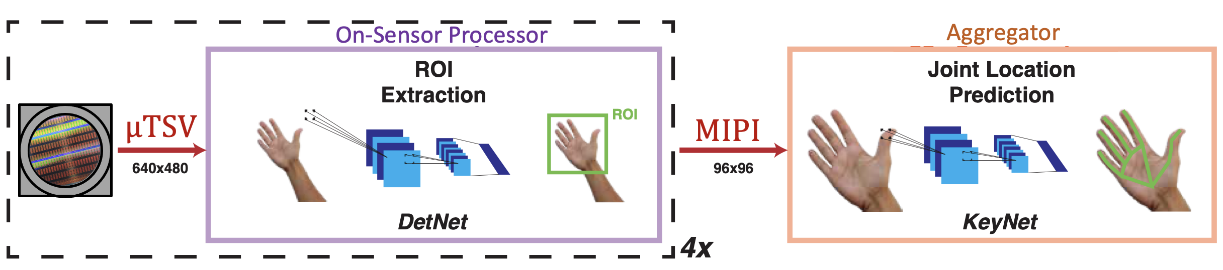
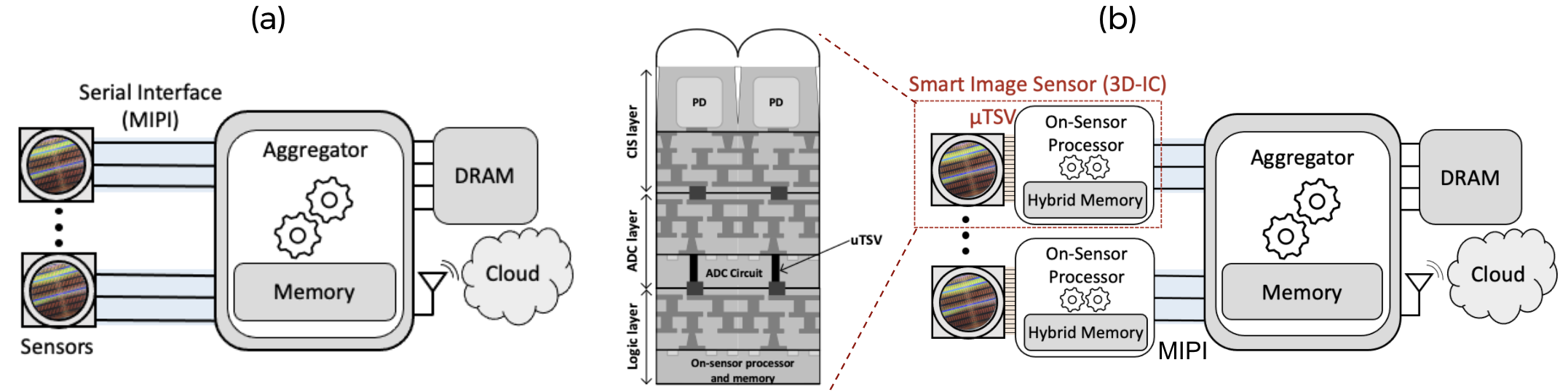
Mixed Reality, consisting of Virtual Reality (VR) and Augmented Reality (AR) together, will be the next general computing platform, dominating our relationship with the digital world for the next fifty years, much as personal computing has dominated the last fifty (Abrash, 2021). AI (Artificial Intelligence) processing is critical for AR/VR glasses, both for input (e.g., camera images, audio) and output (e.g., graphics rendering) (Li et al., 2021). Moreover, the AR/VR glasses has to deliver a responsive, low latency experience while consuming very limited power, both for battery life and to limit temperature rise on the skin for user comfort. At the system level, a large quantity of data is generated and must be processed in real time to support precise and low latency interaction between the physical world and the virtual world. In traditional AR/VR systems, the processing of the raw input data captured by several image sensors is performed in a central off-sensor edge-processor (named aggregator in Fig. 1 (a)). The new distributed on-sensor compute architecture (shown in Fig. 1 (b)) (Liu et al., 2022; Abrash, 2021; Liu et al., 2020) exploits multiple levels of computing, including on-sensor processors (for initial feature extraction and first level of processing) and a nearby aggregator for further processing and final analysis. The distributed compute system allows for minimum data movement with rapid and localized inference on the sensors, where a shallow portion of each Computer-Vision Neural Network (CV NN) model is implemented. This results in significant benefits in terms of communication costs, latency constraints and privacy concerns compared to centralized computing systems. On the other hand, several challenges need to be solved to implement an on-sensor processing units capable of tackling real-time compute/memory intensive workloads in the very small footprint and low power budget of AR/VR image sensors. As illustrated in Fig. 1 (b), innovative 3D CMOS Image Sensor (CIS) architectures will permit further shrinking of the sensor footprint and introduction of key on-sensor AI functionalities. Complex three-layer wafer stacking technologies are a promising solution for intelligent image sensor fabrication with AI capabilities. Dense and tight 3D-IC technologies, such as micro-Trough Silicon Vias () and wafer-level hybrid bonding, will enable heterogeneous monolithic integration of camera and processor. There is a clear need for integrating advanced logic as close to the sensors as possible. Moreover, use of hybrid memory hierarchy (including both SRAM and STT-MRAM) in the on-sensor computing architecture will allow for higher density and lower power. To quantify the trade-offs of Distributed On-Sensor Compute (DOSC) architectures for AR/VR workloads, a system simulation framework is required. Several accelerator simulation frameworks have been developed in recent years (Binkert et al., 2011; Parashar et al., 2019; Pinkham et al., 2021), mostly focused on the compute modules of the system. In this work, we propose a new semi-analytical model that captures the key technological features of the whole system hardware resources, including cameras, communication links, processors, and memories. Technological parameters used in the simulations for all modules are silicon-based. The compute and memory parameters of the system have been calibrated by using an event-based silicon-calibrated simulator (GVSoC (Burrello et al., 2021; Greenwaves Technologies, 2021)). Finally, for the system modeling demonstration, we focus on a common AR/VR workload: the Hand Tracking algorithm (Han et al., 2020) (see Fig. 2). In the case of a centralized compute system the complete image captured by the cameras is transmitted from the sensors to the aggregator through the MIPI and the full Hand Tracking workload is deployed on the aggregator. On the other hand, on a hierarchical compute system, an optimal repartition of the workload between the on-sensor processor and the aggregator is possible. In the distributed on-sensor compute system, the complete raw image is transmitted from the cameras to the on-sensor processors through the low-energy and high bandwidth interconnects. The region of interest (ROI) is thus computed on sensor, and only this data is transferred from the sensors to the aggregator through the energy-hungry MIPI interfaces. As detailed in (Han et al., 2020), the system uses four monochrome cameras. By means of our semi-analytical modeling, we will show that this optimal algorithm repartition across the novel distributed on-sensor compute architecture, as well as the introduction of new emerging technologies, allow for a significant improvement of the overall system power consumption.
2. Semi-Analytical System Modeling
In order to evaluate the energy efficiency of the distributed on-sensor computing system (Fig 1.(b)), we consider separately the system key modules, such as: cameras, communication links, on sensor processor and the corresponding on-sensor memory hierarchy, as well as aggregator processor and its memory hierarchy. We assume that the total energy per frame of the compute system is simply the addition of the energies of each module, i.e.:
| (1) |
where , , , and are the total camera, communication, compute, read, write, and leakage energy per frame (as calculated in eq.3, eq.5, eq.7, eq.8 and eq.11 respectively) for each camera (h), communication link (i), compute processor (j) and memory instance (k) present in the system. To calculate the average power (), we simply multiply by the fps at which each module operates, which gives:
| (2) |
For each module, we investigate the critical parameters that define its energetic behaviour and we derive simple analytical expressions to capture this behavior (as explained in the following subsections). Once we fix the AR/VR workload, the key parameters of the on-sensor and aggregator processor behavior and optimal dataflow across the multi-level memory hierarchy were extracted by means of the GVSoC tool (a light-weight, event-based instruction set simulator (Greenwaves Technologies, 2021)) and DORY (Burrello et al., 2021), respectively.
2.1. Digital Pixel Sensor
| Camera | Operation State | Power (mW) |
| Sensing | 15 | |
| DPS | Read Out | 36 |
| Idle | 1.5 |
We consider the image sensors of the distributed on-sensor compute system being based on a AR/VR custom digital pixel sensor (DPS) technology (detailed elsewhere (Liu et al., 2020)). The camera analytical model assumes that the sensing and readout energy are proportional to the sensing time, , and the readout time, , respectively. The sensing time includes the exposure and the analog to digital converter (ADC) times. We calculate the energy of the camera as follows:
| (3) |
where , and are the sensing, read out and off power respectively (Table 1). The sensing time is the sum of the exposure and ADC time (). is the read-out time (see later Eq. 6) that depends on the interface between the camera and the compute module. Finally, is the rest of the time which can be simply calculated as follows:
| (4) |
2.2. Communication Links
Different interfaces are used in the DOSC architecture, as shown in Fig. 1 (b), in particular: between the image sensor and the on-sensor compute layer, and MIPI between the on-sensor processor and the aggregator. Each interface is characterized by the energy it requires to transmit a Byte of information () and by its bandwidth (). The total energy of the communication link () is given by the following equation:
| (5) |
where is the size of the data (in Bytes) transmitted trough the interface, which depends on the workload. As shown in Fig. 2, can correspond to the raw image (transferred from the camera to the on-sensor processing layer), the Region of Interest (ROI) from the input image, or it could be the Neural Network activation map output (transferred from the on-sensor processing unit to the aggregator). The communication time () is then equal to:
| (6) |
The energy and bandwidth values corresponding to the two interfaces and MIPI used in our distributed system are given in Table 2 (based on literature data).
2.3. On-Sensor and Aggregator AI Processors and Memories
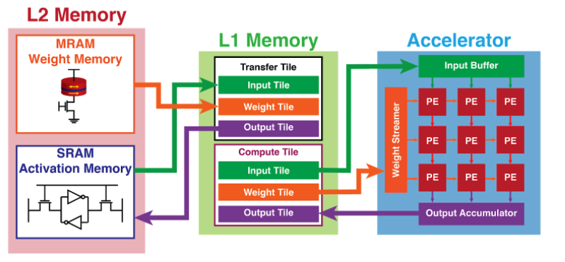
The computing architecture used for the on-sensor processing and aggregator is based on the PULP computing platform (Pullini et al., 2019; Greenwaves Technologies, 2021; Valente et al., 2021). In this work, we assume that the AR/VR workload computation is completely done in the DNN hardware accelerator, a Reconfigurable Binary Engine (RBE) (Conti et al., 2018). The RBE has a maximum throughput of 133 MAC/Cycle, running on 8-bit precision weights and activations. As shown in Fig. 3, the simulated memory hierarchy includes two levels: a small Level 1 memory and two larger Level 2 memories (activation memory and weight memory). We separate L2 activation from L2 weight memory, in order to explore the impact of using STT-MRAM as L2 weight memory.
In our semi-analytical model, the compute energy per frame is given by:
| (7) |
where is the total number of Multiply Accumulate (MAC) operations for processing one frame and is the energy per MAC operation, depending on the specific technology node.
The access energy for the different memory levels (L1 or L2) is then computed as follows:
| (8) |
where is the total number of read or write (for an specific memory level) and is the read or write energy per byte (for the specific memory level and the specific technology node).
To calculate the impact of the memory leakage, we first need to calculate the amount of time that the memory is in On-state, in Retention-state, or Off-state. To this scope, we use the following equation:
| (9) |
where is the number of MACs of layer j, is the throughput that the system has at layer j and is the clock frequency. The processing time is the time that the memory will be in On-state. The rest of the time the memory can be in Retention- or Off-state, depending on the memory type. We can simply calculate the idle time by using the following equation:
| (10) |
Finally, the total memory leakage energy per frame for each memory level will be given by the following equation:
| (11) |
where and are the leakage power in On, Retention or Off state respectively, depending on the specific technology.
The energy and power values used in simulations for the elementary MAC operation and the memory read/write access or leakage (i.e. , , and ) are extracted from post-synthesis simulations and memory compilers, respectively. In this work, we used 7nm and 16nm logic process nodes and libraries from leading foundries. STT-MRAM values correspond to values from test-vehicles fabricated in 16nm logic technology (Guedj, 2021).
On the other hand, the number of operations, the processing efficiency, the memory operations counts and accelerator performance (, , , and ) are obtained by using the GVSoC/Dory/Nemo toolchain (Burrello et al., 2021; Greenwaves Technologies, 2021) to simulate the deployment of our AR/VR workload on the computing platforms. GVSoC allows us to capture the processing performance depending on the layer configuration and the arithmetic intensity of the NN layer (on each memory level). This is especially important when complex memory hierarchies are considered with different capacities, bandwidths and non-symmetric read-write performances. To deploy the workload across the different memory levels, we modified DORY tiling engine (Burrello et al., 2021) to work with the RBE accelerator.
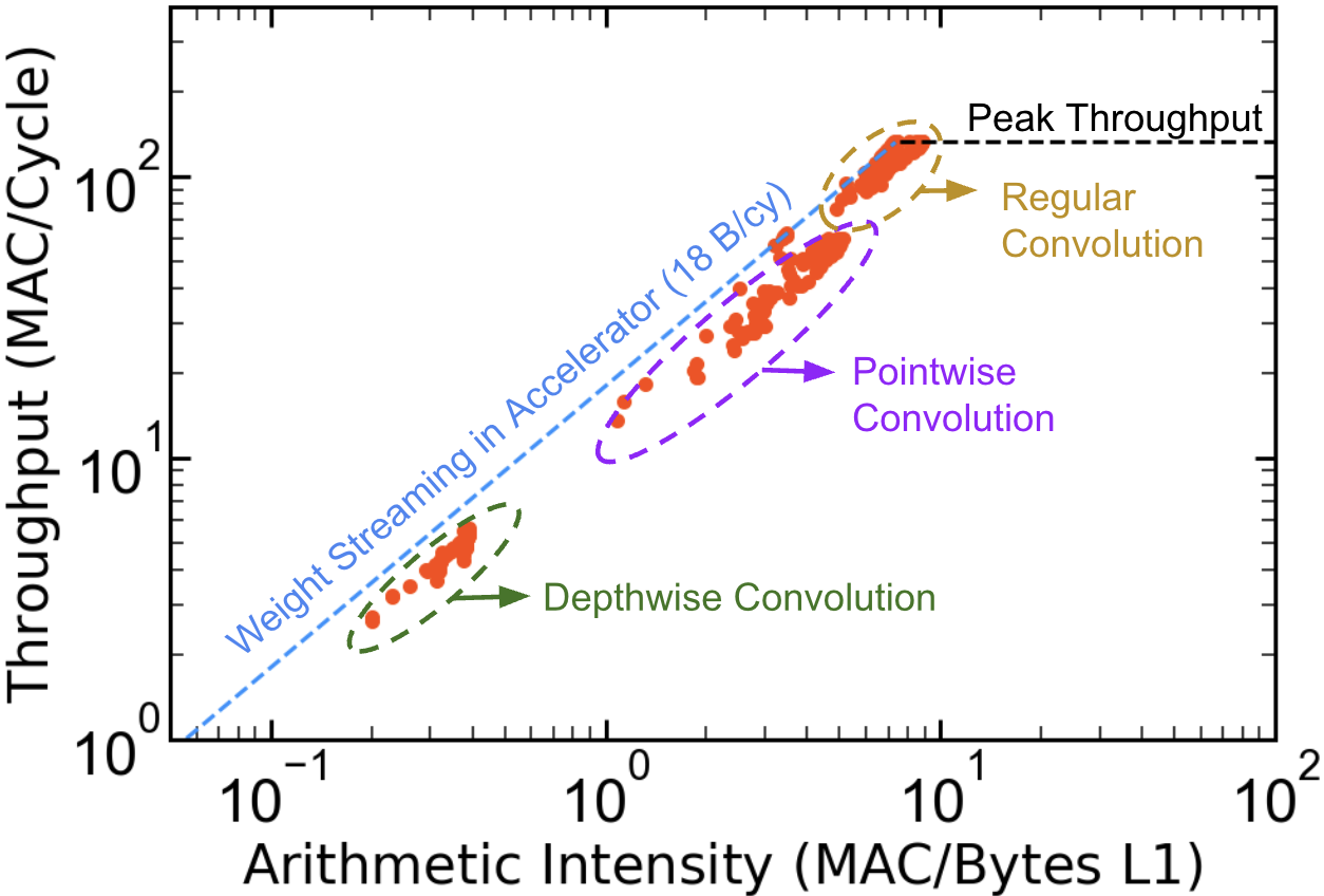
Using GVSoC we also characterized several representative layers of our workloads that include among others Regular, Depthwise separable, and Pointwise convolutions with varying channel dimension and spatial fields. Using these simulations we obtained the roofline plot for the RBE accelerator shown in Fig 4. The roofline plot allows us to understand the accelerator performance in relation to memory bandwidth constraints. From the plot, we can see that layer performance is almost completely bounded by the weight streaming in the accelerator. The RBE demonstrates close to peak performance on full convolutional benchmarks, with diminishing performance for pointwise kernels, and even further decrease when doing depthwise kernels. We note that the RBE has been designed and optimized for a particular architecture, memory bandwidth, and set of workloads. Because of this, the architecture is most efficient for certain network types as compared to others, as shown by the high throughput of convolution kernels compared to pointwise and depthwise kernels.
Now that we have all the blocks to calculate the system energy per frame and the average power, we will use our semi-analytical simulation model to explore the Hand Tracking workload.
3. Distributed On-Sensor System Simulations for Hand-Tracking
The semi-analytical model was used to compare the energy efficiency of the DOSC system versus a traditional centralized compute system, while deploying a Hand-Tracking (HT) workload for AR/VR experience. As mentioned previously, the HT NN consists in two consecutive Machine Learning algorithms (Fig. 2). The first ML model (DetNet) is used to define the region of interest (ROI), while the second model (KeyNet) is used to detect the joint locations and hand pose. Note that the two ML models, on sensor and in the aggregator, can run at different frames-per-second giving us an additional knob for power optimization. As suggested to improve energy efficiency in (Han et al., 2020), the DetNet model is not run at every frame as the same ROI can be used for multiple frames. In our simulations, we assume that the on-sensor compute capability and corresponding memory size to be one fourth of the aggregators. The L2 weight memories were sized to hold the full weights of the models. The weight memories’ operations are mainly read-dominated. On the contrary, the activation memories need to support both read and write operations during the inference. This network has many features which help demonstrate it as a representative workload for our applications. Namely, it is a common and necessary AR/VR application, it has a natural partition point to demonstrate how computation can be split between on-sensor and off-sensor, and it is sufficiently computationally intensive to strain many current systems.
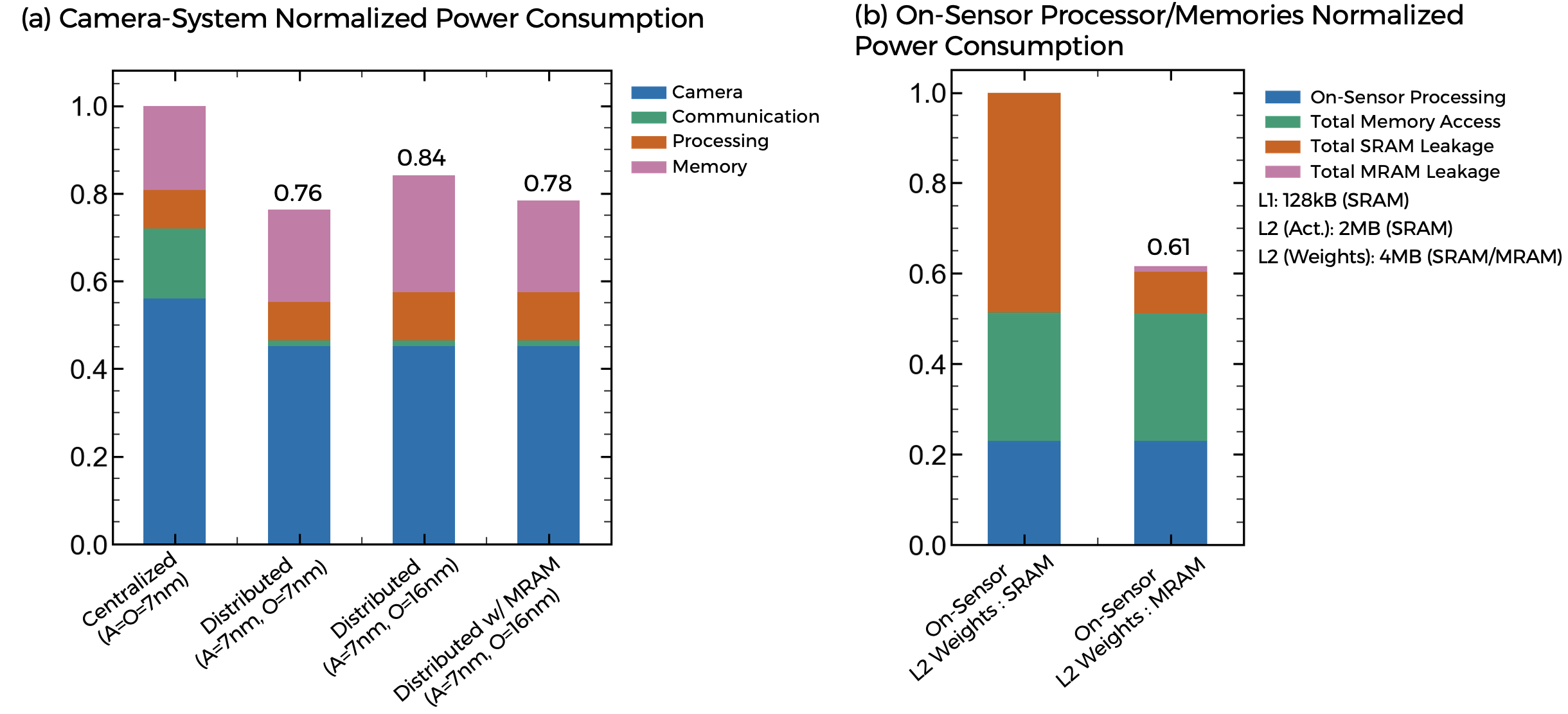
As shown in Fig. 5, our simulation results demonstrate that the cameras and MIPIs dominate the power dissipation of the centralized compute system. On the other hand, when we migrate from a centralized to a distributed system, results show a significant system power reduction (24%, as shown in Fig. 5 (a)). Even when the on-sensor processor technology node is less advanced than the aggregator’s (16nm rather than 7nm), there is still a significant power reduction (16%). The power gain is mainly due to the decreased usage of the energy-hungry serial interface (MIPI) thanks to the on-sensor processing and subsequent feature compression. Additionally, the image sensor power is also reduced. This is because the wider data bandwidth of the interconnects (between the camera and the on-sensor processor) compared to MIPI allows us to reduce the sensor digital data read-out time and consequently to extend the sensor low-power standby mode. However, it also appears that the total memory energy consumption slightly increases in the distributed computing system due to the duplication of the weight storage memory in each sensor, increasing the total memory size of the system and thus the leakage energy contribution. Finally, Fig. 5 (b) shows that a hybrid on-sensor memory architecture (STT-MRAM for weight storage and SRAM for activation) could reduce the overall on-sensor power consumption by 39% thanks to STT-MRAM’s negligible leakage. Moreover, the use of STT-MRAM also allows us to improve the overall on-sensor memory’s form factor, as STT-MRAM features approximately 2x higher memory density than SRAM (Guedj, 2021).
4. Conclusion
In this paper, we proposed a semi-analytical simulation framework suitable for optimization of AR/VR distributed on-sensor computing architectures. This model allowed us to study simultaneously the impact of the main technological features of the system modules (cameras, interfaces, accelerators, memories) on the overall system power consumption, as well as the impact of the partitioning of the deployed AR/VR CV NNs across the different resources. When an AR/VR Hand Tracking optimized workload is partitioned over the distributed system, the model predicts significant power savings compared to traditional centralized systems, thanks to:
-
(1)
Improved communication power, as only high-level data representation is transferred from the sensors to the aggregator through the energy hungry MIPI interfaces, while the first level of processing is performed on sensor.
-
(2)
Reduced camera read-out time (and consequently reduced camera power consumption), thanks to monolithic integration of camera and on-sensor processor through high bandwidth/low energy interconnects
-
(3)
Use of STT-MRAM as L2 weight memory on sensor, allowing for 2x higher memory density (thus smaller area) and improved power consumption, thanks to the negligible leakage of STT-MRAM compared to SRAM.
Finally, a significant reduction in the system power remains when the on-sensor processor is implemented in an older technology node than the aggregator’s. However, the older technology node will penalize the on-sensor processor form factor.
Acknowledgements.
The authors would like to thank Francesco Conti, Davide Rossi, Alessio Burrello, Nazareno Bruschi, Arpan Prasad, Luca Benini of the Integrated Systems Laboratory (IIS) of ETH Zürich for their valuable advice and support with the DORY/NEMO compilation tool chain and computing system architecture definition.References
- (1)
- Abrash (2021) Michael Abrash. 2021. Creating the Future: Augmented Reality, the next Human-Machine Interface. International Electron Devices Meeting, IEDM 2021-Decem (2021).
- Binkert et al. (2011) Nathan Binkert, Bradford Beckmann, Gabriel Black, Steven K. Reinhardt, Ali Saidi, Arkaprava Basu, Joel Hestness, Derek R. Hower, Tushar Krishna, Somayeh Sardashti, Rathijit Sen, Korey Sewell, Muhammad Shoaib, Nilay Vaish, Mark D. Hill, and David A. Wood. 2011. The gem5 simulator. ACM SIGARCH Computer Architecture News 39, 2 (may 2011), 1–7. https://doi.org/10.1145/2024716.2024718
- Burrello et al. (2021) Alessio Burrello, Angelo Garofalo, Nazareno Bruschi, Giuseppe Tagliavini, Davide Rossi, and Francesco Conti. 2021. DORY: Automatic End-To-End Deployment of Real-World DNNs on Low-Cost IoT MCUs. IEEE Trans. Comput. 70, 8 (2021), 1253–1268. https://doi.org/10.1109/TC.2021.3066883 arXiv:2008.07127
- Choi et al. (2021) Seokwon Choi, Changmin Song, and Young-Chan Jang. 2021. A 3.0 Gsymbol/s/lane MIPI C-PHY Receiver with Adaptive Level-Dependent Equalizer for Mobile CMOS Image Sensor. Sensors 21, 15 (2021). https://doi.org/10.3390/s21155197
- Conti et al. (2018) Francesco Conti, Pasquale Davide Schiavone, and Luca Benini. 2018. XNOR Neural Engine: A Hardware Accelerator IP for 21.6-fJ/op Binary Neural Network Inference. IEEE Transactions on Computer-Aided Design of Integrated Circuits and Systems 37, 11 (Nov 2018), 2940–2951. https://doi.org/10.1109/tcad.2018.2857019
- Greenwaves Technologies (2021) Greenwaves Technologies. 2021. GVSOC - The Full System Simulator for profiling GAP Applications. https://greenwaves-technologies.com/gvsoc-the-full-system-simulator-for-profiling-gap-applications/
- Guedj (2021) Jack Guedj. 2021. A 2MB, 16nm, sub 5ns Reads, MRAM-based Memory IP Core. 12th MRAM Global Innovation Forum 2021-April (2021).
- Han et al. (2020) Shangchen Han, Beibei Liu, Randi Cabezas, Christopher D. Twigg, Peizhao Zhang, Jeff Petkau, Tsz Ho Yu, Chun Jung Tai, Muzaffer Akbay, Zheng Wang, Asaf Nitzan, Gang Dong, Yuting Ye, Lingling Tao, Chengde Wan, and Robert Wang. 2020. MEgATrack: Monochrome Egocentric Articulated Hand-Tracking for Virtual Reality. ACM Transactions on Graphics 39, 4 (jul 2020). https://doi.org/10.1145/3386569.3392452
- Li et al. (2021) Tianye Li, Mira Slavcheva, Michael Zollhöfer, Simon Green, Christoph Lassner, Changil Kim, Tanner Schmidt, Steven Lovegrove, Michael Goesele, and Zhaoyang Lv. 2021. Neural 3D Video Synthesis. CoRR abs/2103.02597 (2021). arXiv:2103.02597 https://arxiv.org/abs/2103.02597
- Liu et al. (2020) Chiao Liu, Lyle Bainbridge, Andrew Berkovich, Song Chen, Wei Gao, Tsung Hsun Tsai, Kazuya Mori, Rimon Ikeno, Masayuki Uno, Toshiyuki Isozaki, Yu Lin Tsai, Isao Takayanagi, and Junichi Nakamura. 2020. A 4.6m, 512×512, ultra-low power stacked digital pixel sensor with triple quantization and 127dB dynamic range. Technical Digest - International Electron Devices Meeting, IEDM 2020-Decem (2020), 16.1.1–16.1.4. https://doi.org/10.1109/IEDM13553.2020.9371913
- Liu et al. (2022) Chiao Liu, Song Chen, Tsung-Hsu Tsai, Barbara De Salvo, and Jorge Gomez. 2022. Augmented Reality — the Next Frontier of Image Sensors and Compute Systems. International Solid-State Circuits Conference, ISSCC 2022-Feb (2022).
- Parashar et al. (2019) Angshuman Parashar, Priyanka Raina, Yakun Sophia Shao, Yu Hsin Chen, Victor A. Ying, Anurag Mukkara, Rangharajan Venkatesan, Brucek Khailany, Stephen W. Keckler, and Joel Emer. 2019. Timeloop: A Systematic Approach to DNN Accelerator Evaluation. Proceedings - 2019 IEEE International Symposium on Performance Analysis of Systems and Software, ISPASS 2019 (apr 2019), 304–315. https://doi.org/10.1109/ISPASS.2019.00042
- Pinkham et al. (2021) Reid Pinkham, Andrew Berkovich, and Zhengya Zhang. 2021. Near-Sensor Distributed DNN Processing for Augmented and Virtual Reality. IEEE Journal on Emerging and Selected Topics in Circuits and Systems (oct 2021), 1–1. https://doi.org/10.1109/JETCAS.2021.3121259
- Pullini et al. (2019) Antonio Pullini, Davide Rossi, Igor Loi, Giuseppe Tagliavini, and Luca Benini. 2019. Mr.Wolf: An Energy-Precision Scalable Parallel Ultra Low Power SoC for IoT Edge Processing. IEEE Journal of Solid-State Circuits 54, 7 (2019), 1970–1981. https://doi.org/10.1109/JSSC.2019.2912307
- Takla and Lee (2017) Ashraf Takla and C.K. Lee. 2017. MIPI C-PHYSM/D-PHYSM Dual Mode Subsystem Performance & Use Cases. MIPI Alliance Developers Conference, DEVCON (2017).
- Valente et al. (2021) Luca Valente, Davide Rossi, and Luca Benini. 2021. Hardware-In-The Loop Emulation for Agile Co-Design of Parallel Ultra-Low Power IoT Processors. 2021 IFIP/IEEE 29th International Conference on Very Large Scale Integration (VLSI-SoC) (oct 2021), 1–6. https://doi.org/10.1109/vlsi-soc53125.2021.9607006
- Vivet et al. (2020) Pascal Vivet, Eric Guthmuller, Yvain Thonnart, Gael Pillonnet, Guillaume Moritz, Ivan Miro-Panadès, Cesar Fuguet, Jean Durupt, Christian Bernard, Didier Varreau, Julian Pontes, Sebastien Thuries, David Coriat, Michel Harrand, Denis Dutoit, Didier Lattard, Lucile Arnaud, Jean Charbonnier, Perceval Coudrain, Arnaud Garnier, Frederic Berger, Alain Gueugnot, Alain Greiner, Quentin Meunier, Alexis Farcy, Alexandre Arriordaz, Severine Cheramy, and Fabien Clermidy. 2020. 2.3 A 220GOPS 96-Core Processor with 6 Chiplets 3D-Stacked on an Active Interposer Offering 0.6ns/mm Latency, 3Tb/s/mm¡sup¿2¡/sup¿ Inter-Chiplet Interconnects and 156mW/mm¡sup¿2¡/sup¿@ 82%-Peak-Efficiency DC-DC Converters. In 2020 IEEE International Solid- State Circuits Conference - (ISSCC). 46–48. https://doi.org/10.1109/ISSCC19947.2020.9062927