Ultra-sharp lateral junctions in modulation-doped graphene
Abstract
We demonstrate ultra-sharp () lateral junctions in graphene using electronic transport, scanning tunneling microscopy, and first principles calculations. The junction lies at the boundary between differentially-doped regions of a graphene sheet, where one side is intrinsic and the other is charge-doped by proximity to a flake of -RuCl3 across a thin insulating barrier. We extract the junction contribution to the device resistance to place bounds on the junction width. We achieve an ultra-sharp junction when the boundary between the intrinsic and doped regions is defined by a cleaved crystalline edge of -RuCl3 located 2 nm from the graphene. Scanning tunneling spectroscopy in heterostructures of graphene, hexagonal boron nitride, and -RuCl3 shows potential variations on a sub-10 nm length scale. First principles calculations reveal the charge-doping of graphene decays sharply over just nanometers from the edge of the -RuCl3 flake.
keywords:
Graphene, -RuCl3, junction, electronic transport, scanning tunneling microscopy, density functional theoryIdeal junctions in graphene with a step-function change in carrier density underlie the physics of Klein tunneling 1, 2, 3, 4, negative refraction required for Veselago lensing 5, 6, guiding of plasmons 7 and snake states 8. Such junctions may also enable controlled anisotropy of the band velocity 9, 10, novel electron-optical devices based on transformation optics 11, or the ability to focus electron beams 12, 13, 14, 15. In practice, junctions defined by electrostatic gating are far from this ideal, with the change in carrier density taking place over due to fringe electric fields from the edges of the metallic gates 16, 6, 17, precluding observation of effects such as Veselago lensing that rely on sub-10-nm junctions6. Here we employ modulation-doping of graphene by close () proximity to -RuCl3 18, and a well-defined boundary to the doped region via a cleaved edge of the -RuCl3 flake, to create ultra-sharp junctions, demonstrated with evidence from electronic transport, scanning tunneling probes, and first principles calculations.
When the layered Mott insulator alpha-ruthenium(III) chloride (-RuCl3) is placed in direct contact with graphene, it accepts approximately electrons, leaving the graphene strongly hole-doped 19, 20, 21, 22, 23. If an insulating spacer is introduced between the two materials, the charge transfer is weakened and the mobility increases commensurate with the setback of -RuCl3 from graphene, analogous to modulation doping of conventional two-dimensional electron gases18, 24. The spatial distribution of the hole-doping is determined by where the -RuCl3 overlaps the graphene which can in principle have an atomically-abrupt boundary. Thus charge-doping by -RuCl3 appears to be a viable route toward ultra-sharp junctions in graphene.
Here we fabricate - junctions in graphene by a combination of modulation-doping to differentially charge-dope two regions, and electrostatic gating to independently tune the densities in each. We use the resistance measured across the junctions to extract the junction width and find an ultra-sharp, junction when a cleaved crystalline edge of the dopant -RuCl3 flake placed 2 nm away from the graphene defines the boundary between the regions. We further use low-temperature scanning tunneling microscopy and spectroscopy (STM/STS) to explore devices where a graphene sheet is either directly in contact with -RuCl3 or separated from it by thin flakes of hexagonal boron nitride (hBN). We observe a sharp change in the charge doping of the graphene over a sub- length scale across step edges in the insulating hBN spacer. Finally, we perform density functional theory (DFT) calculations that reveal the hole-doping of graphene due to electron transfer to -RuCl3 falls off rapidly over just a few graphene lattice constants from the -RuCl3 edge.
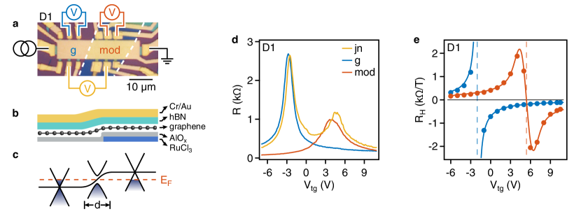
We present electronic transport in two graphene devices containing lateral junctions. In both, half the graphene sheet is intrinsic while the other half is modulation-doped by an -RuCl3 flake. Device D1 has a -nm-thick AlOx film between the graphene and -RuCl3, while device D2 has a 2-nm-thick flake of hBN as a spacer. Figure 1a shows an optical microscope image of D1, which consists of a 16.5-nm-thick flake of -RuCl3 coated by the AlOx film, topped by a graphene Hall bar that lies partly above the -RuCl3 and partly on the bare substrate. The Hall bar is capped by a flake of hBN () supporting a global Cr/Au top gate, and is contacted by Cr/Au leads. The entire device rests on of SiO2 on -Si; the latter also serves as a global back gate. Further fabrication details are given in the Supporting Information 25. In Fig. 1a, the device regions labeled “g” and “mod” correspond to the intrinsic and -RuCl3-doped graphene, respectively, and a profile of the device stack is shown schematically in Fig. 1b.
Four-terminal resistance measurements at K of the g and mod side of device D1 are shown in Fig. 1d, as a function of the top gate voltage. On either side of the junction we see resistance maxima at the graphene charge neutrality point (CNP or Dirac point), shifted by a few volts relative to each other due to the -type modulation-doping 19, 20, 26. Measurements of the low-field Hall coefficient, , shown in Fig. 1e directly show the charge-doping difference to be . Similarly, in the hBN-spaced device D2, the charge transfer is 25. Typical g-side (mod-side) mobilities and mean free paths in D1 range from and ( and ) 25. Intriguingly, although the top and back gates are global, the carrier densities on either side can be independently tuned. Thus the back-gate electric field on the modulation-doped side must be screened by the -RuCl325.
The width of a graphene junction can be determined by its contribution to the total device resistance. Charge carriers incident on a junction in graphene obey an electronic analog of Snell’s law at an interface of right- and left-handed optical materials: the momentum along the junction, , is conserved, but the momentum normal to the junction changes sign, the end result being a negative refraction 28, 29. Here is the Fermi momentum and is the carrier angle of incidence on the junction. Carriers are transmitted across an abrupt junction with probability due to pseudospin conservation. In real devices there is always a density gradient from - to -type over some characteristic width , analogous to the depletion region of a classical doped-Si junction. Although there is no band gap in graphene, an effective gap to transmission arises when becomes imaginary, where is the position-dependent energy of the graphene Dirac point across the junction, and m/s is the Fermi velocity. This is depicted schematically in Fig. 1c. Tunneling across this gap reduces the transmission probability as a function of impact angle and junction width which, for a balanced junction (), is given by 28
| (1) |
The reduced transmission leads to a finite resistance that has both ballistic and diffusive contributions, , whose relative magnitudes depend on the carrier mean free path and also many-body effects 30, 31, 25. Experimental values of range from a few hundred ohms in graphene-on-oxide junctions to 100 in hBN-encapsulated junctions 32, 2, 6.
We extract the width of lateral junctions in two devices as follows, illustrating the procedure by analyzing the transport in device D1. First, in Fig. 2a we show the top- and back-gate dependence of the total resistance across the junction, , using the contacts marked in yellow in Fig. 1a for D1. This quantity includes the sheet resistances from both sides of the junction, and due to the junction itself. The density of the intrinsic portion of the graphene depends on both gates as , while the -RuCl3-doped portion depends only on the top gate via . Here the top and back gating efficiencies are /V and /V, respectively, and the densities for zero applied gate bias are and . Using these relations, in Fig. 2b we re-plot vs the carrier densities of the intrinsic graphene, , and the modulation-doped graphene, . The CNPs of these two differentially-doped regions appear as vertical and horizontal bands separating the regimes of same-sign (- or -) carrier transport across the interface from those having bipolar transport.
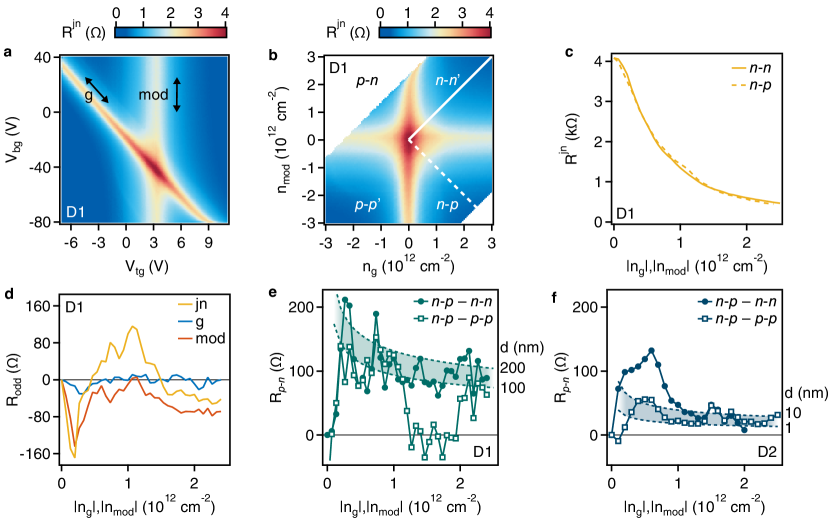
Next we isolate the resistance, , of the junction itself. We start with line cuts of along lines of equal carrier density and same sign (, yielding ) or opposite sign (, ). These are plotted together in Fig. 2c. To the extent that sheet resistances on either side of the interface are symmetric with respect to charge neutrality, then the difference of these curves, , will be due only to the resistance of the junction: . In fact, for the line cuts in Fig. 2c the contribution from the g-side sheet resistance ought to be identical because the g-side carrier density does not change sign. In contrast, the two line cuts include either - or -type doping of the mod side, so any asymmetry about the CNP in this region will add an additional resistance to that must be subtracted off. To determine the presence of this additional contribution, we make resistance maps analogous to Fig. 2b for both the g and mod side 25. From equivalent line cuts along the and directions, we calculate and . These, along with , are shown in Fig. 2d. As expected, lies close to zero; but and are finite and share a similar lineshape.
It remains to subtract this asymmetric part of the sheet resistance to finally obtain the junction resistance: , where are scaling factors appropriate to the device geometry 25. Figure 2e shows the resulting values, along with the analysis for line cuts along the and directions which should in principle yield the same junction resistance. Indeed, both show values of (but for a brief excursion by the -derived trace which can be attributed to a dip in 25). Figure 2f shows the results of similar analyses carried out in device D2. Here, both curves show peaks at low density that rapidly converge to values between 20 and 30 over much of the carrier density range. We compare these results to theoretical predictions for the resistance of junctions in disordered graphene 31, which we plot as shaded bands calculated for junction widths that span 100 to 200 nm and 1 to 10 nm in Fig. 2e and f, respectively. Device D2 is thus found to have an ultra-sharp, sub-10-nm junction, while D1 has a much wider junction.
At first, this result is surprising: why are the two junction widths so different? Both have insulating spacers of approximately the same thickness, with modulation-doping levels only a factor of two apart. The differing mobilities are unlikely to be the culprit, as transport across the junction is firmly in the ballistic regime25. The interface in device D1 is angled at so the junction appears wider, but only by a factor of 33. Ultimately, inspection of the -RuCl3 flakes used in the devices offers a clear resolution: in D1, the edge of the -RuCl3 flake at the boundary between the intrinsic and modulation-doped regions is slightly curved, with no obvious relation to its crystalline axes. In contrast, for D2 the edge defining the boundary of charge transfer is straight and makes an angle of with another portion of the flake just outside where it contacts the graphene25. This implies the boundary in D2 is a cleaved crystalline edge, and in D1 is likely to be rough with various facets along the edge.
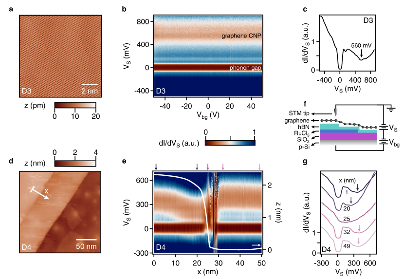
We use scanning tunneling microscopy and spectroscopy at K to study the spatial variation of the Dirac point across differentially-doped regions in two other devices, D3 and D4, both composed of overlapping flakes of graphene, hBN, and -RuCl3 on a SiO2/-Si substrate. Figure 3a shows an atomically resolved topographic map of a region in D3, consisting of graphene in direct contact with -RuCl3. The differential tunneling current, d/d, proportional to the local density of states (LDOS), is acquired as a function of the tip-sample bias, , and a back gate voltage applied to the substrate, , with results plotted in Fig. 3b where a dark blue (brown) color corresponds to high (low) LDOS. A strong dark brown band centered about mV appears along with several fainter features. We show the averaged spectra from V to V in Fig. 3c which shows a 120-mV-wide U-shaped suppression of d/d centered about mV, with a less pronounced minimum at mV. The former is a familiar phonon-assisted inelastic tunneling gap 34, while the latter corresponds to the graphene CNP 34, 35. We estimate the graphene carrier density using , with the phonon energy and the energy of the Dirac point in Fig. 3c, and find a large -type doping of , on the low side of prior observations of the graphene/-RuCl3 charge transfer19, 18, 23. The surprising lack of response to the back gate corroborates the screening effect noted above in transport for -RuCl3-doped graphene.
In Fig. 3d, we show a topographic map of a region in device D4 that shows terraces due to separation of graphene and -RuCl3 by an hBN spacer of varying thickness, shown schematically in Fig. 3f. In Fig. 3e, we show d/d spectra acquired over one such edge (along the arrow in Fig. 3d) as a function of both and position to map the change in charge transfer. The white curve shows the height profile (right axis). As above, the phonon gap appears at mV, but the graphene CNP feature disperses non-monotonically with , briefly decreasing as the step edge is approached and then sharply increasing to a final plateau once the step edge is crossed. Point spectroscopy taken at different values (shown in Fig. 3g) illustrates the non-monotonic variation of the CNP across the step edge. Far from the edge, the charge density is found to be () for the higher (lower) step, confirming that larger charge transfers are associated with thinner hBN spacer layers. The positive shift of the CNP takes place rapidly over . A recent work in which STM is used to map the charge density in a nanobubble in graphene on -RuCl3, at room temperature, finds an even sharper interface across a junction36. We note an instability in STS is observed at the step edge, where the tip-sample interaction may lead to a small delamination of the graphene with a decrease in the charge transfer 37.
To understand both the lateral and vertical spatial distribution of the charge transfer due to the modulation-doping of graphene by -RuCl3, we perform first principles calculations of a monolayer-thick -RuCl3 ribbon on graphene as shown in Fig. 4a and b. By using DFT calculations as implemented in VASP25, we first calculate the properties of the interface when no spacer layers are present in a large supercell in the ribbon-on-sheet geometry (see Fig. 4a), with supercell lattice parameters =34.16 Å, =9.84 Å and =20 Å (distance between periodic images along direction is 16.5 Å), and the graphene C-C bond-lengths fixed at 1.42 Å. Geometrical optimization of the internal atomic degrees of freedom leads to a mildly distorted Ru hexagon with shorter Ru-Ru bonds (=3.17 Å) arranged in a periodic-step-function like pattern along the direction , compared with the other Ru-Ru bonds of the ribbon (=3.48-3.52 Å).
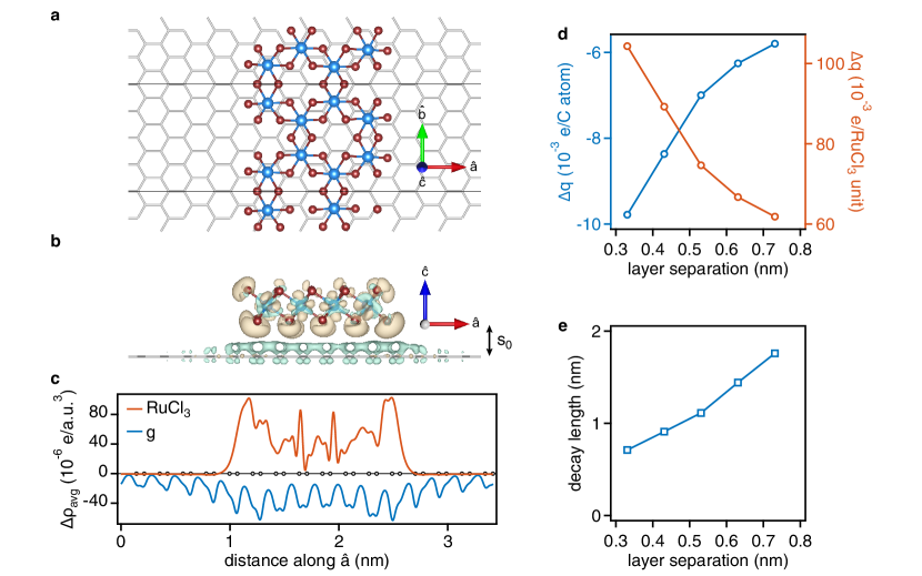
With the two materials in close proximity, a new charge density distribution develops which we illustrate by subtracting of the charge densities of intrinsic graphene and -RuCl3 from that of the graphene/-RuCl3 heterostructure, . We find that charge accumulates in the -RuCl3 ribbon with a concomitant depletion in the graphene, as shown in Fig. 4b where we plot the charge isosurface at /a.u.3, and in Fig. 4c by directly plotting the variations in the planar average of (over ) along the direction for the graphene and -RuCl3 layers. These results are in accord with findings for the graphene/-RuCl3 commensurate bilayer case 22. Figure 4c shows the excess electronic charge in -RuCl3 tends to lie largely on the Cl atoms facing the graphene. The majority of the charge depletion in graphene is concentrated at the C atom locations underneath the -RuCl3, reaches maxima near the boundaries of the -RuCl3 ribbon, and proceeds to decrease rapidly beyond the edge. Adding a second -RuCl3 layer does not qualitatively alter this result 25.
The equilibrium height of the -RuCl3 above the graphene, Å, is defined as the average distance between the C atoms in graphene and the graphene-facing Cl atoms in -RuCl3, shown in Fig. 4b. To mimic the presence of a dielectric spacer layer, we calculate how the charge transfer changes if the separation is increased up to an additional 4 Å (without further relaxing the geometry, but with the supercell lattice parameter also increased up to 24 Å). The results, in Fig. 4d, show a clear decrease of the charge exchange between the two layers, in qualitative agreement with the experimentally observed modulation doping effect. Performing the calculation with a dielectric present would alter the absolute magnitude of charge transfer but is expected to keep the relative changes similar to what we have found here 18.
Finally, we can estimate the characteristic length scale over which the charge transfer decays away outside the ribbon by fitting the decrease of the charge density peaks around the C atoms, visible in Fig. 4c, as a function of distance. We find the best fit to the data is made using an equation of the form , with measured along from the average position of the zigzag C atoms just outside the -RuCl3 ribbon. The decay length, , plotted in Fig. 4e is an average of the fits made on either side of the -RuCl3 ribbon, and is found to be roughly 2.5 times greater than the graphene/-RuCl3 separation 25.
We have demonstrated ultra-sharp junctions in modulation-doped graphene devices. This innovation relies upon several advantages conferred by using -RuCl3 to charge dope graphene.
First, we use a cleaved crystalline edge to define an atomically-sharp and straight interface along the several-micron-length of the - junction. Prior work has determined that roughness of this interface can be a significant hurdle to achieving ultra-sharp junctions38. This advantage is not unique to -RuCl3; however, even in cleaved graphite-gate-defined - devices with sub-nm lateral roughness along the interface, 40-nm-wide junctions still are observed17. Thus a sharp interface may be necessary but is apparently not sufficient to obtain ultra-sharp junctions.
Therefore we note additional advantages unique to the -RuCl3 approach. Our devices are composed of two monolayer charge distributions (only the layer of -RuCl3 closest to graphene is appreciably charged 18, 25). These form a nearly ideal parallel-plate capacitor geometry with arbitrarily small separation between the plates. Indeed, the charge distribution in the -RuCl3 shows accumulation near the edge of the ribbon, visible in Fig. 4c, just as expected for a classical charged sheet over a metallic plane. This suggests the extent of the potential variation in graphene beyond the edge of -RuCl3 (e.g. the junction width) is, apart from a possible role for nonlinear screening 30, essentially a matter of electrostatics and thus due to the usual fringing electric fields which have a lateral extent on the order of the plate separation. Given this, it should be possible to achieve a similar result by implementing a graphite gate just as close to the graphene; however, this presents numerous practical difficulties including dielectric breakdown, unwanted leakage currents to the conducting gate, and the onset of tunneling for dielectric thicknesses below 2 nm39. These are not limitations for -RuCl3-doped graphene, for which the charge transfer is fixed, requires no external bias, and crucially has no leakage current due to the insulating nature of -RuCl3.
Thus the narrowest junctions can be achieved by placing a flake of -RuCl3 with a cleaved edge as close as possible to the graphene. Junctions defined in this manner should be narrow enough to enable observation of electron-optical effects such as Veselago lensing and other useful devices based on electron refraction or reflection6.
Additional information on sample preparation and device fabrication, device mobilities and mean free paths, identification of -RuCl3 crystallographic edges, analysis of junction resistance data, scanning tunneling measurements, details of density functional theory calculations, and screening of back gate by -RuCl3.
We acknowledge enjoyable and informative discussions with K. Burch, D. Basov, Y. Wang, E. Gerber, and D. Rizzo. Support for device fabrication and measurement by the Institute of Materials Science and Engineering at Washington University in St. Louis is gratefully acknowledged. E.A.H., J.B., and J.B. received partial support from the National Science Foundation under DMR-1810305, and E.A.H. was additionally supported by NSF CAREER DMR-1945278. S.L. was supported by Office of Naval Research 6.1 Base Funding and the Jerome and Isabella Distinguished Scholar Fellowship. K.W. and T.T. acknowledge support from the Elemental Strategy Initiative conducted by the MEXT, Japan (Grant Number JPMXP0112101001) and JSPS KAKENHI (Grant Numbers 19H05790, 20H00354 and 21H05233). J.V.J. and Z.G. acknowledge support from the National Science Foundation under award DMR-1753367. J.V.J. acknowledges support from the Army Research Office under contract W911NF-17-1-0473. S.B. and R.V. thank the Deutsche Forschungsgemeinschaft (DFG, German Research Foundation)-TRR 288-422213477 (Project A05). M.C. and D.M. were supported by the National Science Foundation, Grant No. DMR-1808964.
References
- Katsnelson et al. 2006 Katsnelson, M. I.; Novoselov, K. S.; Geim, A. Chiral tunnelling and the Klein paradox in graphene. Nature Physics 2006, 2, 620–625
- Stander et al. 2009 Stander, N.; Huard, B.; Goldhaber-Gordon, D. Evidence for Klein Tunneling in Graphene p-n Junctions. Physical Review Letters 2009, 102, 026807
- Young and Kim 2009 Young, A. F.; Kim, P. Quantum interference and Klein tunnelling in graphene heterojunctions. Nature Physics 2009, 5, 222–226
- Allain and Fuchs 2011 Allain, P. E.; Fuchs, J. N. Klein tunneling in graphene: optics with massless electrons. The European Physical Journal B 2011, 83, 301–317
- Cheianov et al. 2007 Cheianov, V. V.; Fal’ko, V.; Altshuler, B. L. The focusing of electron flow and a Veselago lens in graphene p-n junctions. Science 2007, 315, 1252
- Chen et al. 2016 Chen, S.; Han, Z.; Elahi, M. M.; Habib, K. M. M.; Wang, L.; Wen, B.; Gao, Y.; Taniguchi, T.; Watanabe, K.; Hone, J.; Ghosh, A. W.; Dean, C. R. Electron optics with p-n junctions in ballistic graphene. Science 2016, 353, 1522–1525
- Mishchenko et al. 2010 Mishchenko, E. G.; Shytov, A. V.; Silvestrov, P. G. Guided Plasmons in Graphene p-n Junctions. Physical Review Letters 2010, 104, 156806
- Williams and Marcus 2011 Williams, J. R.; Marcus, C. M. Snake States along Graphene p-n Junctions. Physical Review Letters 2011, 107, 046602
- Park et al. 2008 Park, C.; Yang, L.; Son, Y.; Cohen, M.; Louie, S. Anisotropic behaviours of massless Dirac fermions in graphene under periodic potentials. Nature Physics 2008, 4, 213–217
- Li et al. 2021 Li, Y.; Dietrich, S.; Forsythe, C.; Taniguchi, T.; Watanabe, K.; Moon, P.; Dean, C. R. Anisotropic band flattening in graphene with one-dimensional superlattices. Nature Nanotechnology 2021, 16, 525–530
- Vakil and Engheta 2011 Vakil, A.; Engheta, N. Transformation Optics Using Graphene. Science 2011, 332, 1291–1294
- Park et al. 2008 Park, C.-H.; Son, Y.-W.; Yang, L.; Cohen, M. L.; Louie, S. G. Electron Beam Supercollimation in Graphene Superlattices. Nano Letters 2008, 8, 2920–2924
- Sajjad and Ghosh 2011 Sajjad, R. N.; Ghosh, A. W. High efficiency switching using graphene based electron “optics”. Applied Physics Letters 2011, 99, 123101
- Péterfalvi et al. 2012 Péterfalvi, C. G.; Oroszlány, L.; Lambert, C. J.; Cserti, J. Intraband electron focusing in bilayer graphene. New Journal of Physics 2012, 14, 063028
- Jang et al. 2013 Jang, M. S.; Kim, H.; Son, Y.-W.; Atwater, H. A.; Goddard, W. A. Graphene field effect transistor without an energy gap. Proceedings of the National Academy of Sciences 2013, 110, 8786–8789
- Lee et al. 2015 Lee, G.-H.; Park, G.-H.; Lee, H.-J. Observation of negative refraction of Dirac fermions in graphene. Nature Physics 2015, 11, 925–929
- Zhou et al. 2019 Zhou, X.; Kerelsky, A.; Elahi, M. M.; Wang, D.; Habib, K. M. M.; Sajjad, R. N.; Agnihotri, P.; Lee, J. U.; Ghosh, A. W.; Ross, F. M.; Pasupathy, A. N. Atomic-Scale Characterization of Graphene p–n Junctions for Electron-Optical Applications. ACS Nano 2019, 13, 2558
- Wang et al. 2020 Wang, Y. et al. Modulation Doping via a Two-Dimensional Atomic Crystalline Acceptor. Nano Letters 2020, 20, 8446
- Zhou et al. 2019 Zhou, B.; Balgley, J.; Lampen-Kelley, P.; Yan, J.-Q.; Mandrus, D. G.; Henriksen, E. A. Evidence for charge transfer and proximate magnetism in graphene–-RuCl3 heterostructures. Physical Review B 2019, 100, 165426
- Mashhadi et al. 2019 Mashhadi, S.; Kim, Y.; Kim, J.; Weber, D.; Taniguchi, T.; Watanabe, K.; Park, N.; Lotsch, B.; Smet, J. H.; Burghard, M.; Kern, K. Spin-Split Band Hybridization in Graphene Proximitized with -RuCl3 Nanosheets. Nano Letters 2019, 19, 4659–4665
- Gerber et al. 2020 Gerber, E.; Yao, Y.; Arias, T. A.; Kim, E.-A. Ab Initio Mismatched Interface Theory of Graphene on -RuCl3: Doping and Magnetism. Physical Review Letters 2020, 124, 106804
- Biswas et al. 2019 Biswas, S.; Li, Y.; Winter, S. M.; Knolle, J.; Valenti, R. Electronic Properties of -RuCl3 in Proximity to Graphene. Physical Review Letters 2019, 123, 237201
- Rizzo et al. 2020 Rizzo, D. J. et al. Charge-Transfer Plasmon Polaritons at Graphene/-RuCl3 Interfaces. Nano Letters 2020, 20, 8438–8445
- Dingle et al. 1978 Dingle, R.; Störmer, H. L.; Gossard, A. C.; Wiegmann, W. Electron mobilities in modulation‐doped semiconductor heterojunction superlattices. Applied Physics Letters 1978, 33, 665–667
- 25 See Supporting Information
- Wang et al. 2019 Wang, K.; Elahi, M. M.; Wang, L.; Habib, K. M. M.; Taniguchi, T.; Watanabe, K.; Hone, J.; Ghosh, A. W.; Lee, G.-H.; Kim, P. Graphene transistor based on tunable Dirac fermion optics. Proceedings of the National Academy of Sciences 2019, 116, 6575–6579
- Chandni et al. 2015 Chandni, U.; Henriksen, E. A.; Eisenstein, J. P. Transport in indium-decorated graphene. Physical Review B 2015, 91, 245402
- Cheianov and Fal’ko 2006 Cheianov, V.; Fal’ko, V. Selective transmission of Dirac electrons and ballistic magnetoresistance of n-p junctions in graphene. Physical Review B 2006, 74, 041403
- Low et al. 2009 Low, T.; Hong, S.; Appenzeller, J.; Datta, S.; Lundstrom, M. S. Conductance Asymmetry of Graphene p-n Junction. IEEE Transactions on Electron Devices 2009, 56, 1292–1299
- Zhang and Fogler 2008 Zhang, L.; Fogler, M. Nonlinear Screening and Ballistic Transport in a Graphene - Junction. Physical Review Letters 2008, 100, 116804
- Fogler et al. 2008 Fogler, M. M.; Novikov, D. S.; Glazman, L. I.; Shklovskii, B. I. Effect of disorder on a graphene p-n junction. Physical Review B 2008, 77, 075420
- Huard et al. 2007 Huard, B.; Sulpizio, J.; Stander, N.; Todd, K.; Yang, B.; Goldhaber-Gordon, D. Transport Measurements Across a Tunable Potential Barrier in Graphene. Physical Review Letters 2007, 98, 236803
- Sajjad and Ghosh 2013 Sajjad, R. N.; Ghosh, A. W. Manipulating Chiral Transmission by Gate Geometry: Switching in Graphene with Transmission Gaps. ACS Nano 2013, 7, 9808–9813
- Zhang et al. 2008 Zhang, Y.; Brar, V. W.; Wang, F.; Girit, c. O.; Yayon, Y.; Panlasigui, M.; Zettl, A.; Crommie, M. F. Giant phonon-induced conductance in scanning tunnelling spectroscopy of gate-tunable graphene. Nature Physics 2008, 4, 627–630
- Zhang et al. 2009 Zhang, Y.; Brar, V. W.; Girit, c. O.; Zettl, A.; Crommie, M. F. Origin of spatial charge inhomogeneity in graphene. Nature Physics 2009, 5, 722–726
- Rizzo et al. 2022 Rizzo, D. J. et al. Nanometer-Scale Lateral p–n Junctions in Graphene/-RuCl3 Heterostructures. Nano Letters 2022, 22, 1946–1953
- Klimov et al. 2012 Klimov, N. N.; Jung, S.; Zhu, S.; Li, T.; Wright, C. A.; Solares, S. D.; Newell, D. B.; Zhitenev, N. B.; Stroscio, J. A. Electromechanical Properties of Graphene Drumheads. Science 2012, 336, 1557–1561
- Elahi et al. 2019 Elahi, M. M.; Masum Habib, K. M.; Wang, K.; Lee, G.-H.; Kim, P.; Ghosh, A. W. Impact of geometry and non-idealities on electron “optics” based graphene p-n junction devices. Applied Physics Letters 2019, 114, 013507
- Britnell et al. 2012 Britnell, L.; Gorbachev, R. V.; Jalil, R.; Belle, B. D.; Schedin, F.; Katsnelson, M. I.; Eaves, L.; Morozov, S. V.; Mayorov, A. S.; Peres, N. M. R.; Castro Neto, A. H.; Leist, J.; Geim, A. K.; Ponomarenko, L. A.; Novoselov, K. S. Electron Tunneling through Ultrathin Boron Nitride Crystalline Barriers. Nano Letters 2012, 12, 1707–1710
See pages - of ultrasharp_SI_resub.pdf