Variable and orbital-dependent spin-orbit field orientations in a InSb double quantum dot characterized via dispersive gate sensing
Abstract
Utilizing dispersive gate sensing (DGS), we investigate the spin-orbit field () orientation in a many-electron double quantum dot (DQD) defined in an InSb nanowire. While characterizing the inter-dot tunnel couplings, the measured dispersive signal depends on the electron charge occupancy, as well as on the amplitude and orientation of the external magnetic field. The dispersive signal is mostly insensitive to the external field orientation when a DQD is occupied by a total odd number of electrons. For a DQD occupied by a total even number of electrons, the dispersive signal is reduced when the finite external magnetic field aligns with the effective orientation. This fact enables the identification of orientations for different DQD electron occupancies. The orientation varies drastically between charge transitions, and is generally neither perpendicular to the nanowire nor in the chip plane. Moreover, is similar for pairs of transitions involving the same valence orbital, and varies between such pairs. Our work demonstrates the practicality of DGS in characterizing spin-orbit interactions in quantum dot systems, without requiring any current flow through the device.
A spinful carrier moving in an electromagnetic field may experience a coupling between its spin and momentum degree of freedom, namely spin-orbit interaction (SOI). The SOI allows spin manipulation with electric fields in semiconductor platforms, such that it enables electric dipole spin resonance [1, 2, 3, 4], spin-cavity couplings [5, 6, 7, 8], while it also enhances effects detrimental to spin-based quantum information processing: relaxation and decoherence [9, 10]. For many cases, SOI can be described as an effective spin-orbit field () acting on the carriers. Notably, associated with the Rashba SOI is perpendicular to both the electric field and the carrier momentum , following [11, 12]. In ideal nanowire systems, carriers are confined in a one-dimensional path, which forces their momentum to be along the nanowire. With the application of bottom electrostatic gates, the assumed electric field is perpendicular to the substrate surface. Accordingly, the orientation is expected and has been experimentally proved to be not only in-plane of the chip, but also nearly perpendicular to a bottom-gated nanowire [12, 13]. Despite the electrostatic confinement, this conclusion is further found to hold for electron tunneling in few-electron double quantum dots (DQD), even when the center-to-center distance between the dots is small with respect to typical spin orbit lengths [14, 15, 16]. Knowing the orientation in such nanowires is particularly important for semiconductor-superconductor hybrid systems that aim to realize Majorana zero modes, as setting the external magnetic field perpendicular to is a precondition to open a topological gap [17].
The conventional way to characterize SOI is associated with tunneling between quantum dots, which employs bias voltages across a DQD segment and measurements of spin blockade leakage current [18, 19, 14, 20]. However, scalable qubit devices [21, 22] may favor characterization methods that do not require transport measurements. Here, we explore dispersive gate sensing (DGS) [23, 8, 24, 25, 26, 27, 28] to characterize SOI, especially the orientation. Our protocol does not employ transport measurements, is compatible with fast data acquisition in rastering schemes [29, 25], and is promising for the integration of qubit characterization and readout capabilities [30, 31].
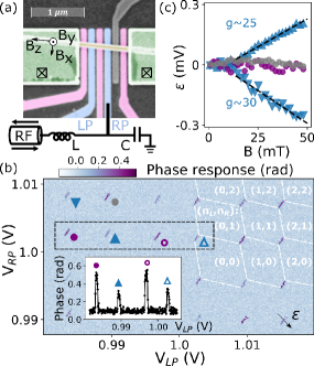
The device under study is depicted in Fig. 1(a). An InSb nanowire is placed on top of prefabricated bottom finger gates. The barrier gates confine the electrons and control the tunnel coupling within the DQD, while the plunger gates LP (RP) tune the chemical potential of the left (right) dot. The nanowire is grown along [111] direction, such that the Rashba SOI is expected to be dominant [14, 13, 32] To implement DGS, the RP gate is coupled to an off-chip superconducting spiral-inductor resonator, with resonance frequency 318.4 MHz and nominal inductance 730 nH [33]. At interdot charge transitions (ICTs), where the chemical potential for an electron residing in the left and the right dot are equal, the hybridization of electron wave functions between the two dots leads to an additional quantum capacitance loading the resonator, which is observable as a shift of [34, 35, 23, 25]. While fixing the probing frequency and detecting the reflected signal from the resonator, is translated into a change of reflection coefficient, thus to the amplitude and phase response. In this letter, we fit the measured reflection coefficient with an analytical resonator model to extract and (see Suppl. A). All measurements were performed in a dilution refrigerator at a base temperature 30 mK.
In Fig. 1(b), the charge stability diagram of the DQD is mapped by measuring the reflected phase response versus gate voltages and . It reveals a grid of ICTs with the lead-to-dot transitions hardly visible (marked by white lines), since the outer barrier gates are nearly pinched off. Along and axes, both the spacings between the ICTs and the measured phase shifts at the ICTs tend to alternate between smaller and larger values (inset of Fig. 1(b)). As loading every other additional electron requires compensating for the level spacing on top of the charging energy, the smaller spacings along () are associated with having an odd number of electrons in the left (right) dot [36]. Furthermore, an ICT corresponding to a total odd number of electrons in the DQD exhibit a larger phase shift, since the spin degeneracy of having total even charges leads to a reduction of the maximum of [4, 37, 26].
The identification of the total charge parity in the DQD is additionally verified by applying an external magnetic field (Fig. 1(c)) [38]. For four neighboring ICTs, their positions along the detuning axis are measured as a function of , with detuning . We observe shifts only for the ICTs with a total even occupancy, consistent with Zeeman effect. Fits to the data for even-occupied ICTs in a region exhibiting a linear shift in magnetic field [4] yield the effective g-factors of approximately 25 and 30. Based on these observations, the parity of the electron numbers in the DQD is indicated with labels , with indicating the excess number of electrons with respect to an even number of electrons on the left (right) dot (also indicated in Fig. 1(b)). The number of electrons in each dot is estimated to be in the range of 70 to 150 electrons, considering the plunger gate voltages, pinch off voltages, and the spacing between ICTs.
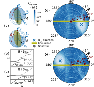
Having identified the total charge parity of the ICTs, we characterize the field orientation for an even-occupied ICT. We apply an external magnetic field with fixed amplitude mT. which denotes the maximum values of at the ICT (see Suppl. A) is extracted as a function of the field orientation in spherical coordinates and (Fig. 2(a)). Fig. 2 (d) and (e) display the obtained data in range , and , respectively. There are two regions at which is strongly suppressed. They lie at opposite directions in the spherical coordinates, neither perpendicular to the nanowire, nor in plane of the substrate. We interpret the centers of the suppression regions as corresponding to the directions parallel and anti-parallel to . Energy diagrams of the DQD are presented in Fig. 2(b,c). Due to different total spin, the lowest singlet state and triplet state only couple if electron spin flips during tunneling are allowed. This coupling arises only when is not aligned with (Fig. 2(b)), resulting in finite curvature of the ground state energy at the ICT, and thus finite . When , the two states do not couple (Fig. 2(c)), therefore is suppressed because of the flat energy dispersion of state [4, 39, 40].
The observation that is neither perpendicular to the nanowire nor in-plane of the chip can be attributed to several reasons. First, the complicated gate structure is likely to create a nonuniform potential, making the local electric fields deviate significantly from the out-of-plane direction. Second, staying in many-electron regime bring more complexity, as the overlap between the wave functions of the two dots may not spatially coincide with the direction of the nanowire. Consequently, the momentum associated with electron tunneling is not necessarily along the nanowire. Third, although not dominant, a finite contribution of Dresselhaus SOI may also exist, so that spin modulations in the cross-sectional plane contribute to the offset angle with respect to the chip plane [41].
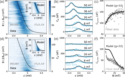
Next, we study the evolution of at the same ICT, as a function of and . While increasing the amplitude of , we find a nearly linear shift of the maximum along detuning axis (Fig. 3(a,b)). This is accompanied by a gradual increase of value (Fig. 3(c)), starting at about aF when is zero, and saturating near aF for above 25 mT. In contrast, is suppressed (Fig. 3(d-f)) for , since no longer introduces singlet-triplet coupling in this orientation. Along , the suppression occurs in two distinct steps (see Fig. 3(f)). Initially, drops rapidly from 100 aF for low , and starts saturating near the value of 50 aF with above 10 mT. Then, starts dropping even further at about 25 mT. In the limited measurement range, appears to be trending towards zero.
To understand the capacitative response of the ICT in magnetic field, we employ a two-site Hubbard model (Suppl. B) [42]. The SOI in our model is phenomenologically described as an effective field which can point in an arbitrary direction in space, namely both Rashba and Dresselhaus SOI are taken into consideration. The model includes the spin precessing tunneling matrix element as part of total tunneling strength . The term depends on the SOI strength and modulates spin-flip together with an angle between and . The individual cuts at and mT for are used to estimate eV and eV, by fitting the analytical expressions of in Suppl. B. For simplicity, we assume isotropic g-factors being equal in both dots, with the value taken from linear shifts of charge transitions as in Fig. 3(a). The effective lever arm of the gate attached to the resonator is , according to the ratio between the height and width of a Coulomb diamond, and an estimated crosstalk between the gates of . The electron temperature in the model is set to 30 mK, based on a Coulomb blockade thermometry measurement performed before this experiment. The simulated results are illustrated in the insets of Fig. 3(a,d), and in black in Fig. 3(b,c,e,f). For , we find an excellent agreement with the data in a full range of magnetic fields, with no free parameters. In contrast, for , the simulated shift of the ICT along detuning axis is greater than observed when is below 25 mT. Furthermore, the model does not qualitatively capture the two-stage suppression of when increases (Fig. 3(f)).
We identify two elements in our model potentially responsible for the discrepancy. First, we consider possible g-factor non-uniformity and anisotropy [14, 43, 44]. In particular, a smaller g-factor for can reduce the shift in detuning of the ICT in Fig. 3(d), and eventually increase at which the predicted suppression of occurs. Second, when , spin relaxation rates mediated by hyperfine and SOI are hindered [45, 46]. As a consequence, Pauli spin blockade traps the system in one of the excited states which do not contribute to . We hypothesize that unaccounted Pauli spin blockade is responsible for the suppression of the in range of 0-25 mT. Meanwhile, the suppression above 25 mT is consistent with our model, except it occurs at higher field due to an overestimated g-factor. This can be identified from comparing the peaks of model and data in Fig. 3(e).
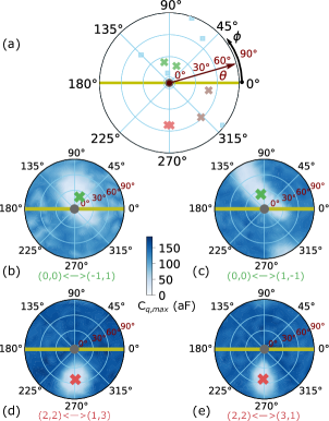
After analyzing an individual ICT, we look into the orientation of clusters of ICTs. We rotate while measuring for 16 neighboring ICTs (Suppl. C), where for odd-occupied ICTs, the extracted is independent of the orientation. On the contrary, the majority of even-occupied ICTs show a fairly well defined direction in which is suppressed, indicating the orientation of . A few of the ICTs reveal a suppression in a peculiar pattern with no clear preferred direction, which will be discussed later.
Fig. 4(a) summarizes all of the extracted orientations, including some cases where we tune the barrier and plunger gates by a large amount. The crosses with the same color indicate pairs of ICTs of the same valence orbital. The corresponding maps of extracted for two such ICT pairs are presented in Fig. 4(b-e). Blue squares in (a) indicate the ICTs for which the other ICT from a pair is not measured. Because of the inversion symmetry shown in Fig. 2(d-e), only the measurements for are performed.
The markers in Fig. 4(a) show no preferred direction among the complete set of measured orientations. Notably, for a pair of ICTs corresponding to the same valence orbital, their orientations are much closer to each other than to other random pairs. This thereby support the hypothesis that the random orientation of arises from the complex shape of the electronic orbitals and the hard-to-predict local . Imperfect alignment of the orientations within a pair of ICTs might be a consequence of a slight distortion of the confining potential, while the gates are tuning the dot occupancies. The irregular shape of the suppression regions for some of the ICTs (e.g. Fig. 4(c)) demonstrates that the description of SOI in terms of effective and isotropic g-factors is incomplete. In Ref. [47], Scheübl et al. discuss a topological nature of Weyl points between the lowest singlet and triplet states, which is equivalently manifested by the suppression of in our experiment. They show that the number of such Weyl points is not restricted to be 2 (like in Fig. 2(d-e)), but may be 6 or even larger for rare cases. The presence of more than 2 Weyl points might explain the highly irregular regions of suppression for some ICTs.
In summary, we study orientation using DGS in an InSb nanowire-based DQD. At zero magnetic field, DGS can be employed as a charge parity meter, and ICTs with even total parity are identified for further characterization. When a finite external field is rotated, the directions in which is suppressed reveal the orientation of even-occupied ICTs. We model the dispersive signal at an even-occupied ICT, and find good agreement with the data for . However, for , our model lacks a description of the suppressed spin relaxation rates due to Pauli blockade. Finally, we find that for the ICT pairs with the same valence orbital have similar orientations, while the orientation varies enormously between different orbitals. Our work indicates that considerations about orientation based purely on device design may often not apply to quantum dot systems. Resolving whether the randomness of orientation persists in quantum devices, either based on nanowires or two-dimensional electron gases, is essential to assess the viability of different materials for quantum computing with spins and Majorana zero modes. Moreover, DGS is shown to be an effective tool in characterizing the orientation, especially when transport measurements are not applicable. This result also opens new prospects for systems applying DGS that feature integrated capabilities for qubit characterization and readout, while avoiding increasing the complexity in the chip design [30, 31, 48].
I Acknowledgement
We appreciate J. Koski for suggestions regarding to the experiment and the manuscript. We thank K. Li for assisting nanowire deposition, F. Borsoi, N. van Loo and J. Wang for useful advice on fabrication, A. Palyi and Z. Scherübl for fruitful discussions on the measurement results, also M. Hornibrook and D.J. Reilly for providing the frequency multiplexing chips, O.W.B. Benningshof, R.N. Schouten, and J.D. Mensingh for valuable technical assistance. This work has been supported by the Netherlands Organization for Scientific Research (NWO) and Microsoft Quantum Lab Delft. FKM acknowledges support from NWO under Veni grant (VI.Veni.202.034).
References
- Rashba and Efros [2003] E. Rashba and A. L. Efros, Physical review letters 91, 126405 (2003).
- Žutić et al. [2004] I. Žutić, J. Fabian, and S. D. Sarma, Reviews of modern physics 76, 323 (2004).
- Golovach et al. [2006] V. N. Golovach, M. Borhani, and D. Loss, Physical Review B 74, 165319 (2006).
- Hanson et al. [2007] R. Hanson, L. P. Kouwenhoven, J. R. Petta, S. Tarucha, and L. M. Vandersypen, Reviews of modern physics 79, 1217 (2007).
- Nadj-Perge et al. [2010a] S. Nadj-Perge, S. Frolov, E. Bakkers, and L. P. Kouwenhoven, Nature 468, 1084 (2010a).
- Petersson et al. [2012] K. D. Petersson, L. W. McFaul, M. D. Schroer, M. Jung, J. M. Taylor, A. A. Houck, and J. R. Petta, Nature 490, 380 (2012).
- Tarucha et al. [2016] S. Tarucha, M. Yamamoto, A. Oiwa, B.-S. Choi, and Y. Tokura, in Principles and Methods of Quantum Information Technologies (Springer, 2016) pp. 541–567.
- Crippa et al. [2019] A. Crippa, R. Ezzouch, A. Aprá, A. Amisse, R. Laviéville, L. Hutin, B. Bertrand, M. Vinet, M. Urdampilleta, T. Meunier, et al., Nature communications 10, 1 (2019).
- Kloeffel and Loss [2013] C. Kloeffel and D. Loss, Annu. Rev. Condens. Matter Phys. 4, 51 (2013).
- Chatterjee et al. [2021] A. Chatterjee, P. Stevenson, S. De Franceschi, A. Morello, N. P. de Leon, and F. Kuemmeth, Nature Reviews Physics 3, 157 (2021).
- Winkler et al. [2003] R. Winkler, S. Papadakis, E. De Poortere, and M. Shayegan, Spin-Orbit Coupling in Two-Dimensional Electron and Hole Systems, Vol. 41 (Springer, 2003).
- Ihn [2009] T. Ihn, Semiconductor Nanostructures: Quantum states and electronic transport (OUP Oxford, 2009).
- Kammhuber et al. [2017] J. Kammhuber, M. C. Cassidy, F. Pei, M. P. Nowak, A. Vuik, O. Gul, D. Car, S. Plissard, E. Bakkers, M. Wimmer, et al., Nature communications 8, 1 (2017).
- Nadj-Perge et al. [2012] S. Nadj-Perge, V. Pribiag, J. Van den Berg, K. Zuo, S. Plissard, E. Bakkers, S. Frolov, and L. Kouwenhoven, Physical review letters 108, 166801 (2012).
- Wang et al. [2018] J.-Y. Wang, G.-Y. Huang, S. Huang, J. Xue, D. Pan, J. Zhao, and H. Xu, Nano letters 18, 4741 (2018).
- Dorsch et al. [2019] S. Dorsch, B. Dalelkhan, S. Fahlvik, and A. Burke, Nanotechnology 30, 144002 (2019).
- Lutchyn et al. [2018] R. M. Lutchyn, E. P. Bakkers, L. P. Kouwenhoven, P. Krogstrup, C. M. Marcus, and Y. Oreg, Nature Reviews Materials 3, 52 (2018).
- Pfund et al. [2007] A. Pfund, I. Shorubalko, K. Ensslin, and R. Leturcq, Physical Review B 76, 161308 (2007).
- Nadj-Perge et al. [2010b] S. Nadj-Perge, S. Frolov, J. Van Tilburg, J. Danon, Y. V. Nazarov, R. Algra, E. Bakkers, and L. Kouwenhoven, Physical Review B 81, 201305 (2010b).
- Bogan et al. [2021] A. Bogan, S. Studenikin, M. Korkusinski, L. Gaudreau, J. Phoenix, P. Zawadzki, A. Sachrajda, L. Tracy, J. Reno, and T. Hargett, Physical Review B 103, 235310 (2021).
- Zajac et al. [2016] D. Zajac, T. Hazard, X. Mi, E. Nielsen, and J. R. Petta, Physical Review Applied 6, 054013 (2016).
- Karzig et al. [2017] T. Karzig, C. Knapp, R. M. Lutchyn, P. Bonderson, M. B. Hastings, C. Nayak, J. Alicea, K. Flensberg, S. Plugge, Y. Oreg, et al., Physical Review B 95, 235305 (2017).
- Colless et al. [2013] J. Colless, A. Mahoney, J. Hornibrook, A. Doherty, H. Lu, A. Gossard, and D. Reilly, Physical review letters 110, 046805 (2013).
- Zheng et al. [2019] G. Zheng, N. Samkharadze, M. L. Noordam, N. Kalhor, D. Brousse, A. Sammak, G. Scappucci, and L. M. Vandersypen, Nature nanotechnology 14, 742 (2019).
- De Jong et al. [2019] D. De Jong, J. Van Veen, L. Binci, A. Singh, P. Krogstrup, L. P. Kouwenhoven, W. Pfaff, and J. D. Watson, Physical Review Applied 11, 044061 (2019).
- Van Veen et al. [2019] J. Van Veen, D. De Jong, L. Han, C. Prosko, P. Krogstrup, J. D. Watson, L. P. Kouwenhoven, and W. Pfaff, Physical Review B 100, 174508 (2019).
- Sabonis et al. [2019] D. Sabonis, E. C. O’Farrell, D. Razmadze, D. M. van Zanten, J. Suter, P. Krogstrup, and C. M. Marcus, Applied Physics Letters 115, 102601 (2019).
- De Jong et al. [2020] D. De Jong, D. Waardenburg, N. Blaznik, L. Han, F. Malinowski, C. Prosko, J. Van Veen, P. Krogstrup, L. Kouwenhoven, and W. Pfaff, Bulletin of the American Physical Society 65 (2020).
- Stehlik et al. [2015] J. Stehlik, Y.-Y. Liu, C. Quintana, C. Eichler, T. Hartke, and J. R. Petta, Physical Review Applied 4, 014018 (2015).
- Plugge et al. [2017] S. Plugge, A. Rasmussen, R. Egger, and K. Flensberg, New Journal of Physics 19, 012001 (2017).
- Smith et al. [2020] T. B. Smith, M. C. Cassidy, D. J. Reilly, S. D. Bartlett, and A. L. Grimsmo, PRX Quantum 1, 020313 (2020).
- Badawy et al. [2019] G. Badawy, S. Gazibegovic, F. Borsoi, S. Heedt, C.-A. Wang, S. Koelling, M. A. Verheijen, L. P. Kouwenhoven, and E. P. Bakkers, Nano letters 19, 3575 (2019).
- Hornibrook et al. [2014] J. Hornibrook, J. Colless, A. Mahoney, X. Croot, S. Blanvillain, H. Lu, A. Gossard, and D. Reilly, Applied Physics Letters 104, 103108 (2014).
- Duty et al. [2005] T. Duty, G. Johansson, K. Bladh, D. Gunnarsson, C. Wilson, and P. Delsing, Physical review letters 95, 206807 (2005).
- Petersson et al. [2010] K. Petersson, C. Smith, D. Anderson, P. Atkinson, G. Jones, and D. Ritchie, Nano letters 10, 2789 (2010).
- Van der Wiel et al. [2002] W. G. Van der Wiel, S. De Franceschi, J. M. Elzerman, T. Fujisawa, S. Tarucha, and L. P. Kouwenhoven, Reviews of Modern Physics 75, 1 (2002).
- Cottet et al. [2011] A. Cottet, C. Mora, and T. Kontos, Physical Review B 83, 121311 (2011).
- Schroer et al. [2012] M. Schroer, M. Jung, K. Petersson, and J. R. Petta, Physical review letters 109, 166804 (2012).
- Mizuta et al. [2017] R. Mizuta, R. Otxoa, A. Betz, and M. F. Gonzalez-Zalba, Physical Review B 95, 045414 (2017).
- Esterli et al. [2019] M. Esterli, R. Otxoa, and M. Gonzalez-Zalba, Applied Physics Letters 114, 253505 (2019).
- Bringer et al. [2019] A. Bringer, S. Heedt, and T. Schäpers, Physical Review B 99, 085437 (2019).
- Ziesche et al. [1997] P. Ziesche, O. Gunnarsson, W. John, and H. Beck, Physical Review B 55, 10270 (1997).
- Qu et al. [2016] F. Qu, J. van Veen, F. K. de Vries, A. J. Beukman, M. Wimmer, W. Yi, A. A. Kiselev, B.-M. Nguyen, M. Sokolich, M. J. Manfra, et al., Nano letters 16, 7509 (2016).
- Mu et al. [2020] J. Mu, S. Huang, J.-Y. Wang, G.-Y. Huang, X. Wang, and H. Xu, Nanotechnology 32, 020002 (2020).
- Fujita et al. [2016] T. Fujita, P. Stano, G. Allison, K. Morimoto, Y. Sato, M. Larsson, J.-H. Park, A. Ludwig, A. Wieck, A. Oiwa, et al., Physical Review Letters 117, 206802 (2016).
- Lundberg et al. [2021] T. Lundberg, D. J. Ibberson, J. Li, L. Hutin, J. C. Abadillo-Uriel, M. Filippone, B. Bertrand, A. Nunnenkamp, C.-M. Lee, N. Stelmashenko, et al., arXiv preprint arXiv:2110.09842 (2021).
- Scherübl et al. [2019] Z. Scherübl, A. Pályi, G. Frank, I. E. Lukács, G. Fülöp, B. Fülöp, J. Nygård, K. Watanabe, T. Taniguchi, G. Zaránd, et al., Communications Physics 2, 1 (2019).
- Maman et al. [2020] V. D. Maman, M. Gonzalez-Zalba, and A. Pályi, Physical Review Applied 14, 064024 (2020).