Microwave-frequency scanning gate microscopy of a Si/SiGe double quantum dot
Abstract
Conventional quantum transport methods can provide quantitative information on spin, orbital, and valley states in quantum dots, but often lack spatial resolution. Scanning tunneling microscopy, on the other hand, provides exquisite spatial resolution of the local electronic density of states, but often at the expense of speed. Working to combine the spatial resolution and energy sensitivity of scanning probe microscopy with the speed of microwave measurements, we couple a metallic probe tip to a Si/SiGe double quantum dot that is integrated with a local charge detector. We first demonstrate that a dc-biased tip can be used to change the charge occupancy of the double dot. We then apply microwave excitation through the scanning tip to drive photon-assisted tunneling transitions in the double dot. We infer the double dot energy level diagram from the frequency and detuning dependence of the photon-assisted tunneling resonance condition. These measurements allow us to resolve 65 eV excited states, an energy scale consistent with typical valley splittings in Si/SiGe. Future extensions of this approach may allow spatial mapping of the valley splitting in Si devices, which is of fundamental importance for spin-based quantum processors.
keywords:
American Chemical Society, LaTeXPrinceton Physics] Department of Physics, Princeton University, Princeton, NJ 08544, USA Princeton Physics] Department of Physics, Princeton University, Princeton, NJ 08544, USA Princeton Physics] Department of Physics, Princeton University, Princeton, NJ 08544, USA IAC] Princeton Institute for the Science and Technology of Materials, Princeton University, Princeton, New Jersey 08544, USA UCLA Math] Department of Mathematics, University of California, Los Angeles, CA 90095, USA UCLA Math] Center for Quantum Science and Engineering, University of California, Los Angeles, CA 90095, USA UW] Department of Physics, University of Washington, 98195 Seattle, Washington, USA UW_Mat] Department of Materials Science and Engineering, University of Washington, 98195 Seattle, Washington, USA Princeton Physics] Department of Physics, Princeton University, Princeton, NJ 08544, USA \abbreviationsQD,DQD,AFM,SGM
1 Introduction
Quantum device performance is generally characterized in terms of a few metrics, such as the qubit relaxation time, coherence time, and gate fidelity 1. In many systems the relationship between microscopic material parameters and coherence times is poorly understood. For example, the relaxation time of superconducting qubits is limited to 100’s of s 2. Charge noise is ubiquitous in semiconductor devices and limits the fidelity of both charge 3 and spin qubits 4. To link microscopic materials properties and qubit performance it is desirable to develop measurement approaches that combine high spatial resolution, control of realistic quantum devices, and operation at frequencies comparable to qubit transition frequencies (typically 5 – 20 GHz range).
Silicon spin qubits are among the leading contenders for building fault-tolerant quantum computers 5, 6 due to their small 100 footprint 7, 8 and the ability to chemically and isotopically purify the silicon host material. While long coherence times 9 and high fidelity gates 10, 11, 12, 13 have been achieved, there are concerns about how the valley degree of freedom may impact performance as the number of silicon spin qubits scales up 14, 15. The strain of the Si quantum well (QW) induced by the Si and SiGe lattice mismatch partially lifts the six-fold valley degeneracy present in bulk Si 16. However, failure to lift the degeneracy of the low lying -valleys can lead to an additional uncontrolled degree of freedom 17, 18, 19 and fast qubit relaxation 20. An abrupt Si/SiGe interface can lift the two-fold valley degeneracy, but in reality the interface is never perfectly sharp 21, 22, 23, 24. Combined with atomic-scale disorder, these effects lead to a large spread in reported valley splittings 25–300 eV 25, 19, 20, 26, 27, 28, 18. Progress in better understanding the limits of valley splitting in Si/SiGe has been impeded by the lack of measurement techniques that offer spatial resolution. To accelerate improvements in heterostructure growth, it is crucial to develop a scanning probe technique capable of measuring valley splitting with spatial resolution 29.
Scanning gate microscopy (SGM) provides spatial resolution, but it has not been applied to realistic quantum devices. In previous experiments, SGM was performed exclusively in quantum dots (QDs) defined by local anodic oxidation 30, 31 in doped GaAs or by using one layer of metallic gates 32. Additionally, multiple QDs accidentally formed in carbon nanotubes 33 or semiconductor nanowires 34 were studied. All of these structures have an essentially open surface with at most a few thin metallic gates to deplete electrons 35.
In this Letter we perform SGM on a device consisting of a lithographically defined double quantum dot (DQD) and an integrated QD charge sensor 36. The DQD is one of the most common building blocks used to define Si/SiGe charge and spin qubits 37. To allow for the integration of the DQD in a SGM experiment, we purposely omit a gate electrode, allowing the electric potential of the SGM tip to couple to electrons in the Si QW. Using the biased tip as a movable plunger gate we demonstrate manipulation and imaging of single electrons inside the device. In the few-electron regime, where the current through the device is pinched off, we show how the charge sensor signal can be used to count electrons. By applying a microwave tone through the tip, we are able to perform excited state spectroscopy by means of photon-assisted tunneling (PAT). Our work demonstrates microscope-based characterization and control of a semiconductor quantum device and may be further extended to investigations of spin and valley coherence with spatial resolution.
2 Results and discussion
Our device is fabricated on a Si/SiGe heterostructure (see Fig. 1a for a schematic of the experimental setup). The heterostructure consists of a thick Si QW that is buried by a thick layer of Si0.7Ge0.3 and capped by of Si. To control the electron density in the plane of the QW, we utilize a gate stack consisting of three overlapping layers of Al electrodes 8, with progressively increasing thicknesses of 25, 45, and . The gates define a DQD and an adjacent charge sensor QD as shown in Figs. 1b, c. The charge sensing QD 8 is formed by means of two barrier gates (B1, B2) and a plunger gate (P). Gates S1, P1, P2, and D1 are patterned in the upper half of the device. Here we purposely omit the middle gate electrode, since its functionality is to be replaced by the SGM tip. The middle slit-gate (MS) separates the upper and lower parts of the sample, such that the DQD (sensor) current () can be independently measured.
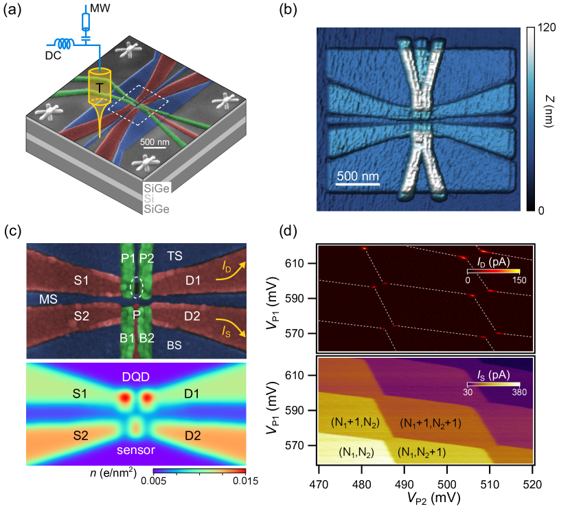
A metallic SGM tip may be used to perturb the electronic confinement potential in the Si QW. As sketched in Fig. 1a, a bias-T allows both a dc bias and microwave excitation to be applied to the tip. A typical low-temperature AFM topography image of a test structure similar to the device is shown in Fig. 1b. Here, all three layers of overlapping Al gates are visible and can be compared to the high resolution scanning electron microscope (SEM) image in Fig. 1c. All measurements were performed in cryogen-free Bluefors XLD dilution refrigerator at base electron temperature of 150 . Details of the active and passive vibration damping stages utilized in the dilution refrigerator are detailed elsewhere 38. We characterized three similar devices and obtained reproducible results. Data from one device are shown here.
We first discuss dc operation of the device with the SGM tip pulled far from the sample. We are able to tune the device shown in Fig. 1c to a regime where the gates P1 and P2 form a DQD. The lower panel of Fig. 1c shows the simulated charge density in the Si QW, with regions of high charge density near the ends of the S1 and D1 accumulation gates. The presence of the DQD is evident from the charge stability diagrams shown in Fig. 1d. The upper plot shows the current as a function of the gate voltages and with a small source-drain bias applied across the device (). As expected for weak interdot tunnel coupling 39, is nonzero only in the vicinity of a triple point, where electrons or holes can resonantly tunnel through the DQD. The dashed lines are guides to the eye and separate different DQD charge configurations. Charge states are denoted (, ), where () is the number of electrons in the left (right) dot. The lower panel of Fig. 1d shows the current over the same range of gate voltages. As expected, changes stepwise each time an electron is added to the DQD (thereby changing the total charge occupancy = +) 40. In contrast, the sensor is insensitive to interdot charge transitions (where + is constant) due to the fact that the sensor is symmetrically placed across from the DQD 41.
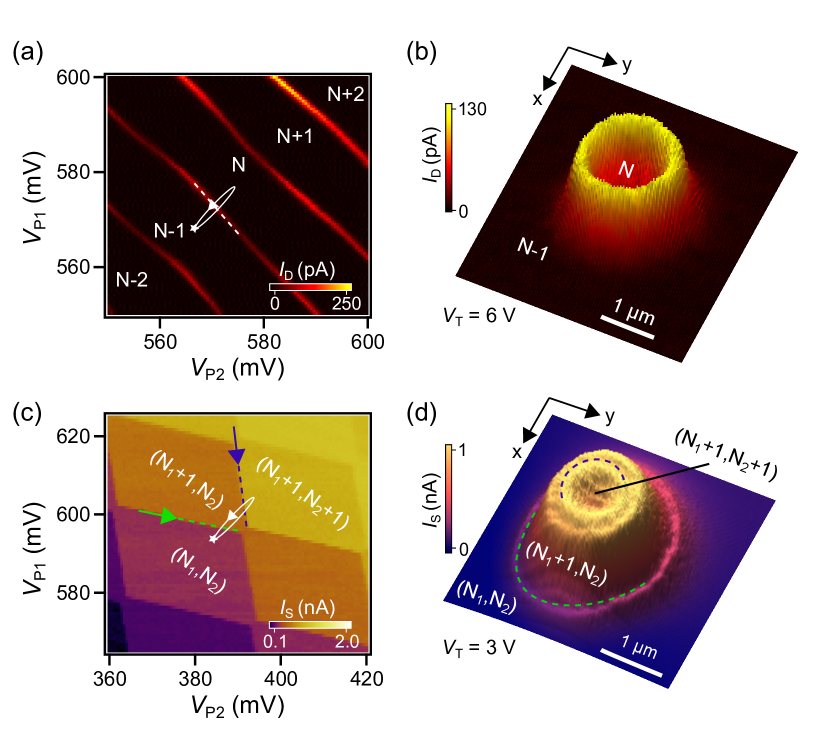
We now investigate the impact of the metallic SGM tip on the transport properties of the device. Large-scale scans over gate voltage space (,) show a crossover from single QD to DQD behavior 42 (see SM Fig. 1). The dot current acquired in the single QD regime is plotted in Fig. 2a. Here, due to cross-capacitance effects, the device acts as a single elongated QD. To acquire SGM data, we begin with the tip far from the device and set the gate voltages in the electron charge state (white star in Fig. 2a). The gate voltages are then held constant during SGM measurements. With the biased tip () parked 120 nm above the Al gates, we measure as a function of the coordinates of the tip, as shown in Fig. 2b.
The electrostatic confinement potential is dependent on the (,,) coordinates of the tip. As a result the charge stability diagram shifts to lower gate voltages (see SM Fig. 2) as we bring the positively biased tip closer to the QD. The circular feature in Fig. 2b marks the moment when the Coulomb peak separating the and charge states in Fig. 2a crosses the initial position in gate voltage space (marked as a white star in Fig. 2a). Equivalently, we can imagine the stability diagram unchanged and the tip instead traversing a certain trajectory in gate voltage space as shown by the white line in Fig. 2a. The almost perfectly circular feature in the SGM image defines the line of a constant tip-device interaction potential around the dot and separates the and charge states in the -plane 30, 32. Sweeping or moving the tip in -coordinate changes the electron occupancy of the dot. These effects are well-known 35 and we discuss them in the Supplementary Material 42 .
Operation in the few electron regime is required for the precise control of charge and spin qubits 43. Now we perform the same set of measurements in the few electron DQD regime (Fig. 2c) where is fully suppressed due to diminished tunneling rates and we can only rely on charge sensing. We initially park the plunger gates in the () charge state and bring the tip closer to the surface with . SGM images using the sensor dot are shown in Fig. 2d. Here is plotted as a function of the -position of the tip. Instead of a single Coulomb peak in Fig. 2b, here we see circular shifts in , each marking the boundaries between different DQD charge states as shown in Fig. 2c. The background cone-shaped signal is essentially just a Coulomb peak in the sensor dot that is electrostatically coupled to the tip. Despite the fact that we are in the DQD regime we don’t observe evidence of a double-circle structure 33, 31 in the SGM image. We attribute this result to the fact that the tip couples symmetrically to both dots. In other words, the trajectory of the initial state in the stability diagram as we move the tip radially from the center is close to a straight line in charge stability space. To quantitatively characterize the influence of the tip on the DQD we next extract the capacitance matrix.
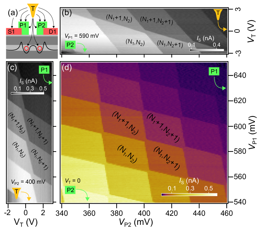
As sketched in Fig. 3a, the tip is coupled almost symmetrically to both sides of the DQD. However, depending on the specific tuning of (,), the tip can locally serve as a plunger gate for each dot. In Figs. 3b - d we plot charge stability diagrams acquired by sweeping different pairs of gates, while keeping the other gate fixed. We keep the position of the tip close to the center of the circle in Fig. 2e. All three data sets exhibit standard DQD charge stability diagrams 43. From these data, we extract the capacitance matrix from (in units of ):
| (1) |
As expected from the gate geometry, the diagonal elements in the left block are a few times larger than the off-diagonal elements and a few orders of magnitude larger than tip-to-dot capacitances. The tip-to-dot capacitances are small due to the fact that the region of the 2DEG exposed to the electric field from the tip is only and the rest of the electric field is screened by metallic gates as indicated in Fig. 3a.
Despite its small lever arm, we can drive PAT transitions by applying a microwave tone to the tip 39, 44. PAT can be used to probe the energy level structure of the DQD, as we now demonstrate. Figure 4a illustrates the PAT process at negative detuning and with a fixed . A photon () or a pair of photons () incident from the tip drives the current through the DQD as the electron jumps from the ground state in the right dot to either the ground or excited state in the left dot. At positive detuning the process is similar but photon absorption is replaced by emission 45.
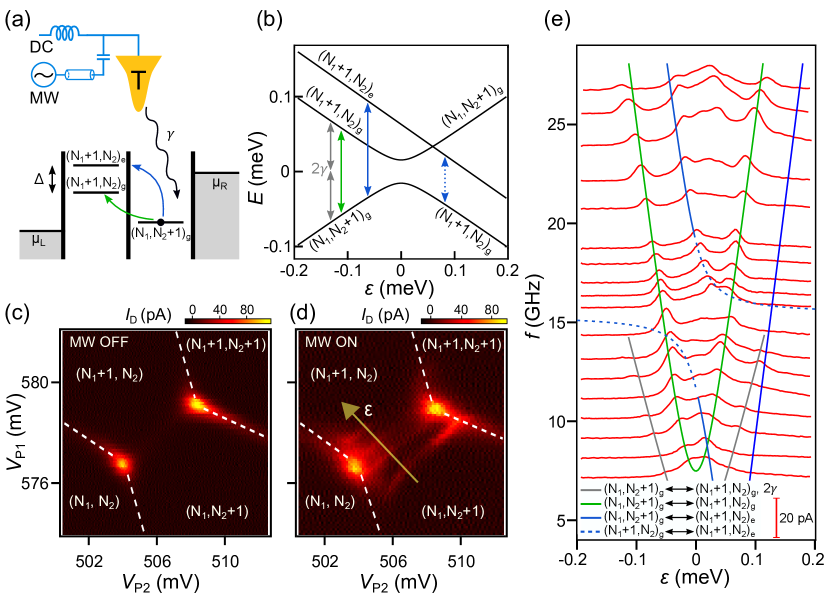
The contribution of PAT processes to is shown in Figs. 4c,d. With the microwave drive on (Fig. 4d) stripes of a finite current appear in the region between triple points where resonant tunneling is normally prohibited (Fig. 4c). We define the detuning axis as being perpendicular to the PAT stripes as highlighted by a yellow arrow in Fig. 4d. The evolution of linecuts is shown in Fig. 4e as a function of microwave frequency . Here we plot , averaged over a range of microwave powers, as a function of and spaced in accordance to microwave frequency since at large detuning. For , the PAT peaks are symmetric around and shift to larger detuning with increasing photon frequency, consistent with a simple two level model of a charge qubit 44. However, for , an additional PAT peak emerges. We fit these data using a three level Hamiltonian similar to a model that includes a higher-lying valley state in one of the dots40. It includes the right dot ground state , the left dot ground state , and the left dot excited state , as shown in Fig. 4b. The anti-crossing between ground states is governed by , where is Planck’s constant and is the interdot tunnel coupling39. Calculated transition frequencies are plotted in Fig. 4e along with . We obtain best fit values of and an excited state energy . Note that the transition is not visible at large detuning since the intradot transition does not contribute to the net current. Also the transition is not visible at large positive detuning as the population of the excited state is suppressed at low temperatures. Finally, we note that a value of is consistent with valley splittings reported in the literature25, 18, 19, 17.
2.1 Conclusion
In conclusion, we demonstrated coupling between a lithographically defined DQD in a Si/SiGe heterostructure and the tip of a tuning fork based AFM. We performed manipulation and imaging of single electrons inside the DQD by means of transport and charge sensing measurements. Furthermore, we quantitatively characterized the tip-device interactions by means of the capacitance matrix, illustrating how the tip can be used as a local plunger gate to tune the electron occupancy in the DQD. By applying microwave signals to the tip, we were able to drive PAT events and perform excited state spectroscopy. Our experiments demonstrate local microscope-based dc and microwave control of a DQD - the standard building block for semiconductor quantum devices. Our work is also a starting point for spatially resolved excited state spectroscopy, which may allow us to map the variation of valley splitting in Si/SiGe heterostructures.
Supported by Army Research Office grant W911NF-15-1-0149 and the Gordon and Betty Moore Foundation’s EPiQS Initiative through Grant No. GBMF4535. The authors thank F. F. L. Borjans for technical contributions to device fabrication and HRL Laboratories for providing the Si/SiGe heterostructures.
References
- Nielsen and Chuang 2010 Nielsen, M. A.; Chuang, I. L. Quantum Computation and Quantum Information: 10th Anniversary Edition. 2010,
- Kjaergaard et al. 2020 Kjaergaard, M.; Schwartz, M. E.; Braumüller, J.; Krantz, P.; Wang, J. I.-J.; Gustavsson, S.; Oliver, W. D. Superconducting Qubits: Current State of Play. Annu. Rev. Condens. Matter Phys. 2020, 11, 369–395
- Petersson et al. 2010 Petersson, K. D.; Petta, J. R.; Lu, H.; Gossard, A. C. Quantum Coherence in a One-Electron Semiconductor Charge Qubit. Phys. Rev. Lett. 2010, 105, 246804
- Nichol et al. 2015 Nichol, J. M.; Harvey, S. P.; Shulman, M. D.; Pal, A.; Umansky, V.; Rashba, E. I.; Halperin, B. I.; Yacoby, A. Quenching of dynamic nuclear polarization by spin–orbit coupling in GaAs quantum dots. Nat. Commun. 2015, 6, 7682
- Loss and DiVincenzo 1998 Loss, D.; DiVincenzo, D. P. Quantum computation with quantum dots. Phys. Rev. A 1998, 57, 120–126
- Zwanenburg et al. 2013 Zwanenburg, F. A.; Dzurak, A. S.; Morello, A.; Simmons, M. Y.; Hollenberg, L. C. L.; Klimeck, G.; Rogge, S.; Coppersmith, S. N.; Eriksson, M. A. Silicon quantum electronics. Rev. Mod. Phys. 2013, 85, 961–1019
- Zajac et al. 2015 Zajac, D. M.; Hazard, T. M.; Mi, X.; Wang, K.; Petta, J. R. A reconfigurable gate architecture for Si/SiGe quantum dots. Appl. Phys. Lett. 2015, 106, 223507
- Zajac et al. 2016 Zajac, D. M.; Hazard, T. M.; Mi, X.; Nielsen, E.; Petta, J. R. Scalable Gate Architecture for a One-Dimensional Array of Semiconductor Spin Qubits. Phys. Rev. Applied 2016, 6, 054013
- Tyryshkin et al. 2012 Tyryshkin, A. M.; Tojo, S.; Morton, J. J. L.; Riemann, H.; Abrosimov, N. V.; Becker, P.; Pohl, H.-J.; Schenkel, T.; Thewalt, M. L. W.; Itoh, K. M.; Lyon, S. A. Electron spin coherence exceeding seconds in high-purity silicon. Nat. Mater. 2012, 11, 143–147
- Mills et al. 2021 Mills, A. R.; Guinn, C. R.; Gullans, M. J.; Sigillito, A. J.; Feldman, M. M.; Nielsen, E.; Petta, J. R. Two-qubit silicon quantum processor with operation fidelity exceeding 99. arXiv:2111.11937 2021,
- Xue et al. 2022 Xue, X.; Russ, M.; Samkharadze, N.; Undseth, B.; Sammak, A.; Scappucci, G.; Vandersypen, L. M. K. Quantum logic with spin qubits crossing the surface code threshold. Nature 2022, 601, 343–347
- Noiri et al. 2022 Noiri, A.; Takeda, K.; Nakajima, T.; Kobayashi, T.; Sammak, A.; Scappucci, G.; Tarucha, S. Fast universal quantum gate above the fault-tolerance threshold in silicon. Nature 2022, 601, 338–342
- Weinstein et al. 2022 Weinstein, A. J. et al. Universal logic with encoded spin qubits in silicon. arXiv:2202.03605 2022,
- Friesen and Coppersmith 2010 Friesen, M.; Coppersmith, S. N. Theory of valley-orbit coupling in a Si/SiGe quantum dot. Phys. Rev. B 2010, 81, 115324
- Buterakos and Sarma 2021 Buterakos, D.; Sarma, S. D. Spin-Valley Qubit Dynamics In Exchange Coupled Silicon Quantum Dots. PRX Quantum 2021, 2, 040358
- Schäffler 1997 Schäffler, F. High-mobility Si and Ge structures. Semicond. Sci. Technol. 1997, 12, 1515–1549
- Goswami et al. 2007 Goswami, S.; Slinker, K. A.; Friesen, M.; McGuire, L. M.; Truitt, J. L.; Tahan, C.; Klein, L. J.; Chu, J. O.; Mooney, P. M.; van der Weide, D. W.; Joynt, R.; Coppersmith, S. N.; Eriksson, M. A. Controllable valley splitting in silicon quantum devices. Nat. Phys. 2007, 3, 41–45
- Borjans et al. 2021 Borjans, F.; Zhang, X.; Mi, X.; Cheng, G.; Yao, N.; Jackson, C.; Edge, L.; Petta, J. Probing the Variation of the Intervalley Tunnel Coupling in a Silicon Triple Quantum Dot. PRX Quantum 2021, 2, 020309
- Mi et al. 2017 Mi, X.; Péterfalvi, C. G.; Burkard, G.; Petta, J. R. High-Resolution Valley Spectroscopy of Si Quantum Dots. Phys. Rev. Lett. 2017, 119, 176803
- Borjans et al. 2019 Borjans, F.; Zajac, D. M.; Hazard, T. M.; Petta, J. R. Single-Spin Relaxation in a Synthetic Spin-Orbit Field. Phys. Rev. Applied 2019, 11, 044063
- Tariq and Hu 2019 Tariq, B.; Hu, X. Effects of interface steps on the valley-orbit coupling in a Si/SiGe quantum dot. Phys. Rev. B 2019, 100, 125309
- Culcer et al. 2010 Culcer, D.; Hu, X.; Das Sarma, S. Interface roughness, valley-orbit coupling, and valley manipulation in quantum dots. Phys. Rev. B 2010, 82, 205315
- Jiang et al. 2012 Jiang, Z.; Kharche, N.; Boykin, T.; Klimeck, G. Effects of interface disorder on valley splitting in SiGe/Si/SiGe quantum wells. Appl. Phys. Lett. 2012, 100, 103502
- Neyens et al. 2018 Neyens, S. F.; Foote, R. H.; Thorgrimsson, B.; Knapp, T. J.; McJunkin, T.; Vandersypen, L. M. K.; Amin, P.; Thomas, N. K.; Clarke, J. S.; Savage, D. E.; Lagally, M. G.; Friesen, M.; Coppersmith, S. N.; Eriksson, M. A. The critical role of substrate disorder in valley splitting in Si quantum wells. Appl. Phys. Lett. 2018, 112, 243107
- Borselli et al. 2011 Borselli, M. G.; Ross, R. S.; Kiselev, A. A.; Croke, E. T.; Holabird, K. S.; Deelman, P. W.; Warren, L. D.; Alvarado-Rodriguez, I.; Milosavljevic, I.; Ku, F. C.; Wong, W. S.; Schmitz, A. E.; Sokolich, M.; Gyure, M. F.; Hunter, A. T. Measurement of valley splitting in high-symmetry Si/SiGe quantum dots. Appl. Phys. Lett. 2011, 98, 123118
- Ferdous et al. 2018 Ferdous, R.; Kawakami, E.; Scarlino, P.; Nowak, M. P.; Ward, D. R.; Savage, D. E.; Lagally, M. G.; Coppersmith, S. N.; Friesen, M.; Eriksson, M. A.; Vandersypen, L. M. K.; Rahman, R. Valley dependent anisotropic spin splitting in silicon quantum dots. npj Quantum Inf. 2018, 4, 26
- Hollmann et al. 2020 Hollmann, A.; Struck, T.; Langrock, V.; Schmidbauer, A.; Schauer, F.; Leonhardt, T.; Sawano, K.; Riemann, H.; Abrosimov, N. V.; Bougeard, D.; Schreiber, L. R. Large, Tunable Valley Splitting and Single-Spin Relaxation Mechanisms in a / Quantum Dot. Phys. Rev. Applied 2020, 13, 034068
- Chen et al. 2021 Chen, E. H. et al. Detuning Axis Pulsed Spectroscopy of Valley-Orbital States in /- Quantum Dots. Phys. Rev. Applied 2021, 15, 044033
- Shim et al. 2019 Shim, Y.-P.; Ruskov, R.; Hurst, H. M.; Tahan, C. Induced quantum dot probe for material characterization. Appl. Phys. Lett. 2019, 114, 152105
- Pioda et al. 2004 Pioda, A.; Kičin, S.; Ihn, T.; Sigrist, M.; Fuhrer, A.; Ensslin, K.; Weichselbaum, A.; Ulloa, S. E.; Reinwald, M.; Wegscheider, W. Spatially Resolved Manipulation of Single Electrons in Quantum Dots Using a Scanned Probe. Phys. Rev. Lett. 2004, 93, 216801
- Huefner et al. 2011 Huefner, M.; Kueng, B.; Schnez, S.; Ensslin, K.; Ihn, T.; Reinwald, M.; Wegscheider, W. Spatial mapping and manipulation of two tunnel-coupled quantum dots. Phys. Rev. B 2011, 83, 235326
- Fallahi et al. 2005 Fallahi, P.; Bleszynski, A. C.; Westervelt, R. M.; Huang, J.; Walls, J. D.; Heller, E. J.; Hanson, M.; Gossard, A. C. Imaging a Single-Electron Quantum Dot. Nano Lett. 2005, 5, 223–226
- Woodside and McEuen 2002 Woodside, M. T.; McEuen, P. L. Scanned Probe Imaging of Single-Electron Charge States in Nanotube Quantum Dots. Science 2002, 296, 1098–1101
- Bleszynski-Jayich et al. 2008 Bleszynski-Jayich, A. C.; Fröberg, L. E.; Björk, M. T.; Trodahl, H. J.; Samuelson, L.; Westervelt, R. M. Imaging a one-electron InAs quantum dot in an InAs/InP nanowire. Phys. Rev. B 2008, 77, 245327
- Gildemeister et al. 2007 Gildemeister, A. E.; Ihn, T.; Schleser, R.; Ensslin, K.; Driscoll, D. C.; Gossard, A. C. Imaging a coupled quantum dot-quantum point contact system. J. Appl. Phys. 2007, 102, 083703
- Zajac et al. 2018 Zajac, D. M.; Sigillito, A. J.; Russ, M.; Borjans, F.; Taylor, J. M.; Burkard, G.; Petta, J. R. Resonantly driven CNOT gate for electron spins. Science 2018, 359, 439–442
- Burkard et al. 2021 Burkard, G.; Ladd, T. D.; Nichol, J. M.; Pan, A.; Petta, J. R. Semiconductor Spin Qubits. arXiv:2112.08863 2021,
- Oh et al. 2021 Oh, S. W.; Denisov, A. O.; Chen, P.; Petta, J. R. Cryogen-free scanning gate microscope for the characterization of Si/Si0.7Ge0.3 quantum devices at milli-Kelvin temperatures. AIP Adv. 2021, 11, 125122
- van der Wiel et al. 2002 van der Wiel, W. G.; De Franceschi, S.; Elzerman, J. M.; Fujisawa, T.; Tarucha, S.; Kouwenhoven, L. P. Electron transport through double quantum dots. Rev. Mod. Phys. 2002, 75, 1–22
- Wang et al. 2013 Wang, K.; Payette, C.; Dovzhenko, Y.; Deelman, P. W.; Petta, J. R. Charge Relaxation in a Single-Electron Double Quantum Dot. Phys. Rev. Lett. 2013, 111, 046801
- Khrapai et al. 2006 Khrapai, V. S.; Ludwig, S.; Kotthaus, J. P.; Tranitz, H. P.; Wegscheider, W. Double-Dot Quantum Ratchet Driven by an Independently Biased Quantum Point Contact. Phys. Rev. Lett. 2006, 97, 176803
- 42 Supplemental Material
- Hanson et al. 2007 Hanson, R.; Kouwenhoven, L. P.; Petta, J. R.; Tarucha, S.; Vandersypen, L. M. K. Spins in few-electron quantum dots. Rev. Mod. Phys. 2007, 79, 1217–1265
- Petta et al. 2004 Petta, J. R.; Johnson, A. C.; Marcus, C. M.; Hanson, M. P.; Gossard, A. C. Manipulation of a Single Charge in a Double Quantum Dot. Phys. Rev. Lett. 2004, 93, 186802
- Oosterkamp et al. 1998 Oosterkamp, T. H.; Fujisawa, T.; van der Wiel, W. G.; Ishibashi, K.; Hijman, R. V.; Tarucha, S.; Kouwenhoven, L. P. Microwave spectroscopy of a quantum-dot molecule. Nature 1998, 395, 873–876