Optically coherent nitrogen-vacancy defect centers in diamond nanostructures
Abstract
Optically active solid-state spin defects have the potential to become a versatile resource for quantum information processing applications. Nitrogen-vacancy defect centers (NV) in diamond act as quantum memories and can be interfaced by coherent photons as demonstrated in entanglement protocols. However, in particular in diamond nanostructures, the effect of spectral diffusion leads to optical decoherence hindering entanglement generation. In this work, we present strategies to significantly reduce the electric noise in diamond nanostructures. We demonstrate single NVs in nanopillars exhibiting lifetime-limited linewidth on the time scale of one second and long-term spectral stability with inhomogeneous linewidth as low as 150 MHz over three minutes. Excitation power and energy-dependent measurements in combination with nanoscopic Monte Carlo simulations contribute to a better understanding of the impact of bulk and surface defects on the NV’s spectral properties. Finally, we propose an entanglement protocol for nanostructure-coupled NVs providing entanglement generation rates up to hundreds of kHz.
I I. Introduction
Optically active solid-state spin defects form a resource for a variety of quantum applications, including sensing [1], secure communication [2, 3], and information processing applications [4, 5]. In many proposed quantum repeater protocols, quantum information transfer is achieved by interfacing spin qubits with photons [6, 7, 8, 9]. Prominently, the negatively charged nitrogen-vacancy defect center (NV) in diamond has enabled spin-photon and subsequent spin-spin entanglement of distant qubits [10, 11], recently even for a three-node quantum network [12]. However, all these impressive experiments have been performed with NVs in bulk samples using solid immersion lenses [13] that are relatively inefficient photonic structures compared to nanostructures [14]. Nanostructures have enabled high photon detection rates [15, 16], more efficient fibre coupling [17, 18], increased light-matter interaction [19], and allow for photonic integration [20]. These improvements are crucial requirements for further quantum technology development, but to date NVs in any nanostructure have not yet enabled the generation of coherent single photon states, which are the basis of any entanglement protocol. Lifetime-limited optical transition linewidths for NVs in nanostructures are hindered by the effect of spectral diffusion [21, 22, 23]. Defects in the vicinity of the NV act as charge traps and electron donors that can be photoionized, inducing electromagnetic noise and a fluctuating DC Stark shift of the optical transition frequency over time as illustrated in Fig. 1a. While in bulk samples NVs with almost lifetime-limited optical linewidth of 27 MHz have been demonstrated [24], in nanostructures the linewidth is inhomogeneously broadened to hundreds of MHz or even several GHz [20, 22, 25]. The NV charge environment depends strongly on the material properties and fabrication process, i.e. NV formation, defect density, and diamond structuring methods, as well as the distance of the NV to the surface. In recent works, it was shown that narrow linewidth NVs can be found predominantly for NVs formed from native nitrogen rather than for NVs created by ion implantation, which introduces local lattice damage such as vacancies [26, 27]. For shallow NVs, surface defects are considered the main source of charge noise [28]. Although significant efforts have been made over the past decade, the development of nanofabrication techniques [29, 30] and surface termination [31] for improved material quality as well as active control schemes [32] have not yet been able to sufficiently prevent spectral diffusion in diamond nanostructures.
Here, we investigate the spectral properties of natural single NVs incorporated in diamond nanostructures with radii of 125 nm by performing photoluminescence excitation (PLE) spectroscopy. We systematically examine spectral diffusion in three different excitation regimes: (1) red continuous wave (CW) illumination, (2) two-color excitation with red and higher energetic laser light, as well as (3) a shutter experiment where the NV is excited after periods of darkness. All three regimes are relevant for prospective quantum applications, for example, entanglement generation. We identify key parameters in control schemes for preserving spectral stability on a time scale of minutes. Furthermore, the comparison of experimental results with nanoscopic Monte Carlo simulations reveals the relation of spectral diffusion dynamics to the type and number of ionized defects. In the presented system, both bulk and surface defects contribute to an overall linewidth broadening. Finally, we propose a control protocol for efficient entanglement generation using NVs coupled to nanostructures based on the findings of this paper.
II II. Sample
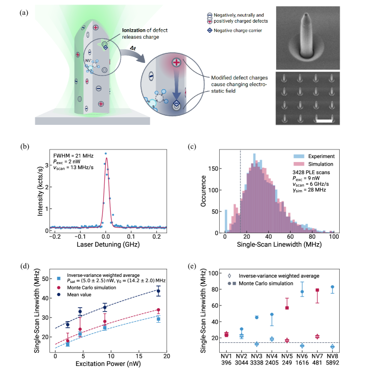
In contrast to most previous investigations, we select a commercial chemical vapor deposition grown sample with a relatively high density of 1 ppm nitrogen atoms [33] resulting in a density of roughly 10 ppb NV defect centers and a suitable yield in our NV-nanostructure device fabrication of about 10%. Nanopillar fabrication of the -oriented single-crystalline diamond substrate was carried out with dry etching processes [34] (Appendix A). The parameters of each step have been optimized to minimize the structural damage of the diamond surface, thus enabling repeatable high-quality fabrication over large areas as evident in the scanning electron microscopy images in Fig. 1a. The nanopillar radii of 125 nm are optimized for photon coupling and the height of 1.6 µm allows for the optical separation of nanopillar NVs from bulk NVs.
III III. Single-Scan Linewidth
The linewidth of the NV zero-phonon line (ZPL) is investigated at temperatures below 4 K by PLE spectroscopy. Here, the frequency of the excitation laser is tuned across the ZPL at 637 nm and the photons emitted in the phonon-sideband (650-800 nm) are detected. Single-scan linewidths reveal information about the indistinguishability of emitted photons. The data in Fig. 1b demonstrate lifetime-limited linewidth of a single NV embedded in a diamond nanostructure for scan speeds as slow as approximately one natural linewidth per second and for excitation powers of half of the saturation power ( nW, see Supplemental Material for further details [35]). While this PLE scan is post-selected, we also statistically analyse the NV linewidth at different scan speeds and laser powers by performing thousands of PLE scans. Individual linewidths are fitted by a Voigt profile and the characteristic single-scan linewidth of a data set is determined by using the inverse-variance weighting method and a new evaluation method based on Monte Carlo simulations that we introduce in this work (Appendix B). Due to a low number of detection events per time bin at fast scan speeds, the recorded spectra not only display a large distribution of linewidths, but produce also unphysically narrow lines below the lifetime-limited linewidth (Fig. 1c). This discrepancy does not allow for a direct analysis of the linewidth via simple averaging or weighting of the data, a challenge that also applies to previous works. To address this problem we employ a Monte Carlo simulation: Cauchy distributed detection events and noise are fitted with a Voigt profile. The resulting linewidths are summarized in a histogram. We then use a -test to find the best linewidth corresponding to the measured data.
Excitation power-dependent measurements (Fig. 1d) allow for finding a parameter regime in which the spectral stability and the negative charge state are preserved for long times while still a large number of photons are emitted. For a scan speed of 6 GHz/s the effect of power broadening limits the preservation of lifetime-limited linewidth on average which is extracted to be () MHz for zero excitation power. Comparing standard data analysis methods with our Monte Carlo approach, we find a significant offset for the mean value and only a small deviation by applying the inverse-variance weighting method. However, for faster scan speeds, linewidths determined with both previously used methods are prone to non-negligible errors (Fig. 1e).
The observed NV properties can be similarly reproduced with NVs in other nanopillars. We investigate two sample regions containing in total 180 nanopillars. Of these, about 10 contain single NVs, i.e. appear bright in PL scans. Finally, we measure a PLE signal of eight single NVs in different nanopillars, exhibiting overall narrow linewidths with an extracted single-scan linewidth ranging from close to the lifetime-limit to about a 6-fold broadening of 83 MHz (Fig. 1e). For this overview measurement, we apply, in contrast to the other measurements, a green re-pump pulse before every line scan to ensure initialization into the negative NV charge state, leading to an additional broadening of the single-scan linewidth compared to Fig. 1d. All subsequent results presented in this work stem from characterization of NV3.
IV IV. Inhomogeneous Linewidth and Ionization Time
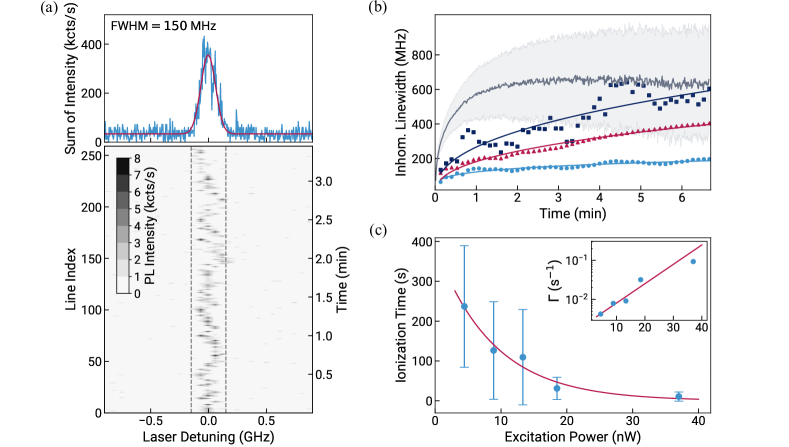
Besides single-scan linewidths, which determine photon coherence on short time scales, the inhomogeneous linewidth of single NVs is an important figure of merit for the performance of quantum entanglement protocols. In this section we investigate the inhomogeneous linewidth over a time scale of several minutes. After preparing the NV in the negative charge state by using a green initialization pulse, hundreds of consecutive PLE scans are recorded at 2 nW (half of the saturation power) without reinitialization (Regime 1). Fig. 2a shows an example of a range of about 250 PLE scans and the summed PL intensity recorded on a time scale of more than three minutes. The process of spectral diffusion, in which the transition frequency randomly shifts in time, can be clearly seen in the bottom of Fig. 2a. The sum of intensities of the individual scans constitutes an inhomogeneously broadened linewidth of about 150 MHz, only an 11-fold broadening compared to the natural linewidth (top of Fig. 2a). Although the trajectory presented here is post-selected and is not representing the average inhomogeneous linewidth, we demonstrate that under suitable fabrication and control conditions remarkably narrow linewidth can be preserved for minutes in diamond nanostructures. In Fig. 2b, the time evolution of the inhomogeneous linewidth is shown. The FWHM of the inhomogeneous line is determined from a set of trajectories summing the respective intensities for a given time of up to seven minutes, corresponding to 500 consecutive PLE scans. The data include the trajectory shown in Fig. 2a (blue circles) as well as the averaged values of equivalent post-selected data sets (red triangles), and the results from all measured data sets (dark blue squares). As a post-selection criterion, we reject trajectories exhibiting a spectral jump which causes a line-to-line increase of more than 200 MHz of the cumulatively summed inhomogeneous linewidth. In 28 of the measured data, the NV is spectrally stable (400 MHz) and remains in its negative charge state for seven minutes while PLE scans are performed. A power law fit indicates that the phenomenon of spectral diffusion induced by resonant laser irradiation is an anomalous diffusion process, more precisely a subdiffusive process [36]. Additionally, we use a simple stochastic process (Wiener process, Appendix C) to model the spectral diffusion of the ZPL resonance. We also implemented the Ornstein-Uhlenbeck-model, but both approaches fail to reproduce the observed evolution of the inhomogeneous linewidth, confirming our conclusion that for the investigated system and chosen excitation parameters spectral diffusion is likely not characterized by a normal diffusion process.
In addition to spectral diffusion, charge state stability has been a challenge for NVs in nanostructures [20]. For investigating the ionization time, i.e. the time until the NV converts from the negative to the neutral charge state, we use again a PLE excitation scheme. The NV ZPL transition is driven about 0.2 of the time (duty cycle). The ionization time decays exponentially as a function of excitation power (Fig. 2c). At excitation powers on the order of the saturation power of 5 nW the ionization time is several minutes. During this time no green laser pulse needs to be applied for reinitializing the system, resulting in a significantly reduced spectral diffusion as evaluated in the following section.
V V. Spectral Diffusion Dynamics
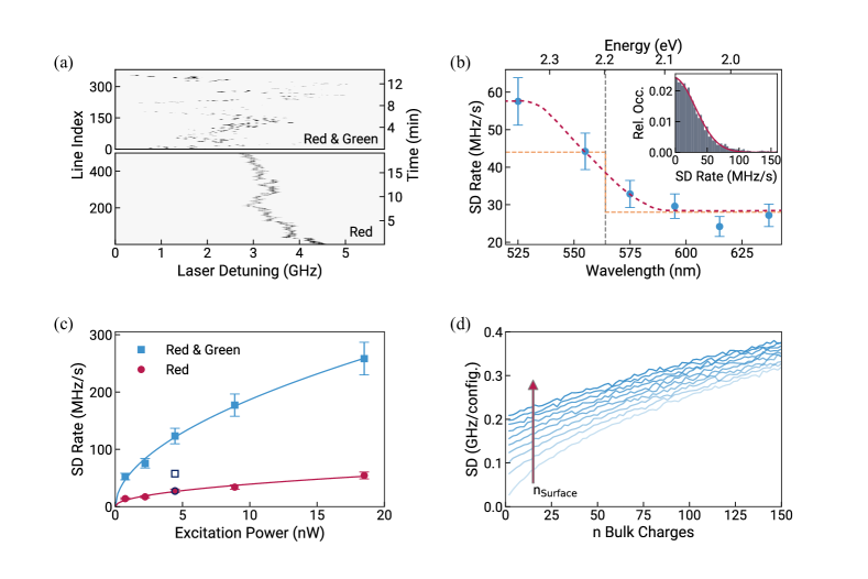
Although we have found comparatively long NV ionization times, occasionally the system ionizes. For the charge state conversion from NV0 to NV-, off-resonant excitation at 510 to 593 nm [37] as well as energies resonant to the NV0 transition at 575 nm [38] have been used, leading to different reinitialization efficiencies. Compared to 637 nm, the higher laser energies cause ionization of additional diamond impurities and charge dynamics which in turn lead to increased spectral diffusion, strongly reducing the optical coherence of NV defects [25]. While in PLE scans with only resonant laser light (Regime 1, see above) a relatively slow drift of the ZPL resonance over time is observed, two-color excitation using a mixture of resonant and green laser light (Regime 2) causes large spectral jumps of the ZPL resonance far exceeding the natural linewidth as shown in Fig. 3a. This is not surprising, since the sample exhibits a high intrinsic concentration of nitrogen bulk impurities, whose ionization energies are above 637 nm but below 525 nm. Moreover, higher laser energies also enable activation of additional surface defects inducing further charge noise.
To date the effect of non-resonant laser irradiation on spectral diffusion of a spectrally stable NV in a nanostructure has not been investigated systematically. We therefore examine energy-dependent spectral diffusion by applying a two-color excitation scheme, using 637 nm in combination with lower wavelength (higher energy) laser light ranging from 525 to 615 nm, and compare it to resonant single-color PLE scans. As characteristic quantity, we examine the spectral diffusion rate which is determined as the difference of resonance center frequencies in consecutive line scans normalized by the time step between each scan. In the two-color excitation experiment, we observe a significant increase of the spectral diffusion rate at wavelengths of 555 nm (2.23 eV) and lower (Fig. 3b). Above 555 nm, the relatively low spectral diffusion could be caused by ionization of the relatively few lattice vacancies (GR1, 1.67 eV) [39], defect states based on hydrogen (1.2 eV) [40], or rare boron defects (0.37 eV) [41] in bulk. Below 555 nm, the much stronger spectral diffusion is linked to the ionization of numerous nitrogen C-centers (2.20 eV)[40] and a variety of surface defects that are not identified individually (see below).
While energy-dependent measurements reveal the type of defect contributing to spectral diffusion, investigating the excitation power dependence provides insights into the number of defects. We find an approximate square root power law describing the increase of the spectral diffusion rate as a function of excitation power for both, one- and two-color excitation, where the magnitude of the spectral diffusion rate is significantly higher for excitation with additional green laser light (Fig. 3c). This functional relationship is qualitatively confirmed by modelling the impact of a fluctuating charge environment on the NV ZPL resonance with a Monte Carlo simulation (Fig. 3d, Appendix D). For the simulation the NV is placed in the center of a cylindrical volume with the same dimensions as the investigated nanopillars and is surrounded by randomly distributed charge traps at a density of 1 ppm according to the density of C-centers. In many iterations a fixed number of positive and negative charges are randomly distributed among the charge traps, representing the change of the charge environment during repeated line scans. A comparison of experiment and simulations indicates that there is a direct correlation between laser power and number of charges participating in the process.
Further insights into the contribution of bulk and surface defects are gained by comparing the sample after ten weeks at cryogenic temperatures and directly after a warm-up and a second cool-down. Remarkably, the overall excellent spectral properties of the investigated NV were preserved. Moreover, a comparison of the spectral diffusion rates produced by the two-color excitation at 525 nm with a power of 4 nW before the second cool-down with the corresponding values after the second cool-down reveals a significant reduction, whereas the spectral diffusion rate for resonant excitation remains similar (Fig. 3c). Although changes of the defect formation in the bulk crystal are possible, we suppose it is far more likely that the warm-up led to a release of non-ubiquitous surface defects, e.g. a layer of ice that had build up over time. Our simulations support this idea: For low excitation powers the number of participating bulk charges is relatively small. The impact of surface charges in this regime is much more pronounced and can cause a manyfold increase of the spectral diffusion rate as shown in Fig. 3d.
VI VI. NV in the Dark
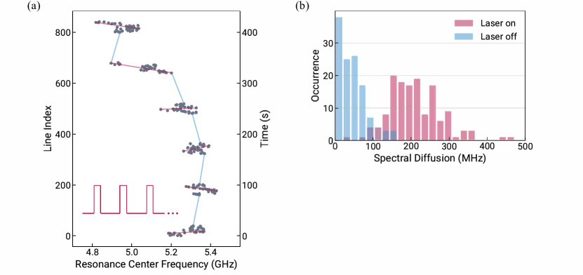
In previously demonstrated entanglement protocols, NVs were not exposed to laser light permanently, but resonant single-shot excitation pulses of the ZPL transitions were applied. To investigate the influence of spectral diffusion in nanostructures during darkness (Regime 3), we perform a shutter experiment. Here, the defect is exposed to resonance-scanning laser irradiation of 2 nW for 20 seconds and kept in darkness for 60 seconds in alternation without using green re-pump pulses (Fig. 4a, Appendix E). The frequency difference of the ZPL resonances before and after darkness, which would correspond to the difference of two single-shot read-out events, is on average 40 MHz and the main occurrence is about 10 MHz as summarized in the histogram in Fig. 4b. This measurement shows that without laser irradiation spectral diffusion is strongly reduced.
VII VII. Towards Entanglement Protocols
All previous long-distance spin-spin entanglement experiments [10, 11, 12] were demonstrated with NVs embedded in solid immersion lenses, which are bulk-like microstructures that maintain optical coherence, but provide limited NV to fibre coupling efficiencies. Entanglement attempt rates as large as 182 kHz and successful deterministic entanglement delivery at 10 Hz were demonstrated [11]. Nanostructures could potentially enhance the performance: improved design parameters enable for enhanced photon collection efficiencies [16, 17, 18] and increased light-matter interaction in the form of Purcell enhancement can be achieved [42, 19, 43, 22]. Considering the findings of our work, it might be possible to apply nanostructure embedded NVs for the generation of entanglement. To quantify the potential advantage, we adapt the established entanglement protocols based on -pulse excitation to the specific requirements of our NV-nanostructure system. In particular, we analyze the protocol with respect to the three investigated excitation regimes that represent the different laser control regimes in entanglement generation, namely, (1) resonant excitation, (2) higher energetic laser irradiation for initialization, and (3) dark diffusion.
We determine resonant -pulse parameters for the investigated NV of a duration of 2 ns and a peak power of 3 µW, which is technically easy to achieve (see Supplemental Material for further details [35]). From the spectral diffusion power law fit (Fig. 3c), we extract a spectral diffusion rate of 640 MHz/s during excitation pulses and use this value as an input parameter in a simple stochastic model of the spectral diffusion process to evaluate the coherence of the emitted photons (Appendix F). We assume that the inhomogeneous linewidth is bounded by the diffusion law , where is the spectral diffusion rate and the evolution time. Based on this diffusion law, we derive the number of entanglement attempts, i.e. -pulse excitations, that can be applied until the line is broadened by a certain amount. For example, an inhomogeneous broadening of 1 is a relevant regime as it still enables a Hong-Ou-Mandel visibility of around 90 and an entanglement fidelity for creating a photonic Bell-state with an optical circuit of up to 87 which we extract from ref. [44].
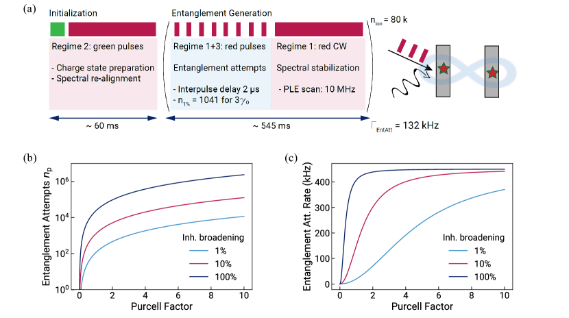
Independent of the type of nanostructure, the NV’s spectral properties are assumed to be similar as presented in this work when the NV is located with at least 125 nm distance to the surface. Considering an optical nanocavity, Purcell enhancement leads to a lifetime reduction and consequently to a broadening of the homogeneous linewidth [19]. According to our stochastic model, for a fixed spectral diffusion rate a broadening of the homogeneous linewidth allows for more entanglement attempts that can be applied while optical coherence is maintained (Fig. 5b). Assuming a three-fold broadening of the natural linewidth, we expect to make 1041 entanglement attempts until the total linewidth is broadened by . Based on this result, we propose a control protocol for NVs in different types of nanostructures, taking into account the average time it takes for steady spectral re-alignment as well as system preparation after reinitialization based on PLE scans and Stark tuning [45] (Fig. 5a, Appendix F). Entanglement attempt rates ranging from 20 kHz up to 450 kHz can be achieved, considering the present system with a Purcell factor set to one and other types of nanostructures that provide larger Purcell enhancement (Fig. 5c). Here, the maximum entanglement rate is limited by the entanglement attempt duration of 2 µs adapted from ref. [11] and system preparation time after ionization, that could both be technically improved.
Besides reducing the sensitivity to spectral diffusion, resonant nanostructures can significantly increase the successful entanglement delivery rate by optimized fibre-coupling. In previous work, a coupling of of NV emission into a cavity mode was demonstrated together with a 2.7-fold Purcell enhancement [19]. It was also shown that diamond cavity photons can be fiber-coupled and detected with an overall system efficiency of 85 [46]. Combining these achievements we expect for a cavity-coupled NV that of all photons are emitted into the ZPL and fibre-coupled for entanglement generation. An enhancement in ZPL emission and photon collection efficiency by more than two orders of magnitude would enable appropriate entanglement delivery rates up to hundreds of kHz.
VIII VIII. Conclusion
In this article, we demonstrated spectrally stable NVs in diamond nanostructures enabled by a combination of methods ranging from selection of material properties, suitable fabrication recipes, to specific control schemes. The choice of a substrate providing natural NVs and careful use of established fabrication methods facilitate reduced structural damage. We implemented sample specific control sequences, i.e. weak resonant excitation and reduction of high energy initialization pulses, maximally limiting charge noise. In this way, narrow inhomogeneous linewidth of the NV ZPL over minutes was demonstrated. The overall spectral stability was confirmed by recording a large number of trajectories, ensuring statistical significance of our findings. While one defect was investigated in detail, we identified seven other color centers with narrow single-scan linewidths. We performed a systematic characterization of the spectral diffusion of the NV ZPL resonance under different excitation regimes and investigated the contribution of bulk and surface defects by complementing the experimental results with a nanoscopic model. We suppose that our methods are applicable to any other nanostructure with natural NVs located about 125 nm apart from the surface. Therefore, a proposal of distributed NV-NV entanglement generation is presented, which can, taking advantage of increased photon collection efficiencies and Purcell enhancement in nanocavities, prospectively yield increased entanglement rates up to hundreds of kHz. In conclusion, we demonstrated a device based on a nanostructure-coupled NV with optical properties suitable for quantum coherent control protocols.
Appendix A Appendix A: Sample preparation
The nanostructures were fabricated on a commercially available -oriented single-crystalline diamond substrate, grown by chemical vapour deposition [33]. The sample surface is initially cleaned in a boiling tri-acid solution (1:1:1 of H2SO4 : HNO3 : HClO4) [47] and subsequently etched in Cl2- and O2-based plasmas in order to remove any organic contaminants and structural defects [48]. The fabrication process is similar to those presented in previous works [34]. After the deposition of a 200 nm-thick layer of Si3N4 in an inductively coupled-plasma (ICP) enhanced CVD system, the sample is spin-coated with 300 nm of electro-sensitive resist (ZEP520A) and patterned by e-beam lithography. After development, the pattern is transferred into the Si3N4 layer by a reactive ion etching process in a CF4-based plasma (10 sccm, RF Power 100 W, P 1 Pa) and subsequently etched into the diamond during an ICP process (O2, 80 sccm, ICP Power 750 W, RF Power 200 W, P 0.3 Pa). The sample is finally cleaned in a buffered-HF solution, which completely dissolves the Si3N4 layer and thus exposes the diamond surface. For more details the reader is referred to the Supplemental Material [35].
Appendix B Appendix B: Monte Carlo linewidth simulation
Fast spectral scans make it difficult to determine the homogeneous linewidth of an emitter because only a few photons are collected in a single scan. Our statistical analysis shows that fitting single-line scans with a Voigt profile, which involve fewer than 20 photons, will skew the main occurrence of linewidths towards unphysically narrow lines. To ameliorate this problem, we elected to use a Monte Carlo simulation of the line scan and fitting procedure allowing us to better determine the homogeneous linewidth of spectrally unstable emitters. A single iteration of the simulation contains the following steps: A number of detection events is drawn from a Poisson distribution with a fixed mean. The events are scattered along a fixed frequency interval, weighted by a Cauchy distribution with a fixed width . Additionally, a number of noise events is drawn from a Poisson distribution with a fixed mean and scattered along the frequency interval. The resulting spectrum is then fitted with a Voigt profile, and the resulting FWHM and fitting error is recorded. This is repeated for at least as many iterations as there are line scans in the experiment. We reject lines that have fewer than 5 photons in a frequency bin (4 MHz width). Crucially, the Monte Carlo simulation allows for a change in the mean number of photon detection events () and the linewidth of the Cauchy distribution. The linewidth statistics of the Monte Carlo simulation can then be used to determine both parameters, linewidth and average photon number, by comparing them with the experimental data. As in [49] we use a -test to determine a best estimate of the parameters. For more details the reader is referred to the Supplemental Material [35].
Appendix C Appendix C: Stochastic diffusion model
To determine the distribution of inhomogeneous linewidths we employ the following method: We repeatedly simulate 14 frequency trajectories whose diffusion dynamics are determined by a Wiener process. The inhomogeneous linewidth is found by fitting the trajectories at a given time step with a Voigt profile. This way we find the a distribution of inhomogeneous linewidths at a given time step. For each time step we can then calculate the mean and the variance as shown in Fig. 2b. For smaller times, the average linewidth evolution of the selected measured trajectories do not fall within one standard deviation of the simulated linewidths. This can either be attributed to the post selection or subdiffusive behaviour. For larger times the mean of the simulated trajectories deviates significantly from the square root behaviour expected for a normal diffusion process. This can be attributed to simulating only a few trajectories, which leads to large fluctuations in the fitting procedure. We also examined an Ornstein-Uhlenbeck process to model the diffusion of the spectral line. We could not find a good qualitative agreement between the Ornstein-Uhlenbeck process and the broadening of the spectral line for various drift parameters. For more details the reader is referred to the Supplemental Material [35].
Appendix D Appendix D: Monte Carlo Simulation of fluctuating electric field
The NV’s ZPL is sensitive to local electric fields due to the lack of inversion symmetry. A fluctuating charge environment produces a fluctuating local electric field at the position of the NV, which in turn Stark shifts the position of the emission line. The accumulation of these shifts over time results in an inhomogeneously broadened spectral line. In a single iteration of the Monte Carlo simulation we distribute a fixed number of charges in a volume that has the dimensions of the nano-pillars used in the experiment. We then determine the magnitude of the Stark shift by calculating the local electric field produced by the randomly arranged charges. For that we make use of the closed expression of the electric field produced by a point charge in a dielectric cylinder [50]. Charge screening is not systematically included in our simulations, possibly resulting in a quantitative overestimation of the accumulated local electric field fluctuations and spectral diffusion generated by a certain number of charges [51]. For more detail the reader is referred to the Supplemental Material [35].
Appendix E Appendix E: Shutter experiment
The laser is switched on and off by using a mechanical shutter while PLE scans are performed continuously. Since even weak laser irradiation during the PLE scans (a few hundred ms) induces spectral diffusion, we argue that for a -pulsed single-shot excitation on the nanosecond time scale spectral diffusion would be much more suppressed, if not fully absent.
Appendix F Appendix F: Entanglement protocol
We derive a quantitative estimate of the number of entanglement attempts (-pulse excitations) given a certain spectral diffusion rate that can be applied until the linewidth is broadened by a certain amount. We base our estimates on the Wiener process, which provides an upper bound estimation for the inhomogeneous linewidth broadening and thus a lower bound on the number of attempts. The time dependent FWHM of a Voigt profile which broadens in time due to a random walk of the frequency is given by
| (A1) |
where we used the approximation of the FWHM of a Voigt profile found in [52]. is the homogeneous linewidth and the inhomogeneous contribution is linked to the spectral diffusion rate by
| (A2) |
where is the time step for which was determined and is the time that has elapsed. The two constants are , . We can calculate the time it takes to broaden the line by percent of its original value []:
| (A3) |
The time is determined by the spectral diffusion rate corresponding to the -pulse power and the homogeneous linewidth of the emitter. We assume that between the -pulses, i.e. during darkness, spectral diffusion is not present. Hence, in a protocol based on single-shot excitation through -pulses with pulse duration , the number of entanglement attempts during the time is given by
| (A4) |
The entanglement protocol consists of three parts, namely NV initialization (charge state preparation and spectral tuning), entanglement generation, and spectral re-alignment. Entanglement generation is achieved by applying resonant -pulses with interpulse delays of 2 µs (repetition rate of 500 kHz) to the system. During a heralded single-photon entanglement generation attempt the spin state is prepared optically, a microwave pulse is used to create the superposition state and finally a resonant read-out -pulse generates spin–photon entanglement followed by an additional microwave -pulse [11]. After the estimated time during which an inhomogeneous linewidth broadening of percent is induced, a spectral re-alignment is performed. Here, the resonance is scanned in the vicinity ( MHz) of the target resonance frequency. The PLE scan is performed at a scan speed of 6 GHz/s resulting in a scan time of about 3.3 ms. Fitting the data and extracting the resonance center frequency would take less than 0.7 ms. Taking time for data processing and Stark tuning into account, we estimate a spectral re-alignment time of ms when no large spectral jumps occur. The number of entanglement attempts per ionization time of 545 ms, where entanglement generation schemes and spectral re-alignment protocols are applied alternating, is calculated by
| (A5) |
Here, corresponds to the entanglement attempt number multiplied with the -pulse separation time of 2 µs.
When the NV ionizes, it would be reinitialized by a 5 µs green re-pump pulse and tuned again into resonance ( ms). The high-energy initialization pulse likely causes a large spectral jump of the ZPL resonance within the inhomogeneous linewidth of 5 GHz. To localize the ZPL resonance after the initialization pulse, a PLE scan at a scan speed of 50 GHz/s is performed. On average it takes 50 ms for the tunable laser to reach the resonance and induce an increase in count rate that will be detected. When the photon number passes a threshold significantly exceeding the dark count rate the scan is stopped, the resonance would be localized, and a DC voltage applied for tuning the ZPL resonance to the target frequency. For spectral fine-tuning again the spectral re-alignment scheme with PLE scans in the vicinity of the ZPL resonance frequency would be applied.
The final entanglement attempt rate is determined by normalizing the number of entanglement attempts during the ionization time by the total protocol duration
| (A6) |
For increasing Purcell factors, a saturation of the entanglement attempt rate towards 450 kHz can be observed. The upper limit of entanglement attempt rate is given by the repetition rate of 500 kHz as well as the ratio of entanglement generation time and system preparation time. Here, the shown entanglement attempt rate is not limited by physical laws, but technical issues that can be improved. For more details on the estimation of -pulse parameters and the ionization time the reader is referred to the Supplemental Material [35].
Acknowledgments
The authors would like to thank J.H.D. Munns for helpful discussions and technical support in the early stages of building the setup. L.O.-K. was supported by the state of Berlin through the Elsa-Neumann-scholarship. Moreover, we acknowledge funding by the Federal Ministry of Education and Research (BMBF, Project ”DiNOQuant” No. 13N14921, Project QR.X with sub project No. KIS6QK4001) and the European Research Council (ERC Starting Grant “QUREP”).
Author contributions
The confocal-microscopy setup was constructed by L.O.-K. and project specific extensions were added together with K.U. L.O.-K. carried out the PLE measurements. Programs for data analysis were developed by K.U. based on preliminary programs by L.O.-K. G.P. developed and implemented the Monte Carlo linewidth simulation, the stochastic diffusion model and the Monte Carlo simulation of fluctuating electric field. The entanglement protocol proposal was worked out by L.O.-K., G.P., and T.S. The diamond nanostructure sample was fabricated at the Ferdinand-Braun-Institute. Here, N.K. and T.P. were the diamond process responsible, M.M. performed the electron lithography, I.O. the SiN mask deposition, and R.-S.U. the dry etching process. T.S. developed the idea and supervised the project. All authors contributed to the writing of the manuscript.
Data availability
The data that support the findings of this study are available from the corresponding author upon reasonable request.
References
- Degen et al. [2017] C. Degen, F. Reinhard, and P. Cappellaro, Quantum sensing, Rev. Mod. Phys. 89, 035002 (2017).
- Basset et al. [2021] F. B. Basset, M. Valeri, E. Roccia, V. Muredda, D. Poderini, J. Neuwirth, N. Spagnolo, M. B. Rota, G. Carvacho, F. Sciarrino, and R. Trotta, Quantum key distribution with entangled photons generated on demand by a quantum dot, Sci. Adv. 7, eabe6379 (2021).
- Ekert and Renner [2014] A. Ekert and R. Renner, The ultimate physical limits of privacy, Nature (London) 507, 443 (2014).
- Atatüre et al. [2018] M. Atatüre, D. Englund, N. Vamivakas, S.-Y. Lee, and J. Wrachtrup, Material platforms for spin-based photonic quantum technologies, Nat. Rev. Mater. 3, 38 (2018).
- Wehner et al. [2018] S. Wehner, D. Elkouss, and R. Hanson, Quantum internet: A vision for the road ahead, Science 362, 303 (2018).
- Kimble [2008] H. J. Kimble, The quantum internet, Nature (London) 453, 1023–1030 (2008).
- Borregaard et al. [2020] J. Borregaard, H. Pichler, T. Schröder, M. D. Lukin, P. Lodahl, and A. S. Sørensen, One-Way Quantum Repeater Based on Near-Deterministic Photon-Emitter Interfaces, Phys. Rev. X 10, 021071 (2020).
- Kok and Barrett [2005] P. Kok and S. D. Barrett, Efficient high-fidelity quantum computation using matter qubits and linear optics, Phys. Rev. A 71, 060310 (2005).
- Englund et al. [2007] D. Englund, A. Faraon, I. Fushman, N. Stoltz, P. Petroff, and J. Vučković, Controlling cavity reflectivity with a single quantum dot, Nature (London) 450, 857 (2007).
- Bernien et al. [2013] H. Bernien, B. Hensen, W. Pfaff, G. Koolstra, M. S. Blok, L. Robledo, T. H. Taminiau, M. Markham, D. J. Twitchen, L. Childress, and R. Hanson, Heralded entanglement between solid-state qubits separated by three metres, Nature (London) 497, 86 (2013).
- Humphreys et al. [2018] P. C. Humphreys, N. Kalb, J. P. J. Morits, R. N. Schouten, R. F. L. Vermeulen, D. J. Twitchen, M. Markham, and R. Hanson, Deterministic delivery of remote entanglement on a quantum network, Nature (London) 558, 268–273 (2018).
- Pompili et al. [2021] M. Pompili, S. L. N. Hermans, S. Baier, H. K. C. Beukers, P. C. Humphreys, R. N. Schouten, R. F. L. Vermeulen, M. J. Tiggelman, L. d. S. Martins, B. Dirkse, S. Wehner, and R. Hanson, Realization of a multinode quantum network of remote solid-state qubits, Science (2021).
- Hadden et al. [2010] J. P. Hadden, J. P. Harrison, A. C. Stanley-Clarke, L. Marseglia, Y.-L. D. Ho, B. R. Patton, J. L. O’Brien, and J. G. Rarity, Strongly enhanced photon collection from diamond defect centers under microfabricated integrated solid immersion lenses, Appl. Phys. Lett. 97, 241901 (2010).
- Schröder et al. [2016] T. Schröder, S. L. Mouradian, J. Zheng, M. E. Trusheim, M. Walsh, E. H. Chen, L. Li, I. Bayn, and D. Englund, Quantum nanophotonics in diamond [Invited], J. Opt. Soc. Am. B 33, B65 (2016).
- Wan et al. [2018] N. H. Wan, B. J. Shields, D. Kim, S. Mouradian, B. Lienhard, M. Walsh, H. Bakhru, T. Schröder, and D. Englund, Efficient Extraction of Light from a Nitrogen-Vacancy Center in a Diamond Parabolic Reflector, Nano Lett. 18, 2787 (2018).
- Neu et al. [2014] E. Neu, P. Appel, M. Ganzhorn, J. Miguel-Sánchez, M. Lesik, V. Mille, V. Jacques, A. Tallaire, J. Achard, and P. Maletinsky, Photonic nano-structures on (111)-oriented diamond, Appl. Phys. Lett. 104, 153108 (2014).
- Burek et al. [2017] M. J. Burek, C. Meuwly, R. E. Evans, M. K. Bhaskar, A. Sipahigil, S. Meesala, B. Machielse, D. D. Sukachev, C. T. Nguyen, J. L. Pacheco, E. Bielejec, M. D. Lukin, and M. Lončar, Fiber-Coupled Diamond Quantum Nanophotonic Interface, Phys. Rev. Appl. 8, 024026 (2017).
- Torun et al. [2021] C. G. Torun, P.-I. Schneider, M. Hammerschmidt, S. Burger, J. H. D. Munns, and T. Schröder, Optimized diamond inverted nanocones for enhanced color center to fiber coupling, Appl. Phys. Lett. 118, 234002 (2021).
- Li et al. [2015] L. Li, T. Schröder, E. H. Chen, M. Walsh, I. Bayn, J. Goldstein, O. Gaathon, M. E. Trusheim, M. Lu, J. Mower, M. Cotlet, M. L. Markham, D. J. Twitchen, and D. Englund, Coherent spin control of a nanocavity-enhanced qubit in diamond, Nat. Commun. 6, 6173 (2015).
- Mouradian et al. [2015] S. L. Mouradian, T. Schröder, C. B. Poitras, L. Li, J. Goldstein, E. H. Chen, M. Walsh, J. Cardenas, M. L. Markham, D. J. Twitchen, M. Lipson, and D. Englund, Scalable Integration of Long-Lived Quantum Memories into a Photonic Circuit, Phys. Rev. X 5, 031009 (2015), publisher: American Physical Society.
- Rodgers et al. [2021] L. V. H. Rodgers, L. B. Hughes, M. Xie, P. C. Maurer, S. Kolkowitz, A. C. Bleszynski Jayich, and N. P. de Leon, Materials challenges for quantum technologies based on color centers in diamond, MRS Bull. 46, 623 (2021).
- Faraon et al. [2012] A. Faraon, C. Santori, Z. Huang, V. M. Acosta, and R. G. Beausoleil, Coupling of Nitrogen-Vacancy Centers to Photonic Crystal Cavities in Monocrystalline Diamond, Phys. Rev. Lett. 109, 033604 (2012).
- Fu et al. [2009] K.-M. C. Fu, C. Santori, P. E. Barclay, L. J. Rogers, N. B. Manson, and R. G. Beausoleil, Observation of the Dynamic Jahn-Teller Effect in the Excited States of Nitrogen-Vacancy Centers in Diamond, Phys. Rev. Lett. 103, 256404 (2009).
- Chu et al. [2014] Y. Chu, N. de Leon, B. Shields, B. Hausmann, R. Evans, E. Togan, M. J. Burek, M. Markham, A. Stacey, A. Zibrov, A. Yacoby, D. Twitchen, M. Loncar, H. Park, P. Maletinsky, and M. Lukin, Coherent Optical Transitions in Implanted Nitrogen Vacancy Centers, Nano Lett. 14, 1982 (2014).
- Wolters et al. [2013] J. Wolters, N. Sadzak, A. W. Schell, T. Schröder, and O. Benson, Measurement of the Ultrafast Spectral Diffusion of the Optical Transition of Nitrogen Vacancy Centers in Nano-Size Diamond Using Correlation Interferometry, Phys. Rev. Lett. 110, 027401 (2013).
- van Dam et al. [2019] S. B. van Dam, M. Walsh, M. J. Degen, E. Bersin, S. L. Mouradian, A. Galiullin, M. Ruf, M. IJspeert, T. H. Taminiau, R. Hanson, and D. R. Englund, Optical coherence of diamond nitrogen-vacancy centers formed by ion implantation and annealing, Phys. Rev. B 99, 161203 (2019).
- Kasperczyk et al. [2020] M. Kasperczyk, J. A. Zuber, A. Barfuss, J. Kölbl, V. Yurgens, S. Flågan, T. Jakubczyk, B. Shields, R. J. Warburton, and P. Maletinsky, Statistically modeling optical linewidths of nitrogen vacancy centers in microstructures, Phys. Rev. B 102, 075312 (2020).
- Chakravarthi et al. [2021] S. Chakravarthi, C. Pederson, Z. Kazi, A. Ivanov, and K.-M. C. Fu, Impact of surface and laser-induced noise on the spectral stability of implanted nitrogen-vacancy centers in diamond, Phys. Rev. B 104, 085425 (2021).
- Ruf et al. [2019] M. Ruf, M. IJspeert, S. van Dam, N. de Jong, H. van den Berg, G. Evers, and R. Hanson, Optically Coherent Nitrogen-Vacancy Centers in Micrometer-Thin Etched Diamond Membranes, Nano Lett. 19, 3987 (2019).
- Lekavicius et al. [2019] I. Lekavicius, T. Oo, and H. Wang, Diamond Lamb wave spin-mechanical resonators with optically coherent nitrogen vacancy centers, J. Appl. Phys. 126, 214301 (2019).
- Sangtawesin et al. [2019] S. Sangtawesin, B. L. Dwyer, S. Srinivasan, J. J. Allred, L. V. Rodgers, K. De Greve, A. Stacey, N. Dontschuk, K. M. O’Donnell, D. Hu, D. A. Evans, C. Jaye, D. A. Fischer, M. L. Markham, D. J. Twitchen, H. Park, M. D. Lukin, and N. P. de Leon, Origins of Diamond Surface Noise Probed by Correlating Single-Spin Measurements with Surface Spectroscopy, Phys. Rev. X 9, 031052 (2019).
- Fotso et al. [2016] H. Fotso, A. Feiguin, D. Awschalom, and V. Dobrovitski, Suppressing Spectral Diffusion of Emitted Photons with Optical Pulses, Phys. Rev. Lett. 116, 033603 (2016).
- e6_[2020] Element Six Technologies Ltd (UK): SC plate CVD 3.0x3.0 mm, 0.25 mm thick, , PL. (2020).
- Babinec et al. [2010] T. M. Babinec, B. J. M. Hausmann, M. Khan, Y. Zhang, J. R. Maze, P. R. Hemmer, and M. Lončar, A diamond nanowire single-photon source, Nat. Nanotechnol. 5, 195 (2010).
- [35] See supplemental material at URL for details about sample fabrication, experimental setup, data analysis, derivation of parameters relevant for the entanglement protocol, statistical diffusion models as well as Monte Carlo simulations.
- Metzler et al. [2014] R. Metzler, J.-H. Jeon, A. G. Cherstvy, and E. Barkai, Anomalous diffusion models and their properties: non-stationarity, non-ergodicity, and ageing at the centenary of single particle tracking, Phys. Chem. Chem. Phys. 16, 24128 (2014).
- Aslam et al. [2013] N. Aslam, G. Waldherr, P. Neumann, F. Jelezko, and J. Wrachtrup, Photo-induced ionization dynamics of the nitrogen vacancy defect in diamond investigated by single-shot charge state detection, New J. Phys. 15, 013064 (2013).
- Siyushev et al. [2013] P. Siyushev, H. Pinto, M. Vörös, A. Gali, F. Jelezko, and J. Wrachtrup, Optically Controlled Switching of the Charge State of a Single Nitrogen-Vacancy Center in Diamond at Cryogenic Temperatures, Phys. Rev. Lett. 110, 167402 (2013).
- Kiflawi et al. [2007] I. Kiflawi, A. T. Collins, K. Iakoubovskii, and D. Fisher, Electron irradiation and the formation of vacancy–interstitial pairs in diamond, J. Phys. Condens. Matter 19, 046216 (2007).
- Rosa et al. [1999] J. Rosa, M. Vaněček, M. Nesládek, and L. M. Stals, Photoionization cross-section of dominant defects in CVD diamond, Diam. Relat. Mater. 8, 721 (1999).
- Collins et al. [1993] A. T. Collins, A. H. Lettington, and J. W. Steeds, The optical and electronic properties of semiconducting diamond, Philos. Trans. R. Soc. A 342, 233 (1993).
- Kaupp et al. [2016] H. Kaupp, T. Hümmer, M. Mader, B. Schlederer, J. Benedikter, P. Häusser, H.-C. Chang, H. Fedder, T. W. Haensch, and D. Hunger, Purcell-Enhanced Single-Photon Emission from Nitrogen-Vacancy Centers Coupled to a Tunable Microcavity, Phys. Rev. Appl. 6, 054010 (2016).
- Riedrich-Möller et al. [2012] J. Riedrich-Möller, L. Kipfstuhl, C. Hepp, E. Neu, C. Pauly, F. Mücklich, A. Baur, M. Wandt, S. Wolff, M. Fischer, S. Gsell, M. Schreck, and C. Becher, One- and two-dimensional photonic crystal microcavities in single crystal diamond, Nat. Nanotechnol. 7, 69 (2012).
- Kambs and Becher [2018] B. Kambs and C. Becher, Limitations on the indistinguishability of photons from remote solid state sources, New J. Phys. 20, 115003 (2018).
- Acosta et al. [2012] V. M. Acosta, C. Santori, A. Faraon, Z. Huang, K.-M. C. Fu, A. Stacey, D. A. Simpson, K. Ganesan, S. Tomljenovic-Hanic, A. D. Greentree, S. Prawer, and R. G. Beausoleil, Dynamic Stabilization of the Optical Resonances of Single Nitrogen-Vacancy Centers in Diamond, Phys. Rev. Lett. 108, 206401 (2012).
- Bhaskar et al. [2020] M. K. Bhaskar, R. Riedinger, B. Machielse, D. S. Levonian, C. T. Nguyen, E. N. Knall, H. Park, D. Englund, M. Lončar, D. D. Sukachev, and M. D. Lukin, Experimental demonstration of memory-enhanced quantum communication, Nature (London) 580, 60 (2020).
- Brown et al. [2019] K. J. Brown, E. Chartier, E. M. Sweet, D. A. Hopper, and L. C. Bassett, Cleaning diamond surfaces using boiling acid treatment in a standard laboratory chemical hood, J. Chem. Health Saf. 26, 40 (2019).
- Atikian et al. [2014] H. A. Atikian, A. Eftekharian, A. Jafari Salim, M. J. Burek, J. T. Choy, A. Hamed Majedi, and M. Lončar, Superconducting nanowire single photon detector on diamond, Appl. Phys. Lett. 104, 122602 (2014).
- Avni [1976] Y. Avni, Energy spectra of X-ray clusters of galaxies, Astrophys. J. 210, 642 (1976).
- Cui [2006] S. T. Cui, Electrostatic potential in cylindrical dielectric media using the image charge method, Mol. Phys. 104, 2993 (2006).
- Oberg et al. [2020] L. Oberg, M. de Vries, L. Hanlon, K. Strazdins, M. S. Barson, M. Doherty, and J. Wrachtrup, Solution to Electric Field Screening in Diamond Quantum Electrometers, Phys. Rev. Appl. 14, 014085 (2020).
- Olivero and Longbothum [1977] J. J. Olivero and R. L. Longbothum, Empirical fits to the Voigt line width: A brief review, J. Quant. Spectrosc. Radiat. Transf. 17, 233 (1977).