Large output voltage to magnetic flux change in nanoSQUIDs based on direct-write Focused Ion Beam Induced Deposition technique
Abstract
NanoSQUIDs are quantum sensors that excel in detecting a small change in magnetic flux with high sensitivity and high spatial resolution. Here, we employ resist-free direct-write \ceGa+ Focused Ion Beam Induced Deposition (FIBID) techniques to grow W-C nanoSQUIDs, and we investigate their electrical response to changes in the magnetic flux. Remarkably, FIBID allows the fast () growth of Dayem-bridge nanoSQUIDs based on narrow nanowires ( wide) that act as Josephson junctions. The observed transfer coefficient (output voltage to magnetic flux change) is very high (up to ), which correlates with the high resistivity of W-C in the normal state. We discuss here the potential of this approach to reduce the active area of the nanoSQUIDs to gain spatial resolution as well as their integration on cantilevers for scanning-SQUID applications.
1 Introduction
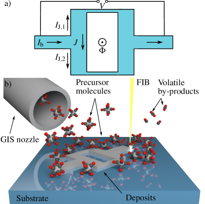
Direct current- (dc-) Superconducting Quantum Interference Devices (SQUIDs) are magnetic flux sensors that attain an unrivaled sensitivity [1, 2] by exploiting the physical effects of magnetic flux quantization [3] and Josephson effect [4]. A dc-SQUID consists of a superconducting ring interrupted by two Josephson junctions (JJs), one on either side (fig. 1). A JJ is formed by a superconductor (S) interrupted by either an insulator (I), a normal metal (N) or a weaker superconductor (s) resulting, respectively, in a SIS-, SNS- or SsS-junction that is capable of carrying a superconducting Josephson current, . The flux quantization within the superconducting ring is attained by the induction of a loop current, , which either opposes or supports the external magnetic field, lowering or rising the flux threading the ring to an integer multiple of the magnetic flux quantum, . The bias current, , injected into one of the arms of the SQUID splits into two phase-sensitive Josephson currents running simultaneously through both of the JJs and interfering in the second arm.
The sensitivity of SQUIDs is limited by the flux noise, , and the SQUID inductance, . The flux noise can be reduced by downsizing of the dimensions of the JJs [5], whereas the inductance can be reduced by decreasing the size of the effective inner SQUID area [6]. Ever since this revelation a lot of effort has been brought forth and various methods have been developed to fabricate nanoSQUIDs with ever lower geometrical dimensions and thus higher sensitivity [7, 8, 9].
While SQUIDs with SIS- or SNS-junctions commonly require a sandwich-type structure composed of multiple layers, SQUIDs based on SsS-junctions are planar and fabricated in a single layer. In this approach the JJs are realized by two constrictions in the SQUID loop, the Dayem Bridges (DBs) [10], forming regions with lower in the superconducting material. The low thickness of the planar DB-nanoSQUIDs makes them insusceptible to in-plane fields and enables for good coupling to magnetic nanoparticles. However, the dissipation of heat in the normal-conducting state of the DBs yields a hysteretic I-V characteristic in materials with high . Generally, the kinetic inductance, is high and can dominate the total inductance of the SQUID [1].
Conventionally, the design for a nanoSQUID is transferred to a resist by means of Electron Beam Lithography (EBL). The structure can either be deposited via evaporation of a superconducting material followed by lift-off or etched from a previously patterned superconducting film [11]. Processes based on EBL are well established and allow for complicated geometries with linewidths down to [5]. NanoSQUIDs based on DBs have been fabricated with an inner loop area of down to and a spin sensitivity of by means of EBL [11]. However, the resist-based EBL process requires multiple fabrication steps making it a time-consuming approach. A homogeneous film of the resist is obtained by spin-coating, requiring a large, flat substrate. Furthermore, the resulting structures are not perfectly symmetric and suffer from irregular edges [12].
Novel, sophisticated fabrication methods such as variable thickness DBs [13], superconducting \ceNb/\ceAl bilayers [14] and normal-conducting heat-sinks [9] could further increase the sensitivity, but also add to the complexity of the fabrication process. The currently smallest, most sensitive nanoSQUIDs are based on a complicated process of directional evaporation of a superconducting material onto a pulled quartz tube. Vasyukov et al. fabricated a circular SQUID with a diameter of , resulting in an inductance of and a spin sensitivity below making it capable of the detection of the spin of a single electron [15].
A different approach to creating superconducting devices using direct-write techniques is to start from a superconducting thin film and perform a FIB irradiation process to locally modify the electronic properties. This approach has allowed, for example, for the creation of high quality Josephson superconducting tunnelling junctions by irradiation with a focused \ceHe+ ion beam [16]. NanoSQUIDs with a DB-width of and a loop size of were fabricated by \ceGa+ FIB milling of a previously patterned \ceNb film in 1980 for the first time [5]. Recently, M. Wyss et al. used this technique to fabricate a SQUID on the tip of a capped AFM cantilever with a field sensitivity of [17]. However, the \ceNb in the DBs deteriorates due to the implantation of \ceGa and amorphization that occurs in the surface and up to below it.
An alternative to resist-based techniques or directional evaporation are direct-write techniques, such as Focused Electron / Ion Induced Deposition (FEBID / FIBID), which constitute versatile techniques for the fabrication of nanostructures on substrates of arbitrary size and topography [18, 19]. These techniques do not require the use of a resist and the entire nanostructure can be fabricated in a single step. Typically performed in either dedicated FIB instruments or in FIB/Scanning Electron Microscope (SEM) equipments, which host columns of both ions and electrons, the procedure begins by introducing a gaseous precursor containing the element of interest into the process chamber, which then adsorbs on the substrate. Upon local irradiation of the adsorbed molecules with the focused beam, the precursor is decomposed into a non-volatile constituent, which permanently remains deposited on the surface, and into volatile by-products that are pumped away by the vacuum system of the instrument. The resulting deposit is patterned following the shape of the scan traced by the beam (fig. 1). In the case of FIBID, concurrently with the deposition of the desired material, the FIB modifies the exposed material by ion implantation, amorphization and sputtering. In absence of a precursor gas these effects can be used to locally modify the physical properties of a given sample or to locally remove material by milling [20, 21].
The ability of FEBID/FIBID techniques to pattern very small features, together with their versatility for patterning on unconventional non-planar surfaces, and the well-established superconducting properties of \ceW-C or \ceNb-C based nanodeposits created either by FEBID [22] or FIBID [23], make these techniques very promising for the fabrication of nanoSQUIDs in a single writing step.
The superconducting properties of \ceW-C fabricated by \ceGa+ FIB irradiation of the commercially available precursor gas \ceW(CO)6 are well studied. Planar \ceGa+ FIBID \ceW-C deposits exhibit a critical temperature of [24, 25, 26, 27], an upper critical magnetic field of [28, 29, 30] and a critical current density of [25, 26, 27]. The London penetration depth is reported to be [31, 32] and the superconducting coherence length [31, 32, 33, 26]. Nanostructures with linewidths down to can be patterned with high precision and reproducibility [26].
Several remarkable applications for superconducting nanodevices fabricated by FIBID/FEBID have been reported thus far and are worth mentioning. \ceW-C deposits have been used to induce proximity superconducting effects on other materials [34] and to study the spin polarization of magnetic materials in Andreev contacts [35]. Besides, narrow W-C nanowires fabricated by \ceGa+ FIBID have been found to sustain long-range nonlocal flow of a single row of vortices, which could be of interest for manipulation of individual vortices in quantum technologies [36, 37], and allow tuning the value of the critical current by means of a gating voltage [32]. On the other hand, three-dimensional W-C nanostructures can be grown by \ceGa+ FIBID as freestanding pick-up loops coupled to a SQUID [38] and can be designed to support unconventional vortex patterns [39]. Recently, K. Lahabi and co-workers have characterized the electronic and magnetic-field dependent properties of JJs created by FEBID [22]. Superconducting properties of planar and 3D superconducting NWs based on \ceNb-C nanodeposits and fabricated by FEBID and \ceGa+ FIBID have also been studied [23, 40], with 3D nanowires exhibiting a higher critical temperature than their 2D counterparts.
The vast knowledge on the properties of \ceW-C and on how to tune them as desired, together with its commercial availability, make the \ceW(CO)6 precursor the perfect candidate for a broad range of approaches for the fabrication of nanoSQUIDs. In a single-step process a combination of normal- and superconducting materials can be used to fabricate SQUIDs based on both SNS- and SsS-JJs.
In this work, we present a method to nanofabricate \ceW-C based dc-SQUIDs with two DBs by means of focused \ceGa+ ion beam induced deposition on flat \ceSi/\ceSiO2 substrates. Section 2 describes the instruments and parameters used to carry out the experiments. Section 3.1 outlines the fabrication process that we have developed to fabricate nanoSQUIDs in a single writing step with high reproducibility and yield. In section 3.2 and section 3.3 the results of the characterization of the electric and magnetic properties of the dc-SQUIDs are outlined.
2 Experimental
The devices were grown on \ceSi substrates covered with a thermally-grown, thick \ceSiO2 surface layer. Prior to the deposition of the W-C nanoSQUIDs, a supporting Cr/Au structure, comprising the current and voltage leads for the electrical measurements of the devices, was patterned onto the substrates by optical lithography. A Süss MicroTec MA6 mask aligner, equipped with a mercury lamp, has been used to transfer the design to a thick \ceMMA resist layer. An electron beam deposition system (BOC EDWARDS Auto 500) has been used to metallize the sample with a \ceCr and a \ceAu layer followed by lift-off in acetone. The fine contacting structure was carried out via EBL in a ThermoFisher Scientific Helios NanoLab 600 FIB/SEM microscope controlled by a Raith ELPHY Plus pattern processor to a layer of \cePMMA resist. The metallization and lift-off steps were then repeated as described above.
The nanofabrication and imaging of the \ceW-C SQUIDs were performed in the same Helios 600 NanoLab FIB/SEM microscope, fitted with a \ceGa+ion column and a gas injection system (GIS) for precursor delivery. The imaging was performed with an electron beam current of at an acceleration voltage of . For the deposition of the \ceW-C material, an ion beam current of and an acceleration voltage of were used. The volume per dose was , the overlap was set to and the dwell time was . The base pressure of the FIB/SEM chamber was at , rising to during the injection of the \ceW(CO)6 precursor gas. The nozzle of the GIS was positioned at a vertical distance of and a in-plane displacement of from the irradiation point.
The low temperature characterization of the magnetotransport properties of the sample was performed in a commercial Quantum Design Physical Property Measurement System instrument. The base temperature for the characterization was . The samples were connected to the instrument via ultrasonic wire-bonding of \ceAl wires between the \ceCr/\ceAu leads and the instrument sample holder.
3 Results and discussion
3.1 Device fabrication
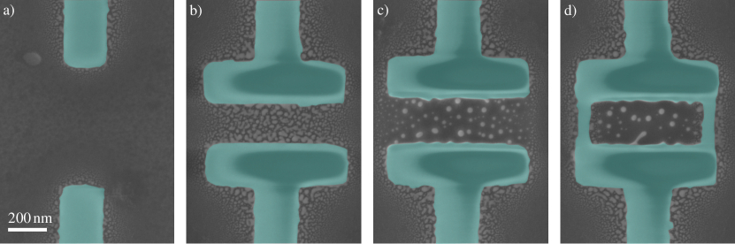
The fabrication of the nanodevices has been performed in a series of sequential steps (fig. 2), which include the fabrication of both the Josephson junctions and the main body of the nanoSQUID. In order to obtain the highest possible lateral resolution when depositing the nanowires, the lowest ion beam current of the FIB () was chosen. The current has been kept at this value for the whole structure.
After the process chamber was flushed with the precursor gas for , two -thick \ceW-C large leads were deposited to carry the injected current from the \ceAu leads to the device (fig. 2), taking . Thereafter, two rectangular pads with a thickness of were deposited in contact with the leads fabricated in the previous step, and positioned apart from each other (fig. 2), taking .
During the deposition of materials by FIBID, a common problem is the undesired deposition of material in the vicinity of the irradiated area, an issue commonly referred to as halo. In the case of conductive deposits, the halo can carry part of the injected current. This is the reason why the halo deposit must be eliminated to ensure proper device functionality. We observed a significant amount of halo in between the pads, i.e. at the effective loop area of the SQUID. Thus the fabrication was paused until the precursor gas was completely evacuated from the chamber, taking , and a short FIB milling step of of the effective loop area was performed (fig. 2) in order to remove the unwanted metallic deposits inside the inner loop area of the SQUID. Upon gas injection for , two nanowires acting as DBs were deposited connecting the two pads by their outer edges (fig. 2), taking . In total, the full fabrication process of the SQUID takes less than plus the time required to deposit the leads which strongly depends on their length. The nanowires have a cross-sectional area of . The overall nominal loop area of the SQUID is .
3.2 Superconducting properties
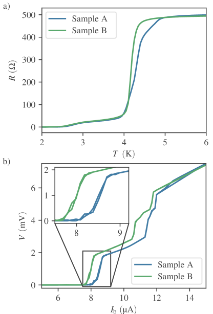
In this section we present the superconducting properties of two identically grown SQUIDs, labelled A and B, in absence of an external magnetic field. The samples were cooled down to the base temperature of while constantly injecting a bias current and measuring the resistance, . The temperature dependence of the resistance is shown in fig. 3. Both SQUIDs exhibit a transition to the superconducting regime at and , respectively. This is in good agreement with the results found in literature [33].
Thereafter, the current vs. voltage dependence was measured to obtain the critical current, shown in fig. 3. One can notice several transitions, attributed to, both the contact pads and the DBs. A quantitative analysis indicates that the critical current of the DBs equals and for sample A and B, respectively. Although DB-SQUIDs are expected to exhibit hysteretic behavior due to dissipation of heat in the normal conducting state of the constrictions [1] we do not observe a hysteresis in the I-V characteristics. We attribute the suppression of the hysteresis and the high transition width to an increase of the effective temperature in the noise parameter due to noise in the bias current [2]. The normal state resistance of the full structure, i.e. above all transitions, is and for each sample. Both the critical current and the critical temperature are very similar for the two nanoSQUIDs, confirming the reproducibility of the fabrication procedure. However, the transition width of sample B is smaller than that of sample A.
3.3 Magnetic response
In a JJ the macroscopic wavefunctions of the two separated superconductors overlap resulting in a phase-dependent Josephson current flowing through, given by
| (1) |
where denotes the maximal Josephson current and the phase difference between the two superconductors. In a dc-SQUID the flux quantization requires the phase of the two JJs to fulfill the condition
| (2) |
where the total flux is , being the inductance of the SQUID. The loop current ensures this condition by raising or lowering the total flux by . Assuming a negligible contribution of and we obtain the dependence of the critical current of the nanostructure on the external flux as
| (3) |
The quality of a SQUID can be characterized by the screening parameter
| (4) |
Equation 3 holds for with a critical current modulation . For a non-negligible influence of the critical current modulation decreases monotonically with an increasing screening parameter . This property allows one to estimate the inductance of the SQUID.
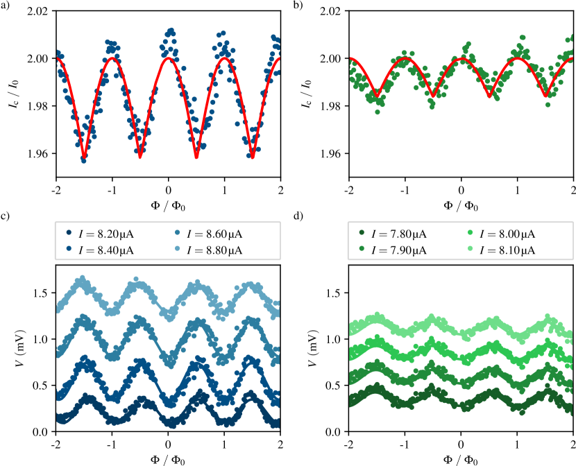
To extract we have measured several I-V characteristics of the SQUIDs at different values of perpendicularly-applied magnetic field. As the magnetic flux threading the SQUID loop is quantized in integer multiples of the magnetic flux quantum , it is possible to attribute each period of the oscillation in to a flux difference of . Figures 4 and 4 respectively show the dependence of the critical current of samples A and B (normalized to ) on the magnetic flux in units of . The red curve corresponds to the fit of the data to eq. 3 augmented by an offset current in order to account for the non-negligible :
| (5) |
The period of the oscillation in is similar in the two samples, with and . The effective areas deducted from this result are and . These are greater than the geometric loop area of which is to be expected due to the contribution of the kinetic inductance to the total inductance of the SQUID. Due to the high London penetration depth of \ceW-C and the low thickness of the SQUIDs, the screening of the magnetic field is comparably low, yielding a high kinetic inductance [1].
The amplitude of the oscillations yields the dimensionless screening parameter and , and the inductance of the devices, and . The magnetic properties of the two SQUIDs are comparable to one another. However, the determination of proved more error-prone due to the steeper transition in the I-V characteristics accounting for the minor differences between the samples.
Commonly, nanoSQUIDs are designed to have a screening parameter and are furthermore optimized to have a low inductance , which reduces the magnetic flux noise and thus improves the sensitivity to magnetic flux variations [1]. In DB-based SQUIDs based on \ceNb superconducting films ( [41]) inductance values in the regime are typically achieved [1].
The common operation mode of a dc-SQUID is its use as a flux-to-voltage transducer, where a constant bias current is injected and the voltage is measured, exhibiting a sinusoidal dependence on . In the vicinity of a linear dependence of on is obtained. The strongest variation of for a change of is characterized by the transfer coefficient
| (6) |
Thus, curves of constant have been extracted from the I-V characteristics. Figures 4 and 4 show curves for various values of of sample A and B, respectively. In sample A the transfer coefficient is for a bias current of . In sample B we obtain at . Typical values of the transfer function are in the range of [1]. The high transfer coefficient is attributed to the high normal state resistance of the \ceW-C nanoSQUIDs around , due to the high resistivity of this material [33] in comparison to other structures reported in the literature, which is commonly around [42, 43].
4 Outlook
This fabrication procedure serves as a proof of concept for the fabrication of \ceW-C nanoSQUIDs by means of \ceGa+ FIBID. It has the prospect to be modified and augmented in various ways. The conduction regime (normal- or superconducting) of the \ceW-C deposit can be controlled by deposition at various substrate temperatures (Cryo-FIBID) [44] or the use of an electron beam (FEBID) at different beam currents [22]. Thus the DBs can be readily replaced by a non-superconducting, FIBID-grown metal, resulting in SNS junctions. Thereby the fabrication of planar instead of sandwich-type SNS-JJ based nanoSQUIDs could be realized. A metallic heat-sink or a shunt resistor can be also added to the SQUID in a similar manner.
In recent years the development of SQUID on Tip (SOT) probes resulted in a new generation of Scanning SQUID Microscopes (SSMs) with unprecedented resolution and sensitivity for the mapping of the magnetic structure of a given surface [45, 46]. In this approach a SQUID is positioned on the tip of a pulled quartz tube via a three-step evaporation process. Lithographic methods require large, flat substrates and reach their limit with the high aspect ratio of the tip. The technique presented here poses a possible alternative approach for the fabrication of an SOT probe on commercially available Atomic Force Microscopy (AFM) cantilevers. The apex of the tip could be cut with the FIB and thereafter a SQUID could be deposited on the resulting flat area while maintaining the previously discussed flexibility in the SQUID design.
The comparably high inductance can be improved by both, a lower effective loop area and higher film thickness to enhance flux focusing. With \ceGa+ FIBID the feasible linewidth is at around and the London penetration depth is . Recent studies showed that both parameters could be improved by the use of \ceHe+ ions for the deposition of \ceW-C nanowires. Nanowires with a linewidth down to exhibit a London penetration depth of [47, 48, 36] making the material a promising candidate for the improvement of the process developed in this article. Further work towards the the optimization of the noise and sensitivity of the \ceW-C SQUIDs is underway.
5 Conclusion
In this work we have successfully fabricated two \ceW-C nanoSQUIDs with an inner loop area of in a fast \ceGa+ FIBID-FIB process (<). The SQUIDs exhibit a critical temperature of around and a critical current of around at . Albeit the London penetration length of \ceW-C is higher than that of similar devices of other materials, we have clearly observed oscillations of both the critical current and the voltage in dependence of the applied external magnetic field. The transfer coefficient is comparably high with up to , which we attribute to the high normal state resistance of the devices ().
The versatility of FIBID facilitates a high degree of freedom in the geometrical dimensions of the nanostructures and the substrate supporting the nanoSQUID, making the process a promising approach for the fabrication of SOT devices.
Author Contributions
F. S. performed the sample growth and the magnetotransport experiments, analyzed the data and wrote the first draft of the manuscript. P.O. contributed to the sample growth, data interpretation and the writing of the manuscript. S.S. and J.M.D.T. got the funding, supervised the research and contributed to the data interpretation and the writing of the manuscript.
Conflicts of interest
There are no conflicts to declare.
Acknowledgements
This research was supported by the European Commission under H2020 FET Open grant ‘FIBsuperProbes’ (number 892427), by the Spanish Ministry of Science through the grant PID2020-112914RB-I00, from CSIC through projects PIE202060E187 and Research Platform PTI-001, and by Gobierno de Aragón through the grant E13_20R with European Social Funds (Construyendo Europa desde Aragón). The following networking projects are acknowledged: Spanish Nanolito (RED2018-102627-T) and COST-FIT4NANO (action CA19140). Authors would like to acknowledge the use of Servicio General de Apoyo a la Investigación-SAI, Universidad de Zaragoza and the technical support provided by the LMA technicians at Universidad de Zaragoza. Furthermore we thank Julian Linek of the Physical Institute of the University of Tübingen (EKU) for the fruitful discussions.
References
- [1] Maria José Martínez-Pérez and Dieter Koelle “NanoSQUIDs: Basics & recent advances” In Physical Sciences Reviews 2.8, 2017, pp. 20175001 DOI: doi:10.1515/psr-2017-5001
- [2] Alex I. Braginski and John Clarke “The SQUID Handbook” John Wiley & Sons, Ltd, 2004, pp. 29–92 DOI: https://doi.org/10.1002/3527603646.ch1
- [3] F. London “Superfluids: Macroscopic theory of superconductivity”, Structure of matter series Wiley, 1950
- [4] B.D. Josephson “Possible new effects in superconductive tunnelling” In Physics Letters 1.7, 1962, pp. 251–253 DOI: https://doi.org/10.1016/0031-9163(62)91369-0
- [5] R.. Voss, R.. Laibowitz, M.. Ketchen and A.. Broers “Ultra low noise DC SQUIDS” Germany: de Gruyter, 1980
- [6] M.. Ketchen, T. Kopley and H. Ling “Miniature SQUID susceptometer” In Applied Physics Letters 44.10, 1984, pp. 1008–1010 DOI: 10.1063/1.94601
- [7] W. Wernsdorfer et al. “DC-SQUID magnetization measurements of single magnetic particles” In Journal of Magnetism and Magnetic Materials 145.1, 1995, pp. 33–39
- [8] John Gallop et al. “Miniature dc SQUID devices for the detection of single atomic spin-flips” In Physica C: Superconductivity 368.1, 2002, pp. 109–113
- [9] S… Lam and D.. Tilbrook “Development of a niobium nanosuperconducting quantum interference device for the detection of small spin populations” In Applied Physics Letters 82.7, 2003, pp. 1078–1080 DOI: 10.1063/1.1554770
- [10] P.. Anderson and A.. Dayem “Radio-Frequency Effects in Superconducting Thin Film Bridges” In Phys. Rev. Lett. 13 American Physical Society, 1964, pp. 195–197 DOI: 10.1103/PhysRevLett.13.195
- [11] W Wernsdorfer “From micro- to nano-SQUIDs: applications to nanomagnetism” In Superconductor Science and Technology 22.6 IOP Publishing, 2009, pp. 064013 DOI: 10.1088/0953-2048/22/6/064013
- [12] C P Foley and H Hilgenkamp “Why NanoSQUIDs are important: an introduction to the focus issue” In Superconductor Science and Technology 22.6 IOP Publishing, 2009, pp. 064001 DOI: 10.1088/0953-2048/22/6/064001
- [13] V. Bouchiat et al. “Josephson junctions and superconducting quantum interference devices made by local oxidation of niobium ultrathin films” In Applied Physics Letters 79.1, 2001, pp. 123–125 DOI: 10.1063/1.1382626
- [14] D. Hazra, J.. Kirtley and K. Hasselbach “Nano-superconducting quantum interference devices with suspended junctions” In Applied Physics Letters 104.15, 2014, pp. 152603 DOI: 10.1063/1.4871317
- [15] Denis Vasyukov et al. “A scanning superconducting quantum interference device with single electron spin sensitivity” In Nature Nanotechnology 8.9, 2013, pp. 639–644 DOI: 10.1038/nnano.2013.169
- [16] Shane A. Cybart et al. “Nano Josephson superconducting tunnel junctions in YBa2Cu3O7– directly patterned with a focused helium ion beam” In Nature Nanotechnology 10.7, 2015, pp. 598–602 DOI: 10.1038/nnano.2015.76
- [17] M. Wyss et al., 2021 arXiv:2109.06774 [cond-mat.mes-hall]
- [18] Ivo Utke, Patrik Hoffmann and John Melngailis “Gas-assisted focused electron beam and ion beam processing and fabrication” In Journal of Vacuum Science & Technology B: Microelectronics and Nanometer Structures Processing, Measurement, and Phenomena 26.4, 2008, pp. 1197–1276 DOI: 10.1116/1.2955728
- [19] Pablo Orús, Rosa Córdoba and José María De Teresa “Focused ion beam induced processing” In Nanofabrication, 2053-2563 IOP Publishing, 2020, pp. 1–28 DOI: 10.1088/978-0-7503-2608-7ch5
- [20] L.A. Giannuzzi and F.A. Stevie “A review of focused ion beam milling techniques for TEM specimen preparation” In Micron 30.3, 1999, pp. 197–204 DOI: https://doi.org/10.1016/S0968-4328(99)00005-0
- [21] D. Petit et al. “Nanometer scale patterning using focused ion beam milling” In Review of Scientific Instruments 76.2, 2005, pp. 026105 DOI: 10.1063/1.1844431
- [22] Tycho J. Blom et al. “Direct-Write Printing of Josephson Junctions in a Scanning Electron Microscope” In ACS Nano 15.1 American Chemical Society, 2021, pp. 322–329 DOI: 10.1021/acsnano.0c03656
- [23] Fabrizio Porrati et al. “Crystalline Niobium Carbide Superconducting Nanowires Prepared by Focused Ion Beam Direct Writing” In ACS Nano 13.6 American Chemical Society, 2019, pp. 6287–6296 DOI: 10.1021/acsnano.9b00059
- [24] E.S. Sadki, S. Ooi and K. Hirata “Focused ion beam induced deposition of superconducting thin films” In Physica C: Superconductivity and its Applications 426-431, 2005, pp. 1547–1551 DOI: https://doi.org/10.1016/j.physc.2005.02.151
- [25] I.. Luxmoore et al. “Low temperature electrical characterisation of tungsten nano-wires fabricated by electron and ion beam induced chemical vapour deposition” In Thin Solid Films 515.17, 2007, pp. 6791–6797 DOI: 10.1016/j.tsf.2007.02.029
- [26] R. Córdoba et al. “Magnetic field-induced dissipation-free state in superconducting nanostructures” In Nature Communications 4.1, 2013, pp. 1437 DOI: 10.1038/ncomms2437
- [27] D Spoddig et al. “Transport properties and growth parameters of PdC and WC nanowires prepared in a dual-beam microscope” In Nanotechnology 18.49 IOP Publishing, 2007, pp. 495202 DOI: 10.1088/0957-4484/18/49/495202
- [28] A. Helzel et al. “Nonlocal vortex motion in mesoscopic amorphous structures” In Phys. Rev. B 74 American Physical Society, 2006, pp. 220510 DOI: 10.1103/PhysRevB.74.220510
- [29] Jun Dai et al. “Superconductivity in Tungsten-Carbide Nanowires Deposited from the Mixtures of W(CO)6and C14H10” In Japanese Journal of Applied Physics 52.7R IOP Publishing, 2013, pp. 075001 DOI: 10.7567/jjap.52.075001
- [30] Yi Sun et al. “Voltage-current properties of superconducting amorphous tungsten nanostrips” In Scientific Reports 3.1, 2013, pp. 2307 DOI: 10.1038/srep02307
- [31] I. Guillamón et al. “Direct observation of melting in a two-dimensional superconducting vortex lattice” In Nature Physics 5.9, 2009, pp. 651–655 DOI: 10.1038/nphys1368
- [32] Pablo Orús, Vladimir M. Fomin, José María De Teresa and Rosa Córdoba “Critical current modulation induced by an electric field in superconducting tungsten-carbon nanowires” In Scientific Reports 11.1, 2021, pp. 17698 DOI: 10.1038/s41598-021-97075-z
- [33] E.. Sadki, S. Ooi and K. Hirata “Focused-ion-beam-induced deposition of superconducting nanowires” In Applied Physics Letters 85.25, 2004, pp. 6206–6208 DOI: 10.1063/1.1842367
- [34] Jian Wang et al. “Proximity-Induced Superconductivity in Nanowires: Minigap State and Differential Magnetoresistance Oscillations” In Phys. Rev. Lett. 102 American Physical Society, 2009, pp. 247003 DOI: 10.1103/PhysRevLett.102.247003
- [35] S. Sangiao, L. Morellón, M.R. Ibarra and J.M. De Teresa “Ferromagnet–superconductor nanocontacts grown by focused electron/ion beam techniques for current-in-plane Andreev Reflection measurements” In Solid State Communications 151.1, 2011, pp. 37–41 DOI: https://doi.org/10.1016/j.ssc.2010.10.028
- [36] Rosa Córdoba et al. “Long-range vortex transfer in superconducting nanowires” In Scientific Reports 9.1, 2019, pp. 12386 DOI: 10.1038/s41598-019-48887-7
- [37] T. Golod, A. Iovan and V.. Krasnov “Single Abrikosov vortices as quantized information bits” In Nature Communications 6.1, 2015, pp. 8628 DOI: 10.1038/ncomms9628
- [38] E.. Romans et al. “Three-dimensional nanoscale superconducting quantum interference device pickup loops” In Applied Physics Letters 97.22 American Institute of Physics, 2010, pp. 222506 DOI: 10.1063/1.3521262
- [39] Rosa Córdoba et al. “Three-Dimensional Superconducting Nanohelices Grown by He+-Focused-Ion-Beam Direct Writing” In Nano Letters 19.12 American Chemical Society, 2019, pp. 8597–8604 DOI: 10.1021/acs.nanolett.9b03153
- [40] O.. Dobrovolskiy et al. “Ultra-fast vortex motion in a direct-write Nb-C superconductor” In Nature Communications 11.1, 2020, pp. 3291 DOI: 10.1038/s41467-020-16987-y
- [41] B.. Maxfield and W.. McLean “Superconducting Penetration Depth of Niobium” In Phys. Rev. 139 American Physical Society, 1965, pp. A1515–A1522 DOI: 10.1103/PhysRev.139.A1515
- [42] Roberto Russo et al. “Performances of niobium planar nanointerferometers as a function of the temperature: a comparative study” In Superconductor Science and Technology 27.4 IOP Publishing, 2014, pp. 044028 DOI: 10.1088/0953-2048/27/4/044028
- [43] Aico G.. Troeman et al. “NanoSQUIDs Based on Niobium Constrictions” In Nano Letters 7.7 American Chemical Society, 2007, pp. 2152–2156 DOI: 10.1021/nl070870f
- [44] Rosa Córdoba et al. “Ultra-fast direct growth of metallic micro- and nano-structures by focused ion beam irradiation” In Scientific Reports 9.1, 2019, pp. 14076 DOI: 10.1038/s41598-019-50411-w
- [45] Amit Finkler et al. “Self-Aligned Nanoscale SQUID on a Tip” In Nano Letters 10.3 American Chemical Society, 2010, pp. 1046–1049 DOI: 10.1021/nl100009r
- [46] Y. Anahory et al. “SQUID-on-tip with single-electron spin sensitivity for high-field and ultra-low temperature nanomagnetic imaging” In Nanoscale 12 The Royal Society of Chemistry, 2020, pp. 3174–3182 DOI: 10.1039/C9NR08578E
- [47] J. Basset et al. “High kinetic inductance microwave resonators made by He-Beam assisted deposition of tungsten nanowires” In Applied Physics Letters 114.10 American Institute of Physics, 2019, pp. 102601 DOI: 10.1063/1.5080925
- [48] Pablo Orús, Rosa Córdoba, Gregor Hlawacek and José Marı́a De Teresa “Superconducting properties of in-plane W-C nanowires grown by He focused ion beam induced deposition” In Nanotechnology 32.8 IOP Publishing, 2020, pp. 085301 DOI: 10.1088/1361-6528/abc91c