Multi-Band Superconductivity in Strongly Hybridized 1T’-WTe2/NbSe2 Heterostructures
Abstract
The interplay of topology and superconductivity has become a subject of intense research in condensed matter physics for the pursuit of topologically non-trivial forms of superconducting pairing. An intrinsically normal-conducting material can inherit superconductivity via electrical contact to a parent superconductor via the proximity effect, usually understood as Andreev reflection at the interface between the distinct electronic structures of two separate conductors. However, at high interface transparency, strong coupling inevitably leads to changes in the band structure, locally, owing to hybridization of electronic states. Here, we investigate such strongly proximity-coupled heterostructures of monolayer 1T’-WTe2, grown on NbSe2 by van-der-Waals epitaxy. The superconducting local density of states (LDOS), resolved in scanning tunneling spectroscopy down to 500 mK, reflects a hybrid electronic structure, well-described by a multi-band framework based on the McMillan equations which captures the multi-band superconductivity inherent to the NbSe2 substrate and that induced by proximity in WTe2, self-consistently. Our material-specific tight-binding model captures the hybridized heterostructure quantitatively, and confirms that strong inter-layer hopping gives rise to a semi-metallic density of states in the 2D WTe2 bulk, even for nominally band-insulating crystals. The model further accurately predicts the measured order parameter meV induced in the WTe2 monolayer bulk, stable beyond a 2 T magnetic field. We believe that our detailed multi-band analysis of the hybrid electronic structure provides a useful tool for sensitive spatial mapping of induced order parameters in proximitized atomically thin topological materials.
I Introduction
Inducing superconductivity by proximity in materials with non-trivial band topology [1, 2, 3] has become a method of choice in the search for unconventional forms of superconducting pairing [4, 5]. Prominent examples are demonstrations of unconventional superconductivity in semiconductor nanowires with strong spin-orbit coupling [4], atomic chains and islands [5, 6], as well as at the surfaces and edges of three-dimensional topological insulators [7] and semimetals [8]. At the one-dimensional (1D) edges of 2D topological insulators [9, 10], such as the quantum spin Hall (QSH) state [11], the presence of non-Abelian parafermions have been predicted [12].
In any material system, topologically trivial or non-trivial, the proximity effect can be understood in a microscopic picture to result from Andreev reflection of quasiparticles at the superconductor / normal metal interface. The strength of the induced superconducting pairing is directly linked to the transparency of the interface, i.e. the tunneling coupling at the contact between the proximity-coupled materials. While strong induced pairing with a large order parameter may often be desired, e.g. to mitigate disorder or the effects of an applied magnetic field [4], it is often assumed that the tunnel-coupling does not induce any fundamental changes to the bandstructure. In stark contrast, exchange of charge, especially across atomically abrupt interfaces, can be expected to give rise to atomic-bonding or at least perturbations of the electronic structure, which can lead to profound changes in the electronic band dispersion [13].
Here, we investigate the hybrid electronic structure of such strongly-coupled heterostructures of the quantum spin Hall (QSH) candidate 1T’-WTe2, grown by in-situ van-der-Waals epitaxy on the type-II superconductor 2H-NbSe2. Scanning tunneling spectroscopy down to 500 mK allows us to resolve the superconducting local density of states (LDOS) which we analyze within a self-consistent multi-band framework based on the McMillan equations [14]. We are able to show that superconductivity is induced in a semi-metallic WTe2 monolayer bulk, which we understand as a result of a strong inter-layer tunneling across the heterointerface, leading hybridization of electronic states. A material-specific mean-field tight-binding model is able to capture the hybrid electronic structure in the normal state, allowing direct quantitative comparison with the measured LDOS. As a result, our model is able to predict the magnitude of the induced superconducting order parameter, quantitatively, robust to magnetic fields beyond 2 T. Owing to strong hybridization, we observe a significant weakening of the topological edge state signature, measurable by an enhancement of the LDOS in the normal state at the edge, concomitant with a slight enhancement of the induced superconducting order parameter.
Tungsten ditelluride (WTe2) and related members of the transition metal dichalcogenide family with 1T’ crystal structure have attracted much attention as candidates material system to realize type-II Weyl [15] fermions and higher-order topology [16] in its 3D bulk. Evidence of high-order semi-metallic properties have recently been confirmed in superconducting Josephson junction measurements [17, 18] showing that induced supercurrents are well-localized to the materials 1D edges (“hinges”). In atomic monolayers, a time-reversal symmetry protected 2D topologically insulating state [19] has been predicted, arising from inversion of the transition metal - and the chalcogen -orbitals, highly tunable by electric fields and strain [19]. While free-standing 1T’-WTe2 monolayers had initially been predicted to be semi-metallic with a negative fundamental band gap [19], a positive gap was later confirmed by density functional theory and layer-dependent optical spectroscopy [20]. Quantum spin Hall insulating behaviour and the presence of highly-confined 1D metallic states at the edge have since been confirmed in electron transport [21, 22], angle-resolved photoemission spectroscopy (ARPES), and scanning probe measurements [23, 24] including microwave impedance microscopy [25]. However, the sensitivity of the WTe2 band gap to strain [26] and electric fields [27] remains a matter of intense debate, as significant variations in the magnitude and definition of the measured QSH bulk are being observed [20, 21, 23, 22, 24, 28, 27]. Recent reports indicate that the bulk gap observed may indeed arise from 2D electronic interactions [28] challenging the band-insulating picture [29, 30].
The study of superconductivity remains of fundamental interest in both the QSH insulating [19, 31, 12] and semi-metallic [32, 33] states of 1T’-WTe2, given theoretical predictions of non-trivial pairing. Intrinsic low-density superconductivity has recently been reported in the 2D bulk of electrostatically doped semi-metallic WTe2 monolayers [34, 35], and is believed to be of non-trivial pairing [32, 33]. Similarly, the 1D helical edge of any quantum spin Hall insulating state has been predicted as a potential host for parafermions in the superconducting state [19, 10, 9, 31, 12].
Superconductivity up to relatively high critical temperatures and magnetic fields can be achieved by proximity-coupling to a stable intrinsic superconductor, such as the layered type-II superconductor 2H-NbSe2 ( K, T) [36, 37, 38, 39]. Further to these studies, here we show that strong coupling to the superconductor gives rise to a hybrid multi-band electronic structure, which needs to be taken into account when interpreting the detailed functional form of the induced superconducting local density of states.
II Results and Discussion
II.1 Crystal Growth and Atomic Structure
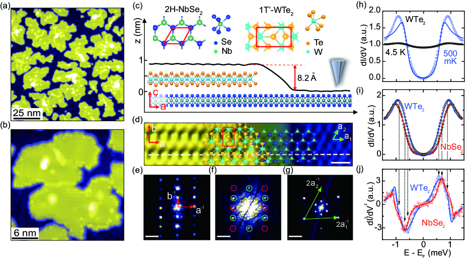
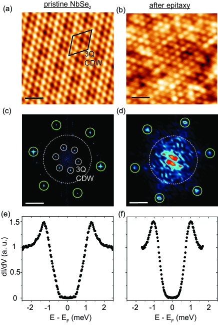
Figure 1 shows scanning tunneling microscopy (STM) data of 1T’-WTe2/2H-NbSe2 heterostructures, grown by bufferless low-temperature van-der-Waals epitaxy. In agreement with previous studies of WTe2 on bilayer graphene (BLG) [23, 24], we observe Volmer-Weber growth of islands with disordered boundaries (Figs. 1(a) and 1(b)) and size up to a few tens of nanometre in diameter, that are poly-crystalline on NbSe2 substrates. For this work, we focus on the intermediate coverage limit (%) in order to maximize the density of QSH edges, although nearly complete monolayers with coverage of 95% can be achieved with reduced crystal quality.
Atomic-level detail of the WTe2 lattice alignment with the substrate is shown in Figs. 1(d)-1(g) where we find that the respective chalcogen (Te and Se) sublattices align along the atomic rows of 1T’-WTe2 (-direction). A 2D fast Fourier transform (Fig. 1(f)) of an area with % WTe2 monolayer coverage indeed confirms that the Bragg peaks of the WTe2 and NbSe2 lattices coincide within the accuracy of the measurement. We extract Å, and Å , in good agreement with the lattice parameters of WTe2 ( Å, and Å ) [20]. Åare the lattice parameters of NbSe2, local lattice matching would imply a 5% compressive lattice strain along , which has previously been shown to further stabilize the WTe2 bulk gap [26].
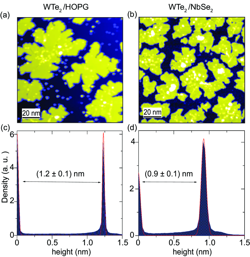
A first indication that we may expect strong hybridization in WTe2/NbSe2 heterostructures comes from a measurement of the monolayer height nm, extracted from -height distributions of large-scale topographic STM images (see Fig. 5, Appendix A), and is comparable to measurements of van-der-Waals stacked WTe2/NbSe2 ( nm) [39]. The significantly lower layer height, compared to WTe2/BLG ( nm) [24] and WTe2/HOPG ( nm) (this work), suggests a smaller van-der-Waals gap, resulting in stronger interlayer coupling and hybridization of electronic states.
We observe some variations in the electronic structure across different monolayer crystals, reflecting varying doping levels and the presence of in-gap impurity states around the visible adatom disorder (Figs. 1(a)-(b). We therefore focus on spectra obtained on clean monolayer regions which display a clear suppression of the LDOS over an energy range of several tens of meV around the Fermi energy, and with signatures of an edge state in the normal state. As shown in the comparison of Fig. 2 below, such spectra agree well with tight-binding calculations of the normal state electronic structure, as well as with those published on WTe2/BLG [23, 24, 26, 27]. Given the metallic nature of the two substrates used in this work, we do not expect that exitonic insulating effects [29, 30] play a dominant role here, as Coulomb interaction would be expected to be strongly screened.
II.2 Multi-Band Superconductivity
The clear signature of a superconducting energy gap, measured in the 2D bulk of monolayer WTe2, is shown in Figs. 1(h), comparing the superconducting LDOS at 4.5 K with that measured at 500 mK. Fits to conventional BCS theory (solid lines) describe the data well only at 4.5 K, but fail to describe the details of the energy gap resolved at 500 mK. This becomes particularly apparent by an underestimation of the width and height of the coherence peaks at meV. A comparison of high-resolution spectra measured, respectively, on the WTe2 and NbSe2 surfaces, are shown in Fig. 1(i). We observe a slightly reduced gap size on NbSe2 post MBE growth, compared to the pristine NbSe2 surface, which is likely due to a partial quenching of the 3Q charge density wave (CDW) order [40, 41] leading to disorder averaging of the Fermi surface anisotropy and reduced inter-band coupling (see Fig. 7 and Appendix B for further detail). A further reduction of the superconducting gap measured on WTe2/NbSe2 corroborates that superconductivity is induced into the monolayer via the substrate.
As detailed below, we are able to accurately describe the measured superconducting LDOS within a self-consistent multi-band framework based on the McMillan equations [14, 42, 41] (blue/red lines). In the presence of multiple non-interacting bands , the superconducting density of states can be expressed as a simple sum of two or more partial densities of states,
| (1) |
Within conventional BCS theory, the order parameter is a constant and the prefactor. The prefactor, ), denotes the partial state density of states of band in the normal state and, in the superconducting state, takes the role [41] of an effective partial density of states weight to the total density of states (Eq. (6)). An additional broadening parameter is usually included to account for energy broadening during the tunneling process (Dynes parameter) [43].
Different from BCS theory, the McMillan model [14] considers coupled bands with order parameters , that are energy-dependent complex functions of the form
| (2) |
Here, an inter-band Cooper pair tunneling across the van-der-Waals gap at rate renormalizes the intrinsic order parameters of the separate materials , leading to a set of self-consistent equations, that can be solved numerically to fit our data.
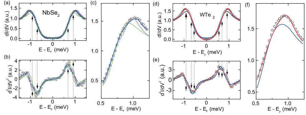
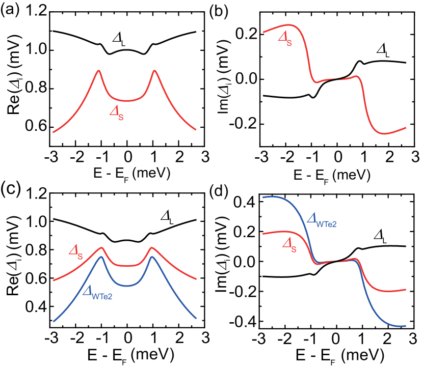
Although originally developed to describe the superconducting proximity effect in single-band metallic systems, the McMillan model has more recently been successfully applied to describe intrinsic multi-band superconductivity in layered two-band superconductors [42], including NbSe2 [41, 44]. For this work, we further extend the McMillan model to describe the hybrid electronic structure of 1T’-WTe2/NbSe2 heterostructures, thus treating multi-band superconductivity and proximity-coupling within the same theoretical framework. To this end, we consider a third order parameter , coupled to the NbSe2 -band (see supporting information), assuming . Fits to both a two-band (NbSe2, red line) and a three-band (WTe2/NbSe2, blue line) model describe the data well (Fig. 1(i)), and reproduce the known NbSe2 order parameters (see Table 1. Indeed, we find that simpler BCS-based models are unable to represent the data well at 500 mK (Appendix B), further confirming the multi-band hybrid electronic structure. For the real part of the induced order parameter, we find meV, reflecting induced pairing in the strongly coupled heterostructure, in reasonable agreement with recent transport [38] and local probe [39] spectroscopy of non-epitaxial WTe2/NbSe2 hetero-junctions.
II.3 Hybrid Electronic Structure
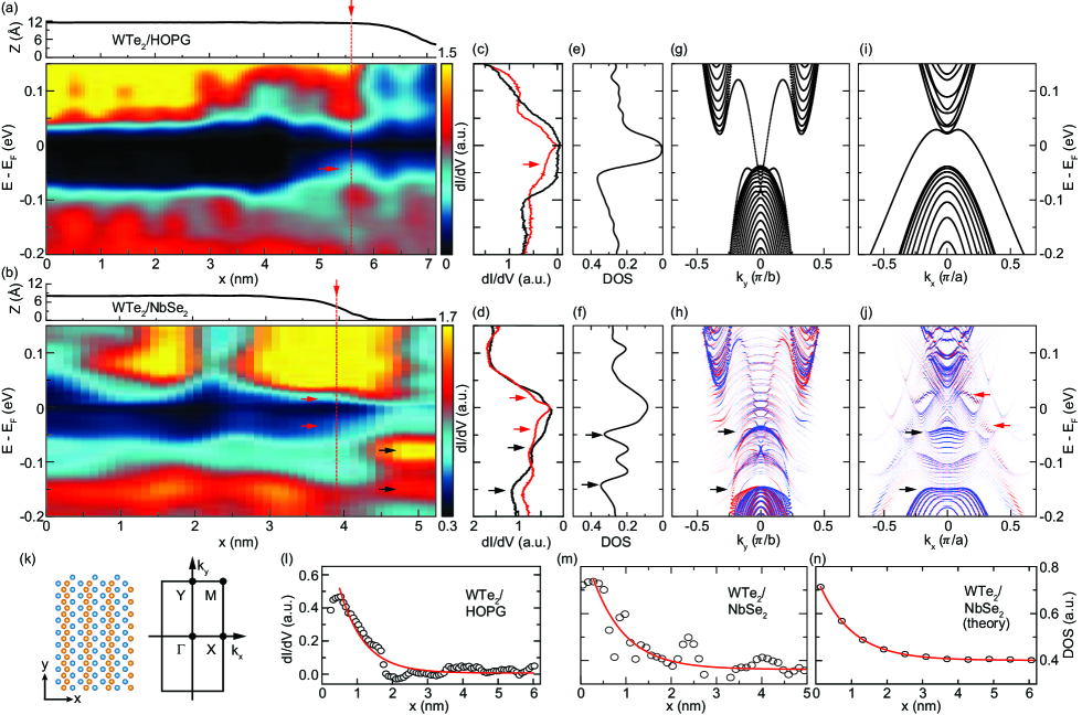
As inferred from our three-band model, we understand that superconductivity is induced in the WTe2 bulk as a result of strong inter-band coupling to the substrate giving rise to a WTe2/NbSe2 hybrid electronic structure. We confirm this notion in Fig. 2 by directly comparing spectra of the normal-state LDOS with tight-binding band structure calculations [45] (Appendix F). In Figs. 2(a) and 2(b) we show the spatial evolution of the measured normal-state LDOS across a monolayer edge, comparing the WTe2/HOPG (a) and the WTe2/NbSe2 (b) heterostructure, alongside corresponding height-profiles. Individual point spectra of the 2D bulk (black) and 1D edge (red) are furthermore shown in the inserts to Figs. 2(c) and (d). In both heterostructures, the LDOS shows clear signs of a suppression over meV around the Fermi energy, corresponding to a soft gap. This gap is significantly more developed in WTe2/HOPG, but shows with comparable magnitude and position also on WTe2/NbSe2. A residual 2D bulk LDOS within the gap is measurable on both substrates, but is much more pronounced in WTe2/NbSe2, attesting to strong hybridization in the heterostructure.
Tight-binding band structure calculations of a freestanding WTe2 monolayer are shown in Fig. 2(c), and compared with the spin-resolved WTe2 orbital weight of the hybridized WTe2/NbSe2 heterostructure (Fig. 2(d). We find best agreement for an interlayer hopping of 0.15 eV (see Appendix), similar in magnitude to the Nb-Nb hopping strength within the 2H-NbSe2 cell [46]. A slightly larger hopping strength would be expected given the shorter Nb-Te separation. The direct comparison with our measured spectra (inserts) shows reasonable agreement with regard to the position of the band edges (horizontal dashed lines), the Fermi energy (), as well as edge state features (red arrows). Indeed, the WTe2/HOPG spectra resemble closely those previously reported for monolayer WTe2 grown on bilayer graphene, [23, 24] indicating that heterostructures with graphitic substrates are only weakly hybridized. The additional spectral features (black arrows), however, only observed in the WTe2/NbSe2 heterostructure, need to be attributed the presence of a NbSe2 partial DOS (reference spectrum in the left-hand insert to Fig. 2(d)), confirming the hybridization picture.
As a result of the strong hybridization in WTe2/NbSe2, we further observe a substantial weakening of the topological edge state signature, compared to our observations on WTe2/HOPG and WTe2/BLG[23, 24, 26, 27]. This is illustrated in Figs. 2(e)-2(g) by plotting spatial profiles of the integrated LDOS within the gap (-50 meV and +20 meV) away from the edge position. We extract roughly consistent exponential decay lengths of nm for both heterostructures. However, the ratio of the edge state LDOS to that in the bulk is much lower for WTe2/NbSe2 (), compared to WTe2/HOPG (), given the large residual LDOS in the bulk gap. Both edge state decay length and LDOS ratio agree well with our tight-binding calculations of the hybrid electronic structure for WTe2/NbSe2 as shown in Fig. 2(g).
In Fig. 3, we plot the calculated superconducting LDOS for the same inter-layer hopping (0.15 eV) as used for both the band structure calculation in Fig. 2(d) and the LDOS profile in Fig. 2(g). We extract meV on the top-most tellurium sublattice, which the STM is expected to be most sensitive to, in remarkable agreement with the experiment ( meV), as extracted from our three-band fits.
The magnetic field stability of superconducting pairing in the WTe2 monolayer bulk is investigated in Fig. 3(b), where we plot the measured superconducting LDOS for magnetic fields up to T, applied perpendicular to the sample plane (-axis).

II.4 Spatial Profile at the Monolayer Edge
In Fig. 4, we investigate the spatial evolution of the superconducting LDOS across the WTe2 monolayer edge. An atomic resolution STM image of a clean WTe2 edge is shown in Fig. 4(a), indicating position and direction of the STM height profile. The spatial dependence of the superconducting energy gap, measured at 500 mK, is shown Fig. 4(b), alongside the superconducting partial density of states weight of the WTe2/NbSe2 heterostructure (Fig. 4(c)). The latter has been extracted self-consistently, using Eqns. (1) and (9). We observe a pronounced crossover in the partial density of states at ( nm), coinciding with the edge position, beyond which the WTe2 DOS drops to zero as the STM tip leaves the monolayer crystal. In the monolayer bulk, we find that WTe2 dominates the total DOS with %, with a contribution of % by the NbSe2 substrate partial DOS. Interestingly, a more pronounced enhancement in the superconducting partial DOS at the edge appears absent, at least when compared to the normal-state DOS in Fig. 2(f). This is likely due to the vanishing total LDOS at the edge at seen in the normal state (compare red curves in Figs. 2(c) and 2(d), possibly due to the presence of an interaction driven pseudogap [47, 48, 23, 49].
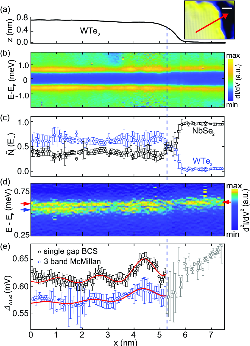
A further confirmation of three-band superconductivity is given in Fig. 4(d) where we plot the spatial profile of the second derivative of the tunneling current for energies close to the coherence peak. We observe a sharp transition from two-band to three-band signatures as soon as the probe tip crosses the monolayer edge (dashed line). Arrows indicate the gap energies for the WTe2 induced gap (blue) and the intrinsic NbSe2 small gap (red). The NbSe2 large gap at higher energy is not seen here, but is indicated in Figs. 8(a) and 8(b) of the Appendix.
A spatial profile of the extracted order parameter is shown in Fig. 4(e), in which we observe spatial oscillations with a period of nm. Oscillations of comparable period are also observed in the order parameter extracted from a simple single-band BCS model, as well as are visible in the energy-integrated normal-state LDOS (Fig. 2(f)). This suggests that these arise from Friedel-like oscillations in the local density of states due to scattering of 2D bulk states at the WTe2 edge. Indeed, we can fit the extracted order parameter with a simple empirical model,
| (3) |
in which the first term reflects the oscillatory behaviour in the local order parameter due to quasiparticle-interference in the 2D bulk. The second term accounts for a residual enhancement of the exponentially decaying 1D edge state, with decay length nm comparable to our measurements of the normal state LDOS (Fig. 2(g)). The simple model thus simultaneously confirms the edge position ( nm) and the Fermi wave vector[50] nm-1, and the edge state decay length. Upon crossing the edge, increases to approach the smaller of the two renormalized order parameters of NbSe2 ( meV) as the three-band model emulates the two-band superconductivity of the substrate. This transition coincides with a vanishing WTe2 partial DOS, which confirms that the greyed-out data points in Fig. 4(e) do not contribute any significant spectral weight to the overall measured density of states.
III Conclusions
In summary, we have reported signatures of multi-band superconductivity in strongly-coupled 1T’-WTe2/NbSe2 heterostructures, grown by van-der-Waals epitaxy. Analyzing the superconducting density of states down to 500 mK in scanning probe spectroscopy, we have shown that strong hybridization of electronic states gives rise to a semimetallic density of states in the 2D bulk even in nominally band-insulating crystals. Describing the detailed functional form of the superconducting energy gap in a self-consistent multi-band framework, based on the McMillan equations, we confirm the strong inter-band coupling. Our quantitative comparison of the measured local density of states with a material-specific tight-binding model ultimately confirms the hybrid electronic structure, in both normal and superconducting states for the same interlayer hopping, thus accurately predicting the magnitude of the induced WTe2 order parameter, meV, stable beyond a 2 T magnetic field. Despite the strong hybridization, we find that a measurable enhancement of the measured local density of states persists at the crystal edges, detectable in both the normal state and in a slight enhancement of the order parameter in the superconducting state. We believe that our multi-band treatment of strongly hybridized van-der-Waals heterostructures will form a useful tool to mapping spatial variation of the induced superconducting order parameter in wider range proximitized atomically-thin topological materials [51].
Acknowledgements
This research is supported by National Research Foundation (NRF) Singapore, under the Competitive Research Programme ”Towards On-Chip Topological Quantum Devices” (NRF-CRP21-2018-0001), with partial support from a Singapore Ministry of Education (MOE) Academic Research Fund Tier 3 grant (MOE2018-T3-1-002). The work was supported in part by Grants-in-Aid for Scientific Research from the Japan Society for the Promotion of Science (nos. 16H02109, 18K19013, and 19H00859). The work at Northeastern University was supported by the US Department of Energy (DOE), Office of Science, Basic Energy Sciences grant number DE-SC0019275 and benefited from Northeastern University’s Advanced Scientific Computation Center (ASCC) and the NERSC supercomputing center through DOE grant number DE-AC02-05CH11231. KEJG acknowledges support from the Agency for Science, Technology and Research (A*STAR) under its A*STAR QTE Grant No. A1685b0005. H.L. acknowledges the support by the Ministry of Science and Technology (MOST) in Taiwan under grant number MOST 109-2112-M-001-014-MY3. SM would like to acknowledge the new faculty seed grant from IIT Madras under project number Project No: PHY/18-19/703/NFSC/SHAA. BW acknowledges a Singapore National Research Foundation (NRF) Fellowship (NRF-NRFF2017-11). We thank Jack T. Hellerstedt for technical advice during the early stages of crystal growth.
Appendix A: 1T’-WTe2 Crystal Growth
Van-der-Waals molecular beam epitaxy (MBE) was performed in an Omicron Lab10 MBE (base pressure mBar) on bulk crystals of 2H-NbSe2 (HQ graphene, Netherlands) and highly oriented pyrolytic graphite (HOPG). The substrates were mechanically cleaved in UHV after degassing overnight (300° C), following co-deposition of W (99.998) and Te (99.999) for approximately 1h at a Te:W flux ratio of roughly 260:1. We use slightly different substrate temperatures for the two heterostructures with 145° C for 1T’-WTe2/NbSe2, and 230° C for 1T’-WTe2/HOPG. Typical STM images of the WTe2/HOPG and WTe2/NbSe2 heterostructures, respectively, are shown in Fig. 5(a) and 5(b), alongisde measurements of the respective WTe2 monolayer height, extracted from -height histograms 5(c) and 5(d).
Appendix B: Electronic Structure and Superconductivity of NbSe2
NbSe2 is a type-II superconductor [52, 53] with a critical temperature K and field T [54, 55]. The microscopic detail of its superconductivity have been investigated, intensively, both theoretically and experimentally [40, 41, 36, 56].
| Model | Measured Gap (meV) | Reference | Experiment |
|---|---|---|---|
| [39] | STS | ||
| Two-band (BCS) | [38] | Specific Heat | |
| [57] | Specific Heat | ||
| [57] | Specific Heat | ||
| Single-band (anisotropic) | [58] | Penetration length | |
| [56] | Electron transport | ||
| [41] | STS | ||
| Two-band McMillan | [44] | Electron transport | |
| this work | STS |
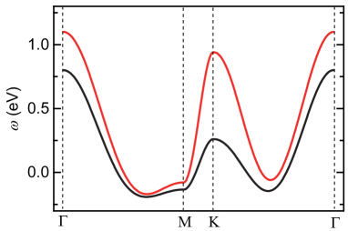
The NbSe2 Fermi surface [59, 46, 60] is composed of at least two bands at the Fermi energy. Tight-binding calculations of the NbSe22 low-energy bandstructure are shown in Fig. 6, where black and red lines are bands due to the orbitals, centered on the two Nb atoms within the unit cell (Nb bands). These form bonding and anti-bonding orbitals, giving rise to cylinders at the six -points of the hexagonal Brillouin zone. A third band (predominantly Se) [40] has been neglected in our model, as it is not believed to contribute to multi-band superconductivity in NbSe2 [40]. As a result of the two-band nature, two distinct superconducting energy gaps, and , are usually observed at very low temperatures () [41, 38, 57] (see Table 1), each hosted within the two Nb bands [40, 41, 44]. Superconducting pairing is significantly stronger in the Nb -bands [40, 41, 36], giving rise to the larger of the two gaps meV. At , the pairing is weaker with order parameter , and is usually found ranging between meV [41, 36].
CDW order on the pristine NbSe2 surface also plays an important role in scanning tunneling microscopy measurements of the superconducting gap. In pristine NbSe2, the 3Q charge density wave (CDW) gives rise to an anisotropic Fermi surface and a reduced Brillouin zone with hexagonal symmetry [41]. Possible mechanism for a suppression of have been argued to result from a reduction of the highly anisotropic superconducting gap due to disorder averaging and/or from the suppression of assistive short range CDW correlations [61]. From a multi-band perspective, the CDW wave vectors link states at the point (associated with the NbSe2 small gap) to the Nb cylinders at (associated with the large gap). This allows for the observation of the large gap on pristine NbSe2 surfaces in scanning tunnelling experiments [40, 41], which are most sensitive to states at (tunnelling of electrons with finite transverse momentum is strongly suppressed in STM due to the vertical tunneling path). Once CDW order is suppressed, STM will predominantly probe states at , which would explain the reduced gap observed [41]. Figure 7 shows a comparison of the measured gap on both the pristine and the post-growth NbSe2 surface, with a reduction in gap size clearly visible.
Appendix C: Comparison of Different Models for the Superconducting Density of States
Low-temperature scanning tunneling spectroscopy (STM/STS) measurements were carried out in an Omicron low-temperature STM (junction temperature K) and a Unisoku USM1300 He-3 STM (junction temperature mK), respectively. Spectroscopic measurements were obtained using standard lock-in techniques, with an AC excitation of amplitude of 1.5 mV at 831 Hz for measurements of the normal-state electronic structure, and V at 931 Hz for measurements in the superconducting state. In all measurements, we fix the current set point 200 pA at 10 mV, ahead of spectroscopy. All spectra of superconducting states through the paper have been spatially averaged, symmetrised about zero bias, and normalised with respect to the normal state conductance, unless otherwise specified.
In the limit of low bias and low temperature (), the tunneling differential conductance, measured by scanning probe spectroscopy, is usually expressed as a convolution of the tunneling density of states and the derivative of the Fermi-Dirac distribution,
| (4) |
For a bulk superconductor with a single isotropic band, a Bardeen-Cooper-Schrieffer (BCS) density of states is often assumed, and can result in acceptable fits at moderate temperature . However, as the derivative of the Fermi-Dirac distribution is a peaked function with half-width , it is responsible for thermal smearing of the measured superconducting tunneling density of states. An additional phenomenological broadening parameter, (Dynes parameter [43]) is often considered for tunneling experiments, accounting for additional pair-breaking mechanisms.
| (5) |
At low temperature (), fine detail of the functional form of the superconducting energy gap can be observed [40, 44, 56]. Indeed, in Fig. 1(h) we see that a BCS/Dynes model provides a good fit only at K, but fails to describe the detail of the measured superconducting density of states at lower temperature. A more detailed model is needed to describe the low-temperature data, taking the multi-band nature of superconductivity in NbSe2 into account.
In the presence of multiple (non-interacting) bands at the Fermi energy, the total tunneling density of states may be expressed as a sum over two or more partial densities of states,
| (6) |
The partial densities of states can further be expressed as
| (7) |
where it is assumed that the order parameter may not be constant, but itself be a complex energy-dependent and (potentially anisotropic [56]) function. The prefactor, , can be interpreted [41] as an effective partial density of states weight, renormalized from the true density of states by the tunneling probability into band .
Figure 8 shows a comparison of different models to fit our data, based on Eq. (1), including a single-band BCS/Dynes model (), a two-band BCS/Dynes model (), and an anisotropic single-band model (). The second derivative of the tunneling current and close-ups of the coherence peaks are shown alongside to clarify differences in the models. For the anisotropic model we have assumed an empirical anisotropy function, as previously employed for NbSe2 [56], reflecting the sixfold symmetry of the NbSe2 Fermi surface,
| (8) |
Appendix D: The McMillan Model
| Band | Model | (meV) | (meV) | |||
|---|---|---|---|---|---|---|
| 3 band | ||||||
| (Nb -point) | 2 band | |||||
| =S | 3 band | |||||
| (Nb -point) | 2 band | |||||
| =3 | 3 band | 0 | ||||
| (WTe2) | 2 band |
Taking the multi-band nature of superconductivity in NbSe2 into account, a compelling model to describe the superconducting density of states was employed by Noat et al. [41], based on the McMillan equations [14]. The McMillan model was originally developed to describe superconductivity between two proximity-coupled materials , in which the intrinsic order parameters are renormalised by an inter-layer electronic coupling of strength . In the context of multi-band superconductivity [42, 40, 41] the inter-layer coupling has since been interpreted as an inter-band scattering rate from band to band (“proximity-effect in reciprocal space”). Different from the other models discussed above, the order parameter in the McMillan model is a complex, energy-dependent gap function
| (9) |
Inclusion of these order parameters in Eq. (1) gives rise to a set of self-consistent equations to describe the multi-band system, that can be solved numerically to fit the measured tunneling spectra.
As highlighted in Ref. [41], in addition to the directly measured partial density of states (Eq. (1)), and independent estimate of the partial densities of states ratio at the Fermi-energy can be obtained from a ratio of the inter-band coupling parameters. Simultaneous extraction of both during the self-consistent numerical fits thus allow for an accurate extraction.
To describe multi-band superconductivity in the hybrid WTe2/NbSe2 heterostructure, we consider a third order parameter, , in Eq. 1. To limit the number of free parameters, we consider coupling only between WTe2 and the Nb -band (large gap ), which is expected to have the strongest contribution to the proximity coupling [41], and fix . We further assume that WTe2 does not carry any intrinsic superconductivity, such that . Finally, all NbSe2 related parameters – determined independently from two-band fits to the substrate – can be fixed in the three-band model, in particular, and , leaving only three independent fitting parameters in the three-band model.
Figures 8(d)-8(f) shows a comparison our three band McMillan model (solid red line) and the previous two-band model (solid blue line), applied to the WTe2/NbSe2 heterostructure. Importantly, a two-band model cannot represent the data well. From the three band model of the heterostructure, we are able to extract the intrinsic NbSe2 order parameters meV and meV, in excellent agreement those extracted from the two-band model of NbSe2 [44, 41]. Consistency of the NbSe2 order parameter, extracted separately from two-band and three band models, confirm that the properties of the NbSe2 parent superconductor remain unaffected by the presence of the WTe2 epilayer. The renormalised complex order parameters extracted from the three-band fits are plotted in Figs. 9(c) and 9(d). Here, we observe only a minor re-balancing of the inter-band tunneling rates with a concomitant small decrease in the Re(), as a result of the additional coupling to the third band. The value of the induced order parameter, meV agrees well with recent local probe [39] and transport spectroscopy [38] of non-epitaxial heterostructures.
Appendix F: Mean Field Theoretical Modelling of the Hybrid Bandstructure
The 1T’-WTe2/2H-NbSe2 heterostructure was modelled using a real-space mean field tight-binding Hamiltonian that is solved using a Bogoliubov-De-Gennes (BdG) formalism. The Hamiltonian contains four separate parts given by,
| (10) |
The individual terms of the Hamiltonian are given by,
In operators represent the creation and annihilation operators, respectively, at the site with a single Nb orbital contributing per site (see below for details). The layer index corresponds to the two layers of 2H-NbSe2, respectively, taking spin into account. The individual real-space tight-binding hopping matrix elements for 2H-NbSe2 are generated by a basis transformation to orbital basis from a two-band Hamiltonian that has been studied previously to match ARPES [62] and STM experiments [63] on 2H-NbSe2.
At temperatures below K, pristine NbSe2 undergoes a transition to a superconducting state. Assuming a dominant conventional -wave superconducting instability, we calculate the superconducting gap self-consistently at each lattice site by solving the BdG equations. The dominant on-site pairing term is tuned to generate a superconducting gap of eV in agreement with the experimental results on pristine 2H-NbSe2 (see Table 1 and references therein).
The electronic structure of 1T’-WTe2 is modelled by generating a real space version of an 8-band Hamiltonian, containing 2 Te and 2 W atoms in a rectangular unit cell. As discussed in Ref [45, 64, 65], this Hamiltonian corresponds to a dominant contribution from Te orbitals, and W orbitals, which dominate the low-energy band structure owing to the distorted lattice structure in monolayer 1T’-WTe2.
In , the indices refer to the unit cell, and represent the atoms or orbitals within each unit cell. The model provides reasonable agreement with the low energy electronic structure including the QSHI observed in ARPES and STM experiments [23]. In the enclosed additional supplementary files, we provide the real space hopping matrix elements including the Rashba spin orbit coupling terms included in the real space Hamiltonian for 1T’-WTe2. The monolayer edge was modelled using an open boundary condition and has been studied for various terminations for directions perpendicular and parallel to the direction of the atomic chains. We find that although the modelling of the edge with open boundary conditions is simplistic (the edge in as as-grown real material is rough with no consistent termination), the obtained local density of states shows reasonable agreement with the experiments (see Fig. 2 of the main text).
To represent a finite electronic interlayer coupling in the heterostructure, we assume a nearest neighbor hopping , leading to an effective hybridization between the Nb d orbitals and Te px orbitals. This gives rise to a residual metallic density of states within the WTe2 bulk band gap, in reasonable agreement with our experimental observations in both the normal state (see Fig. 2 of the main text) and the superconducting state (see Fig. 3 of the main text). We find best agreement with the experiments – simultaneously for normal and superconducting state – for eV.
The induced superconducting gap on the Te and W atoms have been evaluated self consistently by calculating the anomalous averages , where represents the 2 Te and 2 W atoms in the unit cell and is the unit cell index. The calculations involve a Hamiltonian where the electron operators are considered in momentum space for a direction perpendicular to the edge. For an edge along the -direction, the Bogoliubov-de-Gennes transformations involve quasi-article operators,
| (11) | |||||
| (12) |
Here, are the quasiparticle operators corresponding to state and are the corresponding amplitudes. Similar transformations also hold for the operators for NbSe2.
Diagonalizing the above BdG Hamiltonian, we self-consistently calculate the electron density and superconducting gap at each lattice site for the multi-orbital Hamiltonian. The mean-fields for the electron density would in general be given by,
| (13) |
Here, is the Fermi function.
As discussed above, the superconducting gap on NbSe2 has been introduced with a pairing interaction term . The self-consistent procedure leads to an induced even parity () order parameter on 1T’-WTe2. The induced superconducting gaps are obtained from the self-consistent solutions by calculating the following anomalous averages,
Here, is the number of divisions which is typically taken to be points to achieve high resolution for the small gaps observed in the system.
We see our model as a generalization from the approximation of a superconducting heterostructure by considering pristine WTe2 with no effect of the proximal superconductor on the WTe2 band structure, i.e. a heterostructure in which the only effect of the superconductor is to induce a gap on the QSH edges. Instead, our modelling accounts for a realistic finite interlayer coupling between NbSe2 and WTe2 through a self-consistent procedure, allowing for minor changes in the electronic structure such as hybridization and charge transfer. Our model is thus able to explain, simultaneously, a small but finite metallic density of states within the QSH gap, that leaves the edge state intact, and an induced superconducting order parameter of the same magnitude as resolved in the experiments.
References
- Fu and Kane [2008] L. Fu and C. L. Kane, Superconducting proximity effect and Majorana fermions at the surface of a topological insulator, Phys. Rev. Lett. 100, 096407 (2008).
- Alicea [2012] J. Alicea, New directions in the pursuit of Majorana fermions in solid state systems, Rep. Prog. Phys. 75, 076501 (2012).
- Beenakker [2013] C. Beenakker, Search for Majorana fermions in superconductors, Annu. Rev. Condens. Matter Phys. 4, 113 (2013).
- Mourik et al. [2012] V. Mourik, K. Zuo, S. M. Frolov, S. Plissard, E. P. Bakkers, and L. P. Kouwenhoven, Signatures of Majorana Fermions in hybrid superconductor-semiconductor nanowire devices, Science 336, 1003 (2012).
- Nadj-Perge et al. [2014] S. Nadj-Perge, I. K. Drozdov, J. Li, H. Chen, S. Jeon, J. Seo, A. H. MacDonald, B. A. Bernevig, and A. Yazdani, Observation of Majorana fermions in ferromagnetic atomic chains on a superconductor, Science 346, 602 (2014).
- Palacio-Morales et al. [2019] A. Palacio-Morales, E. Mascot, S. Cocklin, H. Kim, S. Rachel, D. K. Morr, and R. Wiesendanger, Atomic-scale interface engineering of Majorana edge modes in a 2D magnet-superconductor hybrid system, Sci. Adv. 5, eaav6600 (2019).
- Sun et al. [2016] H.-H. Sun, K.-W. Zhang, L.-H. Hu, C. Li, G.-Y. Wang, H.-Y. Ma, Z.-A. Xu, C.-L. Gao, D.-D. Guan, Y.-Y. Li, C. Liu, D. Qian, Y. Zhou, L. Fu, S.-C. Li, F.-C. Zhang, and J.-F. Jia, Majorana zero mode detected with spin selective Andreev reflection in the vortex of a topological superconductor, Phys. Rev. Lett. 116, 257003 (2016).
- Jäck et al. [2019] B. Jäck, Y. Xie, J. Li, S. Jeon, B. A. Bernevig, and A. Yazdani, Observation of a Majorana zero mode in a topologically protected edge channel, Science 364, 1255 (2019).
- Fu and Kane [2009a] L. Fu and C. L. Kane, Probing neutral Majorana fermion edge modes with charge transport, Phys. Rev. Lett. 102, 216403 (2009a).
- Fu and Kane [2009b] L. Fu and C. L. Kane, Josephson current and noise at a superconductor/quantum-spin-Hall-insulator/superconductor junction, Phys. Rev. B 79, 161408 (2009b).
- Kane and Mele [2005] C. L. Kane and E. J. Mele, Quantum spin Hall effect in graphene, Phys. Rev. Lett. 95, 226801 (2005).
- Orth et al. [2015] C. P. Orth, R. P. Tiwari, T. Meng, and T. L. Schmidt, Non-abelian parafermions in time-reversal-invariant interacting helical systems, Phys. Rev. B 91, 081406 (2015).
- Trainer et al. [2020] D. J. Trainer, B. Wang, F. Bobba, N. Samuelson, X. Xi, J. Zasadzinski, J. Nieminen, A. Bansil, and M. Iavarone, Proximity-induced superconductivity in monolayer MoS2, ACS Nano 14, 2718 (2020).
- McMillan [1968] W. McMillan, Tunneling model of the superconducting proximity effect, Phys. Rev. 175, 537 (1968).
- Soluyanov et al. [2015] A. A. Soluyanov, D. Gresch, Z. Wang, Q. Wu, M. Troyer, X. Dai, and B. A. Bernevig, Type-ii Weyl semimetals, Nature 527, 495 (2015).
- Wang et al. [2019] Z. Wang, B. J. Wieder, J. Li, B. Yan, and B. A. Bernevig, Higher-order topology, monopole nodal lines, and the origin of large fermi arcs in transition metal dichalcogenides (), Phys. Rev. Lett. 123, 186401 (2019).
- Choi et al. [2020] Y.-B. Choi, Y. Xie, C.-Z. Chen, J. Park, S.-B. Song, J. Yoon, B. J. Kim, T. Taniguchi, K. Watanabe, J. Kim, K. C. Fong, M. N. Ali, K. T. Law, and G.-H. Lee, Evidence of higher-order topology in multilayer WTe2 from josephson coupling through anisotropic hinge states, Nat. Mater. 19, 974–979 (2020).
- Kononov et al. [2019] A. Kononov, G. Abulizi, K. Qu, J. Yan, D. Mandrus, K. Watanabe, T. Taniguchi, and C. Schönenberger, One-dimensional edge transport in few-layer WTe2, Nano Lett. 20, 4228 (2019).
- Qian et al. [2014] X. Qian, J. Liu, L. Fu, and J. Li, Quantum spin Hall effect in two-dimensional transition metal dichalcogenides, Science 346, 1344 (2014).
- Zheng et al. [2016] F. Zheng, C. Cai, S. Ge, X. Zhang, X. Liu, H. Lu, Y. Zhang, J. Qiu, T. Taniguchi, K. Watanabe, S. Jia, J. Qi, J.-H. Chen, D. Sun, and J. Feng, On the quantum spin Hall gap of monolayer WTe2, Adv. Mater. 28, 4845 (2016).
- Fei et al. [2017] Z. Fei, T. Palomaki, S. Wu, W. Zhao, X. Cai, B. Sun, P. Nguyen, J. Finney, X. Xu, and D. H. Cobden, Edge conduction in monolayer WTe2, Nat. Phys. 13, 677 (2017).
- Wu et al. [2018] S. Wu, V. Fatemi, Q. D. Gibson, K. Watanabe, T. Taniguchi, R. J. Cava, and P. Jarillo-Herrero, Observation of the quantum spin Hall effect up to 100 Kelvin in a monolayer crystal, Science 359, 76 (2018).
- Tang et al. [2017] S. Tang, C. Zhang, D. Wong, Z. Pedramrazi, H.-Z. Tsai, C. Jia, B. Moritz, M. Claassen, H. Ryu, S. Kahn, J. Jiang, H. Yan, M. Hashimoto, D. Lu, R. G. Moore, C.-C. Hwang, C. Hwang, Z. Hussain, Y. Chen, M. M. Ugeda, Z. Liu, X. Xie, T. P. Devereaux, M. F. Crommie, S.-K. Mo, and Z.-X. Shen, Quantum spin Hall state in monolayer 1T’-WTe2, Nat. Phys. 13, 683 (2017).
- Jia et al. [2017] Z.-Y. Jia, Y.-H. Song, X.-B. Li, K. Ran, P. Lu, H.-J. Zheng, X.-Y. Zhu, Z.-Q. Shi, J. Sun, J. Wen, et al., Direct visualization of a two-dimensional topological insulator in the single-layer 1T’-WTe2, Phys. Rev. B 96, 041108 (2017).
- Shi et al. [2019] Y. Shi, J. Kahn, B. Niu, Z. Fei, B. Sun, X. Cai, B. A. Francisco, D. Wu, Z.-X. Shen, X. Xu, D. H. Cobden, and Y.-T. Cui, Imaging quantum spin hall edges in monolayer WTe2, Sci. Adv. 5, eaat8799 (2019).
- Zhao et al. [2020] C. Zhao, M. Hu, J. Qin, B. Xia, C. Liu, S. Wang, D. Guan, Y. Li, H. Zheng, J. Liu, and J. Jia, Strain tunable semimetal–topological-insulator transition in monolayer 1T’-WTe2, Phys. Rev. Lett. 125, 046801 (2020).
- Maximenko et al. [2020] Y. Maximenko, Y. Chang, G. Chen, M. R. Hirsbrunner, W. Swiech, T. L. Hughes, L. K. Wagner, and V. Madhavan, Electric field effects on the band gap and edge states of monolayer 1T’-WTe2, arXiv:2011.10096 (2020).
- Song et al. [2018] Y.-H. Song, Z.-Y. Jia, D. Zhang, X.-Y. Zhu, Z.-Q. Shi, H. Wang, L. Zhu, Q.-Q. Yuan, H. Zhang, D.-Y. Xing, et al., Observation of Coulomb gap in the quantum spin Hall candidate single-layer 1T’-WTe2, Nat. Commun. 9, 1 (2018).
- Wang et al. [2021] P. Wang, G. Yu, Y. Jia, M. Onyszczak, F. A. Cevallos, S. Lei, S. Klemenz, K. Watanabe, T. Taniguchi, R. J. Cava, L. M. Schoop, and S. Wu, Landau quantization and highly mobile fermions in an insulator, Nature 589, 225 (2021).
- Jia et al. [2020] Y. Jia, P. Wang, C.-L. Chiu, Z. Song, G. Yu, B. Jäck, S. Lei, S. Klemenz, F. A. Cevallos, M. Onyszczak, N. Fishchenko, X. Liu, G. Farahi, F. Xie, Y. Xu, K. Watanabe, T. Taniguchi, B. A. Bernevig, R. J. Cava, L. M. Schoop, A. Yazdani, and S. Wu, Evidence for a monolayer excitonic insulator, arXiv:2010.05390 (2020).
- Zhang and Kane [2014] F. Zhang and C. L. Kane, Time-reversal-invariant fractional josephson effect, Phys. Rev. Lett. 113, 036401 (2014).
- Hsu et al. [2020] Y.-T. Hsu, W. S. Cole, R.-X. Zhang, and J. D. Sau, Inversion-protected higher-order topological superconductivity in monolayer WTe2, Phys. Rev. Lett. 125, 097001 (2020).
- Crépel and Fu [2021] V. Crépel and L. Fu, Spin-triplet superconductivity from excitonic effect in doped insulators: Theory and prediction for WTe2 (2021), arXiv:2103.12060 .
- Fatemi et al. [2018] V. Fatemi, S. Wu, Y. Cao, L. Bretheau, Q. D. Gibson, K. Watanabe, T. Taniguchi, R. J. Cava, and P. Jarillo-Herrero, Electrically tunable low-density superconductivity in a monolayer topological insulator, Science 362, 926 (2018).
- Sajadi et al. [2018] E. Sajadi, T. Palomaki, Z. Fei, W. Zhao, P. Bement, C. Olsen, S. Luescher, X. Xu, J. A. Folk, and D. H. Cobden, Gate-induced superconductivity in a monolayer topological insulator, Science 362, 922 (2018).
- Dvir et al. [2018a] T. Dvir, M. Aprili, C. H. Quay, and H. Steinberg, Tunneling into the vortex state of NbSe2 with van der Waals junctions, Nano Lett. 18, 7845 (2018a).
- Li et al. [2018] Q. Li, C. He, Y. Wang, E. Liu, M. Wang, Y. Wang, J. Zeng, Z. Ma, T. Cao, C. Yi, et al., Proximity-induced superconductivity with subgap anomaly in type II Weyl semi-metal WTe2, Nano Lett. 18, 7962 (2018).
- Huang et al. [2018] C. Huang, A. Narayan, E. Zhang, Y. Liu, X. Yan, J. Wang, C. Zhang, W. Wang, T. Zhou, C. Yi, S. Liu, J. Ling, H. Zhang, R. Liu, R. Sankar, F. Chou, Y. Wang, Y. Shi, K. T. Law, S. Sanvito, P. Zhou, Z. Han, and F. Xiu, Inducing strong superconductivity in WTe2 by a proximity effect, ACS Nano 12, 7185 (2018).
- Lüpke et al. [2020] F. Lüpke, D. Waters, S. de la Barrera, M. Widom, D. Mandrus, J. Yan, R. Feenstra, and B. Hunt, Proximity-induced superconducting gap in the quantum spin Hall edge state of monolayer WTe2, Nat. Phys. 16, 526 (2020).
- Noat et al. [2010] Y. Noat, T. Cren, F. Debontridder, D. Roditchev, W. Sacks, P. Toulemonde, and A. San Miguel, Signatures of multigap superconductivity in tunneling spectroscopy, Phys. Rev. B 82, 014531 (2010).
- Noat et al. [2015] Y. Noat, J. Silva-Guillén, T. Cren, V. Cherkez, C. Brun, S. Pons, F. Debontridder, D. Roditchev, W. Sacks, L. Cario, P. Ordejón, A. García, and E. Canadell, Quasiparticle spectra of 2H-NbSe2: two-band superconductivity and the role of tunneling selectivity, Phys. Rev. B 92, 134510 (2015).
- Takasaki et al. [2004] T. Takasaki, T. Ekino, T. Muranaka, T. Ichikawa, H. Fujii, and J. Akimitsu, Multiple-gap features from break-junction tunneling in the superconducting MgB2, J. Phys. Soc. Jpn 73, 1902 (2004).
- Dynes et al. [1978] R. Dynes, V. Narayanamurti, and J. P. Garno, Direct measurement of quasiparticle-lifetime broadening in a strong-coupled superconductor, Phys. Rev. Lett. 41, 1509 (1978).
- Dvir et al. [2018b] T. Dvir, F. Massee, L. Attias, M. Khodas, M. Aprili, C. H. Quay, and H. Steinberg, Spectroscopy of bulk and few-layer superconducting NbSe2 with van der Waals tunnel junctions, Nat. Commun. 9, 1 (2018b).
- Lau et al. [2019] A. Lau, R. Ray, D. Varjas, and A. R. Akhmerov, Influence of lattice termination on the edge states of the quantum spin hall insulator monolayer 1T’-WTe2, Phys. Rev. Materials 3, 054206 (2019).
- Rahn et al. [2012a] D. J. Rahn, S. Hellmann, M. Kalläne, C. Sohrt, T. K. Kim, L. Kipp, and K. Rossnagel, Gaps and kinks in the electronic structure of the superconductor 2H-NbSe2 from angle-resolved photoemission at 1 K, Phys. Rev. B 85, 224532 (2012a).
- Stühler et al. [2020] R. Stühler, F. Reis, T. Müller, T. Helbig, T. Schwemmer, R. Thomale, J. Schäfer, and R. Claessen, Tomonaga–Luttinger liquid in the edge channels of a quantum spin Hall insulator, Nat. Phys. 16, 47 (2020).
- Reis et al. [2017] F. Reis, G. Li, L. Dudy, M. Bauernfeind, S. Glass, W. Hanke, R. Thomale, J. Schäfer, and R. Claessen, Bismuthene on a SiC substrate: A candidate for a high-temperature quantum spin Hall material, Science 357, 287 (2017).
- Collins et al. [2018] J. L. Collins, A. Tadich, W. Wu, L. C. Gomes, J. N. Rodrigues, C. Liu, J. Hellerstedt, H. Ryu, S. Tang, S.-K. Mo, S. Adam, S. A. Yang, M. S. Fuhrer, and M. T. Edmonds, Electric-field-tuned topological phase transition in ultrathin Na3Bi, Nature 564, 390 (2018).
- Pan et al. [2017] X.-C. Pan, Y. Pan, J. Jiang, H. Zuo, H. Liu, X. Chen, Z. Wei, S. Zhang, Z. Wang, X. Wan, Z. Yang, D. Feng, Z. Xia, L. Li, F. Song, B. Wang, Y. Zhang, and G. Wang, Carrier balance and linear magnetoresistance in type-II Weyl semimetal WTe2, Front. Phys. 12, 127203 (2017).
- Lodge et al. [2021] M. S. Lodge, S. A. Yang, S. Mukherjee, and B. Weber, Atomically thin quantum spin Hall insulators, Adv. Mater. 33, 2008029 (2021).
- Wilson [1977] J. A. Wilson, Charge-density waves in the 2H-TaSe2 family: Action on the Fermi surface, Phys. Rev. B 15, 5748 (1977).
- Wexler and Woolley [1976] G. Wexler and A. M. Woolley, Fermi surfaces and band structures of the 2H metallic transition-metal dichalcogenides, J. Phys. C: Solid State Phys. 9, 1185 (1976).
- Revolinsky et al. [1965] E. Revolinsky, G. Spiering, and D. Beerntsen, Superconductivity in the niobium-selenium system, J. Phys. Chem. Solids 26, 1029 (1965).
- Foner and McNiff [1973] S. Foner and E. McNiff, Upper critical fields of layered superconducting NbSe2 at low temperature, Phys. Lett. A 45, 429 (1973).
- Khestanova et al. [2018] E. Khestanova, J. Birkbeck, M. Zhu, Y. Cao, G. Yu, D. Ghazaryan, J. Yin, H. Berger, L. Forro, T. Taniguchi, et al., Unusual suppression of the superconducting energy gap and critical temperature in atomically thin NbSe2, Nano Lett. 18, 2623 (2018).
- Yan et al. [2008] J. Yan, L. Shan, Y. Wang, Z.-L. Xiao, and H.-H. Wen, Quasiparticle density of states of 2H-NbSe2 single crystals revealed by low-temperature specific heat measurements according to a two-component model, Chinese Phys. B 17, 2229 (2008).
- Fletcher et al. [2007] J. D. Fletcher, A. Carrington, P. Diener, P. Rodière, J. P. Brison, R. Prozorov, T. Olheiser, and R. W. Giannetta, Penetration depth study of superconducting gap structure of NbSe2, Phys. Rev. Lett. 98, 057003 (2007).
- Borisenko et al. [2009] S. V. Borisenko, A. A. Kordyuk, V. B. Zabolotnyy, D. S. Inosov, D. Evtushinsky, B. Büchner, A. N. Yaresko, A. Varykhalov, R. Follath, W. Eberhardt, L. Patthey, and H. Berger, Two energy gaps and Fermi-surface “arcs” in NbSe2, Phys. Rev. Lett. 102, 166402 (2009).
- Yokoya et al. [2001] T. Yokoya, T. Kiss, A. Chainani, S. Shin, M. Nohara, and H. Takagi, Fermi surface sheet-dependent superconductivity in 2H-NbSe2, Science 294, 2518 (2001).
- Cho et al. [2018] K. Cho, M. Kończykowski, S. Teknowijoyo, M. A. Tanatar, J. Guss, P. B. Gartin, J. M. Wilde, A. Kreyssig, R. J. McQueeney, A. I. Goldman, V. Mishra, P. J. Hirschfeld, and R. Prozorov, Using controlled disorder to probe the interplay between charge order and superconductivity in NbSe2, Nature Communications 9, 2796 (2018).
- Rahn et al. [2012b] D. Rahn, S. Hellmann, M. Kalläne, C. Sohrt, T. Kim, L. Kipp, and K. Rossnagel, Gaps and kinks in the electronic structure of the superconductor 2H-NbSe2 from angle-resolved photoemission at 1 K, Phys. Rev. B 85, 224532 (2012b).
- Gao et al. [2018] S. Gao, F. Flicker, R. Sankar, H. Zhao, Z. Ren, B. Rachmilowitz, S. Balachandar, F. Chou, K. S. Burch, Z. Wang, et al., Atomic-scale strain manipulation of a charge density wave, Proceedings of the National Academy of Sciences 115, 6986 (2018).
- Choe et al. [2016] D.-H. Choe, H.-J. Sung, and K. J. Chang, Understanding topological phase transition in monolayer transition metal dichalcogenides, Phys. Rev. B 93, 125109 (2016).
- Muechler et al. [2016] L. Muechler, A. Alexandradinata, T. Neupert, and R. Car, Topological nonsymmorphic metals from band inversion, Phys. Rev. X 6, 041069 (2016).