A photonic integrated chip platform for interlayer exciton valley routing
Abstract
Interlayer excitons in two dimensional semiconductor heterostructures show suppressed electron-hole overlap resulting in longer radiative lifetimes as compared to intralyer excitons. Such tightly bound interlayer excitons are relevant for important optoelectronic applications including light storage and quantum communication. Their optical accessibility is, however, limited due to their out-of-plane transition dipole moment. In this work, we design a CMOS compatible photonic integrated chip platform for enhanced near field coupling of these interlayer excitons with the whispering gallery modes of a microresonator, exploiting the high confinement of light in a small modal volume and high quality factor of the system. Our platform allows for highly selective emission routing via engineering an asymmetric light transmission which facilitates efficient readout and channeling of the excitonic valley state from such systems.
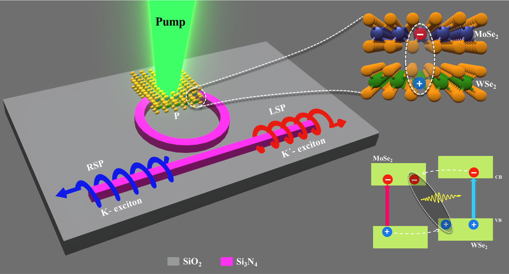
Introduction –Van der Waals heterostructures (vdWH) of atomically thin semiconductors[1] such as transition metal dichalcogenides (TMDCs) have proven to be an effective platform for designing nano and micro-scale optoelectronic and photonic devices for a variety of applications ranging from quantum information processing [2, 3, 4, 5, 6, 7] to valleytronics-based devices[8, 9, 10, 11, 12]. One promising feature of these heterostructures is their ability to host excitons with large binding energies[12]. These excitons exhibit various transition dipole moments[13] facilitating a rich diversity of their coupling with various types of optical modes[14, 15, 16]. Interlayer excitons[17], formed due to the type II band alignment in these heterobilayer structures (shown in the insets of Figure 1), have recently gained attention due to their longer radiative lifetimes (20–30 ns) [18] and smaller scattering rates [19], making such excitons well suited candidates for applications such as quantum information processors and valleytronic devices.
For valleytronics applications, the peculiar optical selection rules for valley excitons ( or ) of both TMDC monolayers in the vdWH material [20, 21, 22, 23, 24, 25] are extremely important. For example, in monolayers, spin-singlet excitons formed in these valleys couple to in-plane circularly polarised photons, resulting from their in-plane transition dipole moment. While their counterpart, spin-triplet excitons, have a weaker dipole transition and couple to linearly polarised photons in the out-of-plane direction. In vdWHs, both spin-singlet and spin-triplet valley excitons can couple with right-handed () and left-handed () circularly polarized and linearly polarized light[23, 26]. The transition dipole moments of these excitons in vdWHs can be tuned through external electric and magentic fields[27, 28, 29] or through interlayer translation i.e. based on their atomic registry in different stacking arrangement triangular R-type stacking or hexagonal H-type stacking ([30, 31]) of vdWH [25]. As an example, Sohoni et al. [32] show circularly polarised orthogonal interlayer valley excitonic dipoles in vdWH vertical heterostructure. These interlayer excitons have a tilted quantization axis in both R-type and H-type stacking for certain values of the translation between the two layers. In general, the dipole moments for interlayer valley excitons in the valleys can be expressed as
| (1) |
| (2) |
where and , depending on the stacking (R/H), , and . The coefficients are dependent on the lateral shift between the monolayers forming the heterostructure. We consider only those cases where the dipoles in the two valleys are orthogonal, that is, . While commensurate TMDC bilayer heterostructures with most of the interlayer translation values, do not exist naturally, they can be found in incommensurate heterostructures with small twist angles (moire superlattices) [33, 34]. These Moiré superlattices also generate an array of such interlayer excitons and thus, have the potential to host interacting quantum emitter arrays which has enormous potential for information processing [35, 36, 37, 38]. However, optically addressing these excitons is a challenge in free space setups due to their out of plane transition dipole moments[39] and on chip scale due to the weak evanescent overlap in under-optimized structures. This can be overcome by using near field coupling to the optical modes of nanophotonic architectures[39, 40, 41, 42, 43, Liu2019]. The ‘non-trivial’ tilted circularly polarized transition dipoles result in highly versatile and rich coupling dynamics with such nanophotonic platforms, which can be further tuned by varying the configuration of the bilayer stacking as well as the choice of initial valley excitation[32].
Separation of valley excitons in TMDC monolayers has so far been implemented via plasmonic nanostructures [45, 46], dielectric antennae and nanowires[47, 48] and photonic crystals[49, 50]. To the best of our knowledge, there has been no previous work on valley routing for interlayer excitons coupled to nanophotonic architectures. In this letter, we propose a dielectric microcavity – - microresonator platform for efficient valley selective separation and routing of interlayer excitons in bilayer heterostructures. Si3N4 based photonic integrated circuits (PIC) are a fully planar platform which are compatible with complementary metal–oxide–semiconductor (CMOS)-technology[51] and show extremely low loss in the whole visible to infrared spectrum [52]. We employ bus waveguide for routing and based microring resonator (MRR) as a cavity, which belongs to the class of whispering gallery mode (WGM) type of microcavities, that typically trap photons (spatially and temporally) by re-circulating the resonant mode [53] and supports high quality factors (high-Q) [54].
In this work, we explore the coupling between interlayer excitons and -microring resonator/bus waveguide system in terms of coupling linewidth, transmission anisotropy, bilayer stacking configuration and polarized excitation for realistic design of interlayer exciton PIC platform. For this purpose, we study the transmission through a bus waveguide coupled to a Si3N4 microcavity with a vertically stacked vdWH TMDC integrated on top of the microcavity, using finite difference eigenmode solver (FDE) and three dimensional finite-difference-time-domain (3D-FDTD) simulations via commercially available Ansys Lumerical simulation software. We observe an asymmetric transmission at the bus waveguide end ports with changing helicity of the interlayer exciton dipole, thus opening avenues for a PIC platform for valley state routing and manipulation for interlayer excitons.
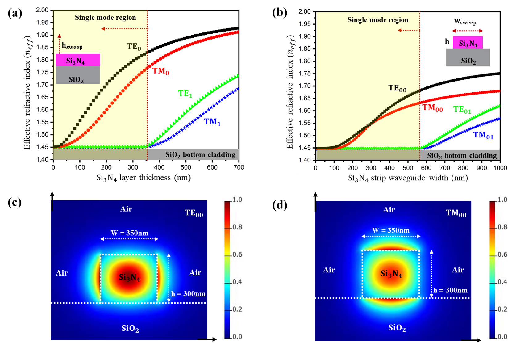
Designing single mode waveguides for interlayer excitonic PICs –
We first optimize our PIC platform for single mode operation for the bus waveguide and resonator. These single mode waveguides will help avoid competition with higher-order modes [55]. In our simulation set-up, the geometry consists of a strip-type waveguide with Si3N4 as the core material on top of a 2-m-thick silicon-di-oxide (SiO2) layer, acting as the bottom cladding layer to avoid the field leakage into the underlying Si-substrate. The standard Palik model [56] was used for SiO2 layer while the optical constant for Si3N4 was modelled using the Philipp model [57]. We carried out the modal analysis for R-type stacking excitonic dipole moment of emission wavelength at 908.48 nm. Firstly, the height of the waveguide was optimized using a one-dimensional finite difference eigenmode solver (1D-FDE) such that it supports only a single fundamental mode. Our simulation results indicate that the waveguide with a height up to 360 nm operates in the single mode regime as shown in the shaded region of Figure 2(a). For this work, we have therefore chosen the height of 300 nm for the waveguide. Secondly, waveguide width optimization was carried out by sweeping the waveguide width up to 1 m using two-dimensional 2D-FDE solver, keeping the height constant at 300 nm. For simplicity, the effective refractive index, , values till first order modes were measured. Figure 2(b) shows the effective refractive indices for the fundamental transverse electric quasi-TE00, transverse magnetic quasi-TM00, and the first order higher modes TE01, TM01. It can be clearly seen that for widths up to 560 nm, the waveguide exhibits only the fundamental quasi-TE00 and quasi-TM00 modes and this width also sets the cut-off for higher order modes (shown by vertical brown-dotted line in Figure 2(b)). Thus, we choose the single mode operational Si3N4 strip waveguide with a cross-sectional dimension of 300 nm 350 nm (). The cross-sectional mode field profiles of the fundamental quasi-TE00 and quasi-TM00 mode supported by the waveguide are depicted in Figure 2(c) and (d).
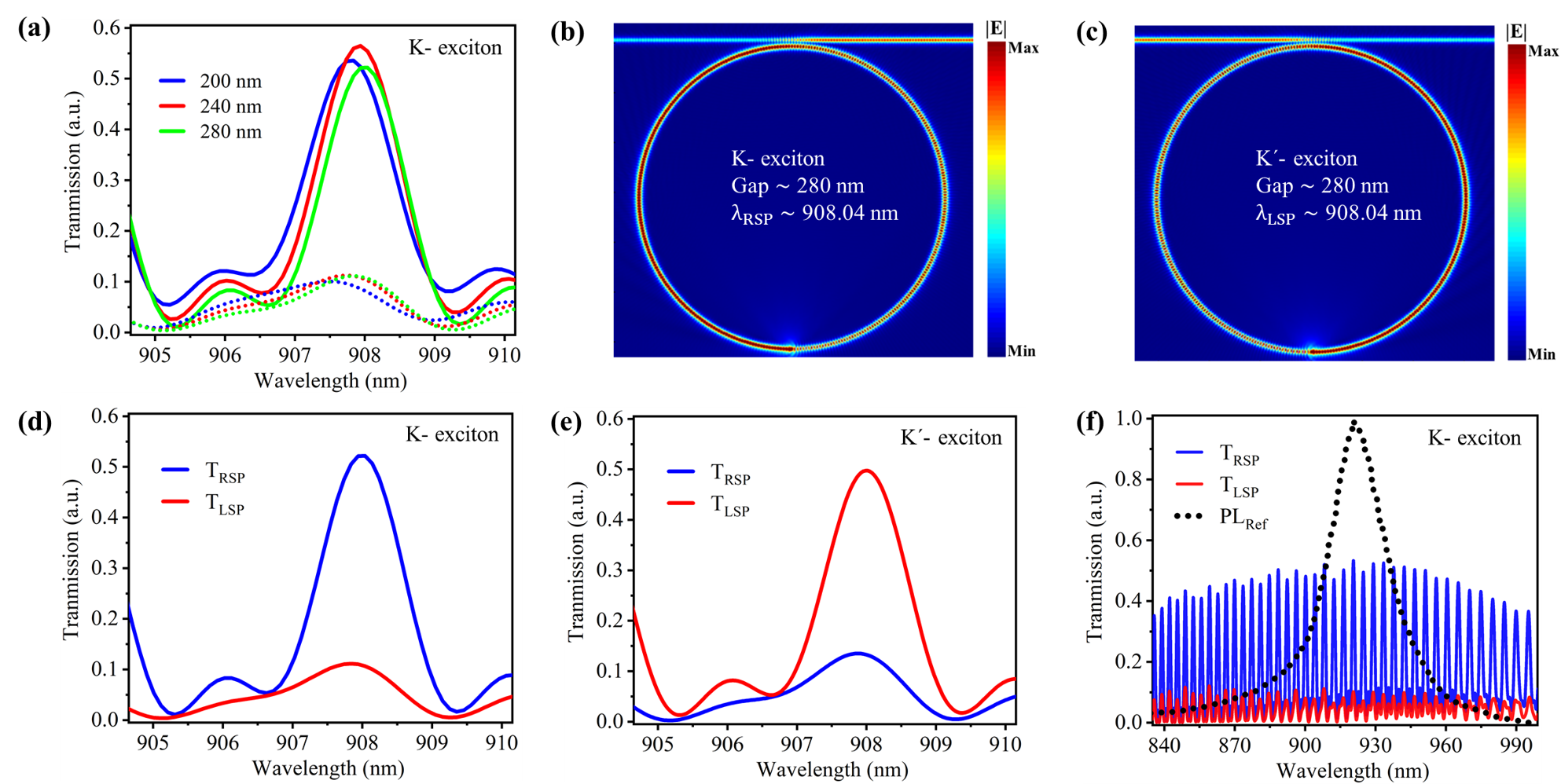
Engineered asymmetry for excitonic emission– The valley dependent asymmetric transmission of emitted photons from the interlayer exciton recombination was studied using 3D FDTD simulations where, a hybrid integration of stacked monolayers of and vdWH TMDCs was kept on top of Si3N4 microring resonator coupled to a bus-waveguide geometry was considered. The vdWH was placed at a symmetric position, marked as on the Si3N4 ring of 30 m diameter as shown in Figure 1. A 30 m diameter of the ring was chosen to minimize the bending losses in the propogating cavity-coupled modes and to obtain free spectral range FSR of nm for the resonant mode at wavelength 908.48 nm and n = 2 refractive index of Si3N4. The interlayer valley exciton formed in the TMDC stack was modelled as an electric dipole, which also acts as the optical point source for exciting the system. In the main text, we have presented the detailed analysis of the first spin-singlet R-type stacking configuration of excitonic transition dipole having 908.48 nm emission wavelength. The analysis for remaining dipoles is presented in the supplementary information.
The interlayer valley exciton emission is coupled to the Si3N4 MRR and propagates in both clockwise and counter-clockwhise direction inside the cavity from the originating point as is shown in Figures 3(b) and (c). For the valley exciton emitting at 908.48 nm, the counterclockwise propagating mode is relatively intense in comparison to the clockwise propagating mode as is clearly evident from the electric field () distribution profile shown in Figure 3(b), while for the corresponding valley exciton, clockwise propogating mode dominates, as shown in Figure 3(c). These clockwise and counterclockwise travelling modes get coupled out to the bus-waveguide across the gap between the bus and microring and are captured at the right-side port (RSP) and left-side port (LSP) of the bus-waveguide, respectively. For a quantitative analysis of the valley selective transmission response for all interlayer excitons, the maxima of the transmittance peak on both the ports should lie close to the emission wavelength of the dipole. It can be achieved by tuning the coupling gap between the microring resonator and the bus-waveguide. Figure 3(a) displays the fine tuning of the resonant transmission peak for the valley exciton at RSP and LSP ports by varying the coupling gap from 200 nm to 280 nm in steps of 40 nm. This can be attributed to coupling induced frequency shift[58]. The resonant peak for the 280 nm gap was found to be the closest to the targeted excitonic wavelength with a very small offset of nm and hence the gap was fixed to 280 nm for all subsequent analysis related to the 908.48 nm interlayer exciton. Figure 3(d) and (b) shows a pronounced difference in the mode intensity collected at the two end ports of the bus waveguide with RSP being stronger than the LSP for valley exciton. Figures 3(e and c) present a similar analysis for the conjugate dipole corresponding to valley exciton. Consequently, as the valley hosting the interlayer exciton is changed, the mode intensity or the transmittance at the two ports is also flipped yielding a highly directional separation and routing of the valley state.
To quantify the valley routing efficiency of the proposed system, the ratio of the area under the transmittance peaks (at the targetted excitonic emission wavelength) collected at the two ports was calculated. This ratio, from hereon referred to as “”, gives a measure of the efficiency of valley state routing. of and was obtained for the and valley excitons, respectively. Moreover, in accordance with the resonant condition for a cavity given by (where represents total optical path length, is effective refractive index, and is the resonant order of the cavity) [59], the microring resonator supports several resonant WGM peaks. The free spectral range (FSR) of the microcavity was estimated by simulating the transmission spectra over a wavelength span of 180 nm around the central wavelength (908.48 nm in this case) and was found to be 4.04 nm, in good agreement with the theoretical FSR calculation. Figure 3 shows the simulated transmission spectra for valley exciton, overlapped with the free-space photoluminescence (PL) for vdWH at room temperature as measured by Khelifa et al. [60]. It highlights that the room temperature PL envelops several cavity modes opening avenues for realizing cavity enhanced vdWH based light sources including nanolasers using our proposed platform.
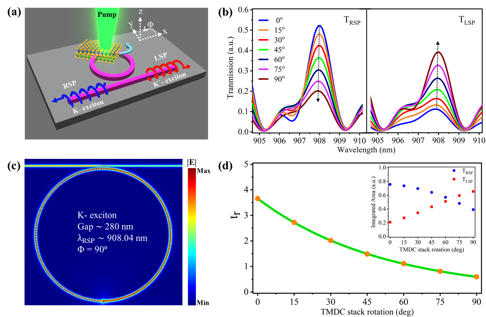
Effect of TMDC stack alignment on valley routing–
So far in this work, the TMDC stack orientation is considered to be aligned with the bus waveguide. However, in actual experiments, this condition might vary and affect the valley state routing efficiency of the device. Previously, Sigl et al. [61] have shown the effect of optical dipole orientation on the far-field emission of both H-type and R-type stacking configuration for vdWH at low-temperature. Therefore, to study the affect of orientation of TMDC stack in our system, we rotate the TMDC stack in plane, as shown in Figure 4(a). It is found that as the misalignment between the TMDC stack and x–axis (which coincides with the longer axis of the bus waveguide) is increased by rotating the stack from to , both forward and backward travelling modes get affected (see Figure 4 (b) and (d)), changing the transmission at the LSP and RSP ports of the bus waveguide. Consequently, the values drop significantly from 3.66 to 0.60 as shown in Figure 4(d). Additionally, we observe a complete flip in transmission at RSP and LSP ports (inset of Figure 4(d)), which is also evident from electric field () distribution shown in Figure 4(c). This suggests that our proposed system would also act as an efficient metrology tool to characterize the orientation of the vdWH stack on the ring waveguide.
Conclusion– In this paper, we propose a novel nanophotonic-hybrid device comprising interlayer excitons in vdWH TMDCs stack, coupled with Si3N4-microring resonator based PIC platform for efficiently routing the valley state. The heterobilayer TMDC stack can be monolithically integrated on the top of Si3N4-microring resonator at the symmetric position, which is coupled with bus waveguide. For efficient coupling, the waveguide was optimized to operate in single-mode condition. These interlayer excitons ( and valley) are circularly polarized with slighlty tilted quantization axes resulting in a highly directional and asymmetric transimission at the waveguide end ports for different valley states of the interlayer excitons. This valley routing phenomenon, quantified using , is also found to be strongly dependent on the orientation of the TMDC stack with respect to the bus-waveguide axis – a property which can enable our proposed system to act as a metrology tool for determining the orientation of the vdWH stack. This approach helps in valley selective routing of interlayer excitons, offering a CMOS compatible platform for future on-chip optoelectronic devices[6, 12, 5].
Acknowledgment– A.K. acknowledges funding support from the Department of Science and Technology via the grants: SB/S2/RJN-110/2017, ECR/2018/001485 and DST/NM/NS-2018/49.
References
- Novoselov et al. [2016] K. Novoselov, o. A. Mishchenko, o. A. Carvalho, and A. Castro Neto, 2d materials and van der waals heterostructures, Science 353, aac9439 (2016).
- Xu et al. [2014] X. Xu, W. Yao, D. Xiao, and T. F. Heinz, Spin and pseudospins in layered transition metal dichalcogenides, Nature Physics 10, 343 (2014).
- Reserbat-Plantey et al. [2021] A. Reserbat-Plantey, I. Epstein, I. Torre, A. T. Costa, P. A. D. Gonçalves, N. A. Mortensen, M. Polini, J. C. W. Song, N. M. R. Peres, and F. H. L. Koppens, Quantum nanophotonics in two-dimensional materials, ACS Photonics 8, 85 (2021).
- Baek et al. [2020] H. Baek, M. Brotons-Gisbert, Z. X. Koong, A. Campbell, M. Rambach, K. Watanabe, T. Taniguchi, and B. D. Gerardot, Highly energy-tunable quantum light from moiré-trapped excitons, Science Advances 6, 10.1126/sciadv.aba8526 (2020).
- Wilson et al. [2021] N. P. Wilson, W. Yao, J. Shan, and X. Xu, Excitons and emergent quantum phenomena in stacked 2d semiconductors, Nature 599, 383 (2021).
- Lin et al. [2021] K.-Q. Lin, P. E. F. Junior, J. M. Bauer, B. Peng, B. Monserrat, M. Gmitra, J. Fabian, S. Bange, and J. M. Lupton, Twist-angle engineering of excitonic quantum interference and optical nonlinearities in stacked 2d semiconductors, Nature Communications 12, 10.1038/s41467-021-21547-z (2021).
- Turunen et al. [2022] M. Turunen, M. Brotons-Gisbert, Y. Dai, Y. Wang, E. Scerri, C. Bonato, K. D. Jöns, Z. Sun, and B. D. Gerardot, Quantum photonics with layered 2d materials, Nature Reviews Physics 10.1038/s42254-021-00408-0 (2022).
- Ciarrocchi et al. [2022] A. Ciarrocchi, F. Tagarelli, A. Avsar, and A. Kis, Excitonic devices with van der waals heterostructures: valleytronics meets twistronics, Nature Reviews Materials 10.1038/s41578-021-00408-7 (2022).
- Schaibley et al. [2016] J. R. Schaibley, H. Yu, G. Clark, P. Rivera, J. S. Ross, K. L. Seyler, W. Yao, and X. Xu, Valleytronics in 2d materials, Nature Reviews Materials 1, 10.1038/natrevmats.2016.55 (2016).
- Vitale et al. [2018] S. A. Vitale, D. Nezich, J. O. Varghese, P. Kim, N. Gedik, P. Jarillo-Herrero, D. Xiao, and M. Rothschild, Valleytronics: Opportunities, challenges, and paths forward, Small 14, 1801483 (2018).
- Langer et al. [2018] F. Langer, C. P. Schmid, S. Schlauderer, M. Gmitra, J. Fabian, P. Nagler, C. Schüller, T. Korn, P. G. Hawkins, J. T. Steiner, U. Huttner, S. W. Koch, M. Kira, and R. Huber, Lightwave valleytronics in a monolayer of tungsten diselenide, Nature 557, 76 (2018).
- Mak et al. [2018] K. F. Mak, D. Xiao, and J. Shan, Light–valley interactions in 2d semiconductors, Nature Photonics 12, 451 (2018).
- Li et al. [2020] Z. Li, T. Wang, S. Miao, Z. Lian, and S.-F. Shi, Fine structures of valley-polarized excitonic states in monolayer transitional metal dichalcogenides, Nanophotonics 9, 1811 (2020).
- Chen et al. [2019] P. Chen, T. W. Lo, Y. Fan, S. Wang, H. Huang, and D. Lei, Chiral coupling of valley excitons and light through photonic spin–orbit interactions, Advanced Optical Materials 8, 1901233 (2019).
- Krasnok and Alù [2018] A. Krasnok and A. Alù, Valley-selective response of nanostructures coupled to 2d transition-metal dichalcogenides, Applied Sciences 8, 1157 (2018).
- Eswaramoorthy et al. [2022] L. Eswaramoorthy, S. Mokkapati, and A. Kumar, Engineering purcell factor anisotropy for dark and bright excitons in two dimensional semiconductors, Journal of Physics D: Applied Physics (2022).
- Rivera et al. [2018] P. Rivera, H. Yu, K. L. Seyler, N. P. Wilson, W. Yao, and X. Xu, Interlayer valley excitons in heterobilayers of transition metal dichalcogenides, Nature Nanotechnology 13, 1004 (2018).
- Palummo et al. [2015] M. Palummo, M. Bernardi, and J. C. Grossman, Exciton radiative lifetimes in two-dimensional transition metal dichalcogenides, Nano letters 15, 2794 (2015).
- Surrente et al. [2018] A. Surrente, Ł. Kłopotowski, N. Zhang, M. Baranowski, A. A. Mitioglu, M. V. Ballottin, P. C. Christianen, D. Dumcenco, Y.-C. Kung, D. K. Maude, et al., Intervalley scattering of interlayer excitons in a mos2/mose2/mos2 heterostructure in high magnetic field, Nano letters 18, 3994 (2018).
- Xiao et al. [2012] D. Xiao, G.-B. Liu, W. Feng, X. Xu, and W. Yao, Coupled spin and valley physics in monolayers of mos 2 and other group-vi dichalcogenides, Physical review letters 108, 196802 (2012).
- Mak et al. [2012] K. F. Mak, K. He, J. Shan, and T. F. Heinz, Control of valley polarization in monolayer mos 2 by optical helicity, Nature nanotechnology 7, 494 (2012).
- Cao et al. [2012] T. Cao, G. Wang, W. Han, H. Ye, C. Zhu, J. Shi, Q. Niu, P. Tan, E. Wang, B. Liu, et al., Valley-selective circular dichroism of monolayer molybdenum disulphide, Nature communications 3, 1 (2012).
- Wang et al. [2017a] G. Wang, C. Robert, M. M. Glazov, F. Cadiz, E. Courtade, T. Amand, D. Lagarde, T. Taniguchi, K. Watanabe, B. Urbaszek, et al., In-plane propagation of light in transition metal dichalcogenide monolayers: optical selection rules, Physical review letters 119, 047401 (2017a).
- Zeng et al. [2012] H. Zeng, J. Dai, W. Yao, D. Xiao, and X. Cui, Valley polarization in mos2 monolayers by optical pumping, Nature nanotechnology 7, 490 (2012).
- Yu et al. [2018] H. Yu, G.-B. Liu, and W. Yao, Brightened spin-triplet interlayer excitons and optical selection rules in van der waals heterobilayers, 2D Materials 5, 035021 (2018).
- Park et al. [2018] K.-D. Park, T. Jiang, G. Clark, X. Xu, and M. B. Raschke, Radiative control of dark excitons at room temperature by nano-optical antenna-tip purcell effect, Nature nanotechnology 13, 59 (2018).
- Peimyoo et al. [2021] N. Peimyoo, T. Deilmann, F. Withers, J. Escolar, D. Nutting, T. Taniguchi, K. Watanabe, A. Taghizadeh, M. F. Craciun, K. S. Thygesen, and S. Russo, Electrical tuning of optically active interlayer excitons in bilayer MoS2, Nature Nanotechnology 16, 888 (2021).
- Guo et al. [2021] H. Guo, X. Zhang, and G. Lu, Moiré excitons in defective van der waals heterostructures, Proceedings of the National Academy of Sciences 118, e2105468118 (2021).
- Tan et al. [2021] Q. Tan, A. Rasmita, S. Li, S. Liu, Z. Huang, Q. Xiong, S. A. Yang, K. S. Novoselov, and W. bo Gao, Layer-engineered interlayer excitons, Science Advances 7, 10.1126/sciadv.abh0863 (2021).
- Rosenberger et al. [2020] M. R. Rosenberger, H.-J. Chuang, M. Phillips, V. P. Oleshko, K. M. McCreary, S. V. Sivaram, C. S. Hellberg, and B. T. Jonker, Twist angle-dependent atomic reconstruction and moiré patterns in transition metal dichalcogenide heterostructures, ACS nano 14, 4550 (2020).
- He et al. [2021] F. He, Y. Zhou, Z. Ye, S.-H. Cho, J. Jeong, X. Meng, and Y. Wang, Moiré patterns in 2d materials: A review, ACS nano 15, 5944 (2021).
- Sohoni et al. [2020] M. Sohoni, P. K. Jha, M. Nalabothula, and A. Kumar, Interlayer exciton valleytronics in bilayer heterostructures interfaced with a phase gradient metasurface, Applied Physics Letters 117, 121101 (2020).
- Zhang et al. [2017] C. Zhang, C.-P. Chuu, X. Ren, M.-Y. Li, L.-J. Li, C. Jin, M.-Y. Chou, and C.-K. Shih, Interlayer couplings, moiré patterns, and 2d electronic superlattices in mos2/wse2 hetero-bilayers, Science advances 3, e1601459 (2017).
- Wang et al. [2017b] Y. Wang, Z. Wang, W. Yao, G.-B. Liu, and H. Yu, Interlayer coupling in commensurate and incommensurate bilayer structures of transition-metal dichalcogenides, Physical Review B 95, 115429 (2017b).
- Yu et al. [2017] H. Yu, G.-B. Liu, J. Tang, X. Xu, and W. Yao, Moiré excitons: From programmable quantum emitter arrays to spin-orbit–coupled artificial lattices, Science advances 3, e1701696 (2017).
- Seyler et al. [2019] K. L. Seyler, P. Rivera, H. Yu, N. P. Wilson, E. L. Ray, D. G. Mandrus, J. Yan, W. Yao, and X. Xu, Signatures of moiré-trapped valley excitons in mose2/wse2 heterobilayers, Nature 567, 66 (2019).
- Jin et al. [2019] C. Jin, E. C. Regan, D. Wang, M. Iqbal Bakti Utama, C.-S. Yang, J. Cain, Y. Qin, Y. Shen, Z. Zheng, K. Watanabe, et al., Identification of spin, valley and moiré quasi-angular momentum of interlayer excitons, Nature Physics 15, 1140 (2019).
- Wu et al. [2018] F. Wu, T. Lovorn, and A. MacDonald, Theory of optical absorption by interlayer excitons in transition metal dichalcogenide heterobilayers, Physical Review B 97, 035306 (2018).
- Tran et al. [2021] T. N. Tran, S. Kim, S. J. U. White, M. A. P. Nguyen, L. Xiao, S. Strauf, T. Yang, I. Aharonovich, and Z.-Q. Xu, Enhanced emission from interlayer excitons coupled to plasmonic gap cavities, Small 17, 2103994 (2021).
- Förg et al. [2019] M. Förg, L. Colombier, R. K. Patel, J. Lindlau, A. D. Mohite, H. Yamaguchi, M. M. Glazov, D. Hunger, and A. Högele, Cavity-control of interlayer excitons in van der waals heterostructures, Nature Communications 10, 10.1038/s41467-019-11620-z (2019).
- Rivera et al. [2019] P. Rivera, T. K. Fryett, Y. Chen, C.-H. Liu, E. Ray, F. Hatami, J. Yan, D. Mandrus, W. Yao, A. Majumdar, and X. Xu, Coupling of photonic crystal cavity and interlayer exciton in heterobilayer of transition metal dichalcogenides, 2D Materials 7, 015027 (2019).
- Khelifa et al. [2020a] R. Khelifa, P. Back, N. Flöry, S. Nashashibi, K. Malchow, T. Taniguchi, K. Watanabe, A. Jain, and L. Novotny, Coupling interlayer excitons to whispering gallery modes in van der waals heterostructures, Nano Letters 20, 6155 (2020a).
- Paik et al. [2019] E. Y. Paik, L. Zhang, G. W. Burg, R. Gogna, E. Tutuc, and H. Deng, Interlayer exciton laser of extended spatial coherence in atomically thin heterostructures, Nature 576, 80 (2019).
- Liu et al. [2019] Y. Liu, H. Fang, A. Rasmita, Y. Zhou, J. Li, T. Yu, Q. Xiong, N. Zheludev, J. Liu, and W. Gao, Room temperature nanocavity laser with interlayer excitons in 2d heterostructures, Science Advances 5, 10.1126/sciadv.aav4506 (2019).
- Sun et al. [2019] L. Sun, C.-Y. Wang, A. Krasnok, J. Choi, J. Shi, J. S. Gomez-Diaz, A. Zepeda, S. Gwo, C.-K. Shih, A. Alù, et al., Separation of valley excitons in a mos2 monolayer using a subwavelength asymmetric groove array, Nature Photonics 13, 180 (2019).
- Wen et al. [2020] T. Wen, W. Zhang, S. Liu, A. Hu, J. Zhao, Y. Ye, Y. Chen, C.-W. Qiu, Q. Gong, and G. Lu, Steering valley-polarized emission of monolayer MoS 2 sandwiched in plasmonic antennas, Science Advances 6, 10.1126/sciadv.aao0019 (2020).
- Gong et al. [2020] S.-H. Gong, I. Komen, F. Alpeggiani, and L. Kuipers, Nanoscale optical addressing of valley pseudospins through transverse optical spin, Nano Letters 20, 4410 (2020).
- Yao et al. [2021] Q. Yao, Y.-Q. Bie, J. Chen, J. Li, F. Li, and Z. Cao, Anapole enhanced on-chip routing of spin–valley photons in 2d materials for silicon integrated optical communication, Optics Letters 46, 4080 (2021).
- Wang et al. [2020] J. Wang, H. Li, Y. Ma, M. Zhao, W. Liu, B. Wang, S. Wu, X. Liu, L. Shi, T. Jiang, and J. Zi, Routing valley exciton emission of a WS2 monolayer via delocalized bloch modes of in-plane inversion-symmetry-broken photonic crystal slabs, Light: Science & Applications 9, 10.1038/s41377-020-00387-4 (2020).
- Peng et al. [2020] R. Peng, C. Wu, H. Li, X. Xu, and M. Li, Separation of the valley exciton-polariton in two-dimensional semiconductors with an anisotropic photonic crystal, Phys. Rev. B 101, 245418 (2020).
- Subramanian et al. [2013] A. Z. Subramanian, P. Neutens, A. Dhakal, R. Jansen, T. Claes, X. Rottenberg, F. Peyskens, S. Selvaraja, P. Helin, B. DuBois, K. Leyssens, S. Severi, P. Deshpande, R. Baets, and P. V. Dorpe, Low-loss singlemode PECVD silicon nitride photonic wire waveguides for 532–900 nm wavelength window fabricated within a CMOS pilot line, IEEE Photonics Journal 5, 2202809 (2013).
- Krückel et al. [2017] C. J. Krückel, A. Fülöp, Z. Ye, P. A. Andrekson, et al., Optical bandgap engineering in nonlinear silicon nitride waveguides, Optics express 25, 15370 (2017).
- Vahala [2003] K. J. Vahala, Optical microcavities, nature 424, 839 (2003).
- Xuan et al. [2016] Y. Xuan, Y. Liu, L. T. Varghese, A. J. Metcalf, X. Xue, P.-H. Wang, K. Han, J. A. Jaramillo-Villegas, A. Al Noman, C. Wang, et al., High-q silicon nitride microresonators exhibiting low-power frequency comb initiation, Optica 3, 1171 (2016).
- Han et al. [2018] H. Han, B. Xiang, and J. Zhang, Simulation and analysis of single-mode microring resonators in lithium niobate thin films, Crystals 8, 342 (2018).
- Palik [1998] E. D. Palik, Handbook of optical constants of solids, Vol. 3 (Academic press, 1998).
- Philipp [1973] H. R. Philipp, Optical properties of silicon nitride, Journal of the Electrochemical Society 120, 295 (1973).
- Li et al. [2009] Q. Li, M. Soltani, A. H. Atabaki, S. Yegnanarayanan, and A. Adibi, Quantitative modeling of coupling-induced resonance frequency shift in microring resonators, Optics Express 17, 23474 (2009).
- Bogaerts et al. [2012] W. Bogaerts, P. De Heyn, T. Van Vaerenbergh, K. De Vos, S. Kumar Selvaraja, T. Claes, P. Dumon, P. Bienstman, D. Van Thourhout, and R. Baets, Silicon microring resonators, Laser & Photonics Reviews 6, 47 (2012).
- Khelifa et al. [2020b] R. Khelifa, P. Back, N. Flory, S. Nashashibi, K. Malchow, T. Taniguchi, K. Watanabe, A. Jain, and L. Novotny, Coupling interlayer excitons to whispering gallery modes in van der waals heterostructures, Nano letters 20, 6155 (2020b).
- Sigl et al. [2022] L. Sigl, M. Troue, M. Katzer, M. Selig, F. Sigger, J. Kiemle, M. Brotons-Gisbert, K. Watanabe, T. Taniguchi, B. D. Gerardot, et al., Optical dipole orientation of interlayer excitons in mose 2- wse 2 heterostacks, Physical Review B 105, 035417 (2022).
- Lin [2021] K.-Q. Lin, A roadmap for interlayer excitons, Light: Science & Applications 10, 10.1038/s41377-021-00544-3 (2021).
- Mak and Shan [2018] K. F. Mak and J. Shan, Opportunities and challenges of interlayer exciton control and manipulation, Nature Nanotechnology 13, 974 (2018).