Topology optimization of dispersive plasmonic nanostructures in the time-domain
Abstract
Topology optimization techniques have been applied in integrated optics and nanophotonics for the inverse design of devices with shapes that cannot be conceived by human intuition. At optical frequencies, these techniques have only been utilized to optimize nondispersive materials using frequency-domain methods. However, a time-domain formulation is more efficient to optimize materials with dispersion. We introduce such a formulation for the Drude model, which is widely used to simulate the dispersive properties of metals, conductive oxides, and conductive polymers. Our topology optimization algorithm is based on the finite-difference time-domain (FDTD) method, and we introduce a time-domain sensitivity analysis that enables the evaluation of the gradient information by using one additional FDTD simulation. The existence of dielectric and metallic structures in the design space produces plasmonic field enhancement that causes convergence issues. We employ an artificial damping approach during the optimization iterations that, by reducing the plasmonic effects, solves the convergence problem. We present several design examples of 2D and 3D plasmonic nanoantennas with optimized field localization and enhancement in frequency bands of choice. Our method has the potential to speed up the design of wideband optical nanostructures made of dispersive materials for applications in nanoplasmonics, integrated optics, ultrafast photonics, and nonlinear optics.
keywords:
American Chemical Society, LaTeXLUH]Hannover Centre for Optical Technologies, Institute for Transport and Automation Technology (Faculty of Mechanical Engineering), and Cluster of Excellence PhoenixD, Leibniz University Hannover, 30167 Hannover, Germany
\alsoaffiliation[MNF]
Department of Electronics and Electrical Communications,
Menoufia University, Menouf 32952, Egypt
\alsoaffiliation[UMU]
Department of Applied Physics and Electronics,
Umeå University, SE-901 87 Umeå, Sweden
LUH]Hannover Centre for Optical Technologies, Institute for Transport and Automation Technology (Faculty of Mechanical Engineering), and Cluster of Excellence PhoenixD, Leibniz University Hannover, 30167 Hannover, Germany
\abbreviationsIR,NMR,UV
1 Introduction
The last decade has witnessed an exponential increase of research in nanophotonics. Plasmonic and dielectric nanostructured materials, such as metasurfaces and metamaterials, have been developed to engineer the properties of light beyond what is allowed by bulk optical devices1, 2, thus leading to revolutionary solutions for beam structuring3, colouring4, biosensing5, nanomedicine6, tunable beam steering7, and nonlinear generation8, 9, to name a few. Advances in nanofabrication technologies have enabled such technologies by allowing unprecedented design complexity at the nanoscale10, 5. The opportunities offered by theoretical research and nanofabrication facilities raise the need for new methods to efficiently design and optimize such nanophotonic systems11, 12.
Advances in computing capabilities and numerical methods, such as the finite-difference time-domain (FDTD)13 and finite-element methods (FEM)14, empowered the design of nanophotonic devices while shortening their design cycle. Conventionally, a design cycle starts from a given layout. The layout is then parameterized and various techniques are employed to explore the parameters’ space to find satisfying solutions. The use of large parameter spaces offers opportunities to find new designs with improved performance or designs that can satisfy multi-objectives. However, exploring such large parameter spaces raises computational challenges. Techniques such as parameters sweep or stochastic optimization methods, e.g., genetic algorithms, are computationally intractable to explore large design spaces and are only suitable to handle problems with few design parameters15. Deep learning algorithms require large data sets for training, and their use in the inverse design of nanophotonics is still in its infancy16, 17, 18.
Topology optimization (TopOpt) is a robust inverse design approach19, 20. It was initially introduced to optimize mechanical structures21, then it has been successfully extended to various engineering disciplines including acoustics22, fluids23, and electromagnetics24, 25, 26, 27, 28. Typically, TopOpt problems are solved using gradient-based optimization methods, where the gradient of the objective function is computed using efficient methods such as the adjoint-field method29, 30. Optimization problems that include millions or even billions of design variables have enabled novel conceptual designs31. In electromagnetics, TopOpt was used to optimize non-dispersive dielectric devices in the microwave and optical regimes32, 33, 34, 35. In addition, it was used to design plasmonic antennas using frequency-domain methods36, 37, 38. Christiansen et al.37 proposed a non-linear interpolation scheme that was successful to enable TopOpt of plasmonic antennas near their surface plasma frequency using the FEM method.
Structural perturbations or changes in material properties, caused for example by fabrication tolerance or temperature variations, raise the demand to account for the broadband performance of optical components39. At optical and near-infrared wavelengths, various materials exhibit dispersion, that can be modelled via Drude, Lorentz, or critical-points functions13, 40, 41. Below their plasma frequency, the Drude model is commonly used to describe the dispersive properties of metals such as silver, gold, and aluminum42. The model also describes the permittivity of conductive oxides, such as indium tin oxide (ITO)43, and conductive polymers44, including their dielectric and epsilon-near-zero regions.
In this paper, we introduce TopOpt of dispersive optical materials in the time-domain and aim at broadband designs. We base our algorithm on the FDTD method13 and the Drude model to describe the material dispersion. To the best of our knowledge, this is the first time the FDTD method is used for TopOpt of plasmonic devices in the time domain. To present the algorithm, we conduct the optimization of plasmonic nanoantennas, with the goal to maximize the electric energy in a specified region by finding the distribution of the electric permittivity in a design domain. To evaluate the gradient of the objective function efficiently, we employ the adjoint-field method and provide sensitivity analysis based on Maxwell’s equations in their first-order form. During the optimization, the interpolation of the design material between dielectric and metal enables the surface plasmon frequency to develop inside the frequency band of interest45, 46. Plasmonic effects, such as field localization and enhancement, are amplified close to . This leads to hot-spots within the optimization domain that prevent the algorithm from converging to well performing designs. To overcome these convergence issues, we exploit the conductivity term in Maxwell’s equations to introduce an artificial damping. This damping counteracts the high-field localization during the optimization process and enables the algorithm to converge to good designs. The developed algorithm is demonstrated by optimizing 2D (TM and TE) and 3D silver nanoantennas operating near plasma and infrared frequencies. In all cases, the algorithm produces novel designs with outstanding performance, which demonstrates its potential to offer new opportunities for optimizing dispersive optical nanostructures and metamaterials.
2 Optimization problem setup
In this section, we present the setup of the optimization problem that will be used to inverse design 2D and 3D nanostructures. The computational domain consists of , as shown in Fig. 1(a). The domain is an observation region where the electric energy is to be maximized. We assume that is a dispersionless dielectric medium with relative permittivity and has an area . Inside the design domain , we aim to distribute a dispersive material to form the nanoantenna structure. We consider materials with relative permittivity described by the Drude model:
| (1) |
where is the high-frequency permittivity; is the collision rate; is the square of the plasma frequency; is the vacuum permittivity; , , and are the electrons’ density, effective mass, and charge, respectively. We use the convention.
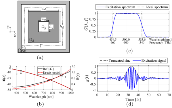
In this paper, we consider silver in the wavelength range – nm, where we fit its measured complex permittivity, adapted from McPeak et al.47, via a Drude model with parameters , rad/s, and rad/s, as shown in Fig. 1(b). The background space hosts the design domain , and has a constant relative permittivity . For simplicity, we use , but deviation from these values is also possible. The computational domain is terminated by perfectly matched layers . In our analysis, we use the total-field scattered-field formulation13 to inject a plane-wave through the boundary , which is located in . A similar setup was previously used to optimize TM nanoantennas with frequency-domain methods36, 37.
To optimize in the time-domain, the spectral content of the excitation signal determines the desired bandwidth of the structure under optimization. Ideally, we would like to excite the system with a signal that has a rectangular spectrum (see Fig. 1(c)). Unfortunately, this corresponds to a sinc signal of infinite duration. Thus, in order to keep the simulation time reasonable, the sinc signal is truncated to a few lobes, as shown in Fig. 1(d). Such signal modulates a carrier with a frequency corresponding to the center of the spectral window of interest. In addition, we use a Hanning window to reduce the ripples in the excitation spectrum. This processing results in rounding the edges of the spectral window.
We formulate the conceptual optimization problem
| (2) | ||||
| subject to: | the governing equations, | |||
| and a specified spectral content, |
where
| (3) |
is the electric energy in , is the time-dependent electric field, and is the observation time. The statement of the optimization problem is to find, for each point in , the permittivity distribution that maximizes the electric energy in subject to a specified excitation spectrum. The domain corresponds to the gap of a plasmonic nanoantenna where the incoming field is to be enhanced, or to a focus region where the energy is collimated by the designed structure. A detailed description of the numerical treatments of the optimization problem, including the sensitivity analysis and the numerical solution, is given in the Methods section.
2.1 Density-based interpolation and convergence issues
In density-based topology optimization, we use the permittivity function of the material as our design variable. For each point in we want the permittivity at that point to be either that of the Drude material or that of the background space . In order to interpolate between the background space and the design material, a density variable is introduced to describe the material at each edges of the computational grid in . The vector is used to hold the design variables of the optimization problem. Since we aim to use gradient-based methods to solve the topology optimization problem, the entries of the design vector are allowed to attain values between and during the optimization process. However, to obtain a manufacturable design, the final density vector must hold only the binary values or . We map each design variable to the physical material parameters using the following interpolation scheme:
| (4) |
where
| (5a) | ||||
| (5b) | ||||
| (5c) | ||||
are our three design variables (the dependence on is carried by the subscript). The parameters and perform a linear interpolation between the physical parameters of the background space and those of the design material . We use to ensure , thus avoiding the singularity in Eq. (21). In fact, the value corresponds to the Drude model , and sufficiently approximates the background space permittivity . To overcome convergence issues, we modify the Drude model to include an artificial conductivity , that plays a temporary role only during the optimization. In order to do so, we use a parabolic profile, so that the conductivity is zero for and , and reaches its maximum value for . The value must be carefully chosen, as discussed later. Fig. 2(a)-(c) show the interpolation between the permittivity of free space () and silver () using the design permittivity model in Eq. (4), where we drop the index for brevity.
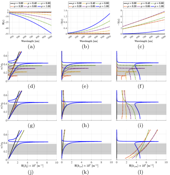
The presence of metal and dielectric in the design domain leads to localization and enhancement of the electric field due to surface plasmon modes arising during the optimization process. This hinders the convergence of the objective function. To understand the reason for such convergence problem, we use, as an illustrative model, the dispersion relation of surface plasmon polaritons (SSPs) at a flat interface between a dielectric and our design material 45, 46:
| (6a) | ||||
| (6b) | ||||
| (6c) | ||||
where is the propagation constant parallel to the interface; and are attenuation factors normal to the interface inside the dielectric and metal, respectively; and , as shown in Figs. 2(d)-(f) for values of between air () and silver (). The horizontal gray strip marks the wavelength interval of interest – nm. Inspecting the silver case (), we see that the value of reaches a maximum close to the surface plasmon frequency 45, 46, which by design is located outside the wavelength window of interest. The values of and also reach a maximum close to , which indicates a large wave attenuation in the directions normal to the interface. In other words, the wave propagates with the wavenumber , and it is spatially highly localized at the interface region. The range of frequencies is not of interest for SPPs. For intermediate values of , the material permittivity changes from metal to dielectric, and moves across the wavelength window of interest. This results in moving the peaks of the dispersion curves into the wavelength window of interest, as shown in Figs. 2(d)-(f) for S/m. The high-field localization, associated with large amplitudes of , and , counteracts the objective function that aims to maximize the electric field in the domain . This conflict prevents the algorithm from converging to well-performing designs.
With the aim to reduce the peaks in the dispersion diagrams at intermediate values of , we estimate the value of based on a parameter sweep, as shown in Figs. 2(g)-(i) for S/m. We note that a too-large value of leads to an intermediate material with conductivity higher than silver, as shown in Fig. 2(l) for S/m, thus causing less wave penetration inside the material. A too-large value of prevents the algorithm from converging to black and white designs since the structure becomes less lossy for such a value, while a too-small value is not enough to introduce sufficient damping to counteract the plasmonic effects.
3 Methods
3.1 Governing equations and sensitivity analysis
Inside the computational domain, that we assume source-free and non-magnetic with vacuum permeability , the time-dependent electric field and magnetic field are governed by Maxwell’s equations
| (7a) | |||
| (7b) | |||
where the electric displacement field models the optical response of the materials through the frequency domain relation
| (8) |
In our case, we use the design permittivity model
| (9) |
that consists of a Drude model and an additional artificial conductivity term that operates only during the optimization process to guarantee convergence.
By substituting Eq.(9) and Eq.(8) into Eq.(7a), we rewrite the time-domain Maxwell’s equation (7) as
| (10a) | |||
| (10b) | |||
| (10c) | |||
where the dispersion of the medium is embedded in the polarization current density , with Eq.(10b) being the time-domain equivalent of
| (11) |
We solve the design problem by using a gradient-based optimization method. To do so, we need derivatives of the objective function with respect to the design variables , , and . In this section, we use the adjoint-field method to derive expressions for such derivatives.
Assuming that the design variables are perturbed by , , and , the corresponding first variations of are
| (12a) | |||
| (12b) | |||
| (12c) | |||
To find explicit expressions for (12), we use the system governing equations (10) and employ the adjoint-field method29, 30. In the following, we derive an explicit relation for . To simplify the derivation, we drop the domain and consider as the external boundary of the analysis domain , see Fig. 1(a). In addition, we drop the differential and since they can be inferred from the limits of the integrals. We consider the initial-boundary-value-problem,
| (13a) | ||||
| (13b) | ||||
| (13c) | ||||
| (13d) | ||||
| (13e) | ||||
where is the intrinsic impedance of the domain , and with denoting the outward unit normal at . The boundary condition (13d) is used to impose an incoming excitation through . To simplify the notation, the symbol is temporarily used to denote the perturbation of the fields with respect to . We differentiate the system of equations (13) with respect to ,
| (14a) | ||||
| (14b) | ||||
| (14c) | ||||
| (14d) | ||||
| (14e) | ||||
We define the adjoint fields , , and . We perform the scalar product of (14a), (14b), and (14c) with , , and , respectively. We add the result of multiplication, integrating over the whole analysis domain and the observation interval , and applying integration by parts, we obtain
| (15) |
We assume that the adjoint fields satisfy the terminal conditions at . By arranging the terms in (3.1), utilizing (14d), and adding and subtracting , we obtain
| (16) |
If we require
| (17a) | ||||
| (17b) | ||||
| (17c) | ||||
| (17d) | ||||
| (17e) | ||||
then equation (3.1) reduces to
| (18) |
Expression (18) is the directional derivative of when is perturbed by . The gradient of with respect to can be identified as the integral kernel
| (19) |
The adjoint system (17) is a terminal-value-problem which, by changing the time variable (i.e., ) and the sign of the magnetic field (i.e., to preserve the direction of the Poynting vector), can be written as
| (20a) | ||||
| (20b) | ||||
| (20c) | ||||
| (20d) | ||||
| (20e) | ||||
and (19) becomes
| (21) |
where is the electric field of the forward system (13) reversed in time. The singularity of (21) can be avoided by ensuring the condition . The only difference between the adjoint system (20) and the forward system (13) is the source. In the forward system (13), the source is a plane-wave imposed through the boundary , see (13d). In the adjoint system (20), the source is the time-reversal of the forward electric field monitored at .
By differentiating system (13) with respect to and , and following similar procedures as before, we obtain the same adjoint system (20) and the following gradient expressions
| (22) |
and
| (23) |
Therefore, to evaluate the gradient components of the objective function, we solve the forward system (13) and the adjoint system (20), then we use (21), (22), and (23) to form the full gradient components.
3.2 Numerical treatments and optimization algorithm
We solve numerically the system of governing equations, discussed in the previous section, using the FDTD method13. We adopt the auxiliary differential equation approach to implement the Drude model in the FDTD method, and the uniaxial perfectly matched layer (UPML) is used to simulate the open-space radiation boundary condition40, 13. The computational domain is discretized into uniform square (2D) or cubical (3D) Yee cells with spatial steps in all Cartesian directions, and the total-field scattered-field approach is used to impose the plane-wave excitation.
In the forward system, we use the FDTD method and discretize the electric field at full-time indices and the magnetic field at half-time indices. In the adjoint system, however, the FDTD discretization of the electric- and magnetic fields are performed at half-time indices and full-time indices, respectively25, 30. The discretized objective function is
| (24) |
where is the discretized electric field at time index , is the FDTD’s temporal discretization step, and is the number of time steps used in the simulations. Based on the FDTD discretization of the forward and adjoint systems, the pointwise derivatives of the gradient expressions given in Section 3.1, are
| (25a) | ||||
| (25b) | ||||
| (25c) | ||||
where denotes the index of the edge in the design domain. Note that the temporal averaging of the discrete adjoint fields in (25a) and (25c) is related to the time shift between the forward and the adjoint discrete systems30.
To avoid mesh-dependency or self-penalization issues, in density-based topology optimization it is common to filter the design variables48, 49, 50, 51, 52. That is, instead of using in (5), we replace it with , where the filtered design vector is obtained through the mapping
| (26) |
In this work, we use an open-close, nonlinear filter operator that consists of a cascade of four -mean filters52. The filter has two tuning parameters that determine its size and the level of nonlinearity. Here, we fix the filter size to a constant value of and only employ the nonlinearity parameter to smoothly decrease the level of greyness in the design during the optimization process. More details about nonlinear filters and their use in topology optimization can be found in the literature52, 53. Using the chain rule, the derivative of the discrete objective function with respect to the design variable is evaluated by
| (27) |
We compared the derivatives computed using expression (27) against those evaluated by finite differences. The comparison showed more than digits match in precision between the two methods. We write the discrete version of the optimization problem as
| (28) | ||||
| subject to: | ||||
which we solve iteratively through the solution of a sequence of subproblems. Fig. 3 shows the flowchart of the optimization algorithm that we use to solve (28). To update the design variables, we use the globally convergent method of moving asymptotes (GCMMA)54. As a stopping criterion for the inner iteration loop, we monitor the norm of the first-order optimality condition after iterations. Then, we mark the decrease of this norm by % as the termination condition of the subproblem. For the termination of the outer loop, we monitor the decrease of the level of non-discreteness, with denoting a vector of a length and all entries equal one49. We terminate the optimization process either when the value of decreases below or a maximum number of iterations is reached. Then, the entries of the obtained design are thresholded around to yield the final design.

4 Results
In this section, we demonstrate the capabilities of the time-domain optimization method through several design examples of plasmonic nanostructures in 2D (TM and TE) and 3D. To enable fast simulation, we implement the FDTD method to execute on graphics processing units (GPUs). The computations are carried out on nodes equipped with NVidia V100 GPUs and 64 GB of memory. Based on the problem size, one call to the Maxwell solver uses a simulation time between less than a minute and a few minutes.
4.1 2D, TM nanoantennas
We chose a design domain with dimensions , and the observation domain is centered within and has dimensions , see Fig. 1(a). We use a space-step , and a time-step satisfying the Courant stability criterion. The simulation domain is truncated by 15 UPML cells placed 30 cells away from . The excitation is an polarized plane-wave propagating towards the positive axis. The excitation spectrum has a bandwidth of 20% at half-maximum and is centered at nm, as shown in Fig. 4(c) along with the results of optimization. The design variables are mapped to the in-plane permittivity components associated with the Yee edges where the electric field components and are located. Excluding the observation region, the design domain includes 79 560 design variables (edges).

Figure 4(a) shows the progress of the normalized objective function (see Eq. (24) in the Methods section) versus the iteration numbers. We start the algorithm with a uniform initial distribution for all design variables. Included in the same figure are some snapshots to show the development of the design. The black color indicates silver () and the white color indicates air (). Notably, the main topology of the antenna evolves after only a few tens of iterations. However, most of the late iterations are used to remove the intermediate material and form crisp boundaries, while the objective function keeps increasing monotonically. The increase of the objective function could be inferred from Fig. 2(i) as follows. The material interpolation between air and silver allows waves to penetrate deeper into materials with intermediate densities, and therefore, the energy losses inside the antenna structure increases. As the amount of intermediate material decreases, waves penetrate less inside the device structure which allows the objective function to increase. The design algorithm converged after iterations to a design with a grayness level % (see Methods section for the definition of ). We threshold this design around and show the final design, AntTM1, in Fig. 4(b). On the side facing the incident wave, the topology of AntTM1 developed as a flared horn, backed by a small cavity region. On the other side, we see two slightly tilted vertical arms. This optimized topology shares similarities with results reported in the literature using the FEM method37.
Fig. 4(c) shows the average field enhancement of AntTM1 at the observation domain , which correlates well with the spectrum of the excitation signal shown in the same figure. In the same figure, we cross-validate our computations with the commercial software package Ansys Lumerical FDTD55. Slight differences between the two computations are attributed to differences in geometry descriptions. Inside and within the main window of the excitation, AntTM1 exhibits more than -fold field enhancement compared to the incident wave. The peak of the performance, , occurs at the wavelength nm, which resides at long wavelengths in the excitation window. Figs. 4(d)-(j) show the electric field distribution of AntTM1 at four wavelengths, marked in Fig. 4(c). The electric field is maximum at the observation domain , marked by the box at the center. However, we observe a field localization and enhancement at the device’s boundaries for short wavelengths, which justifies the decrease of the energy enhancement in at short wavelengths. We attempt to improve the optimization results further by exploring three investigations in the following paragraphs.
4.1.1 Effect of the design domain size
The design obtained in Fig. 4 hits the boundary of the design domain, which suggests the need for a larger design space. We double the size of the design domain to nm2, and we solve the optimization problem, which now includes design variables. The algorithm used iterations to converge to the topology shown in Fig. 5(a). The new design, AntTM2, has more topological features compared to AntTM1. We observe an additional vertical arm that evolved in the rear-side of the device, and the arm around appears straight. The performance of AntTM2 has improved at short wavelengths, and it attains a nearly flat response within the excitation window, as shown in Fig. 5(b). Fig. 5(c) shows the field enhancement distribution of AntTM2 at the wavelength nm.
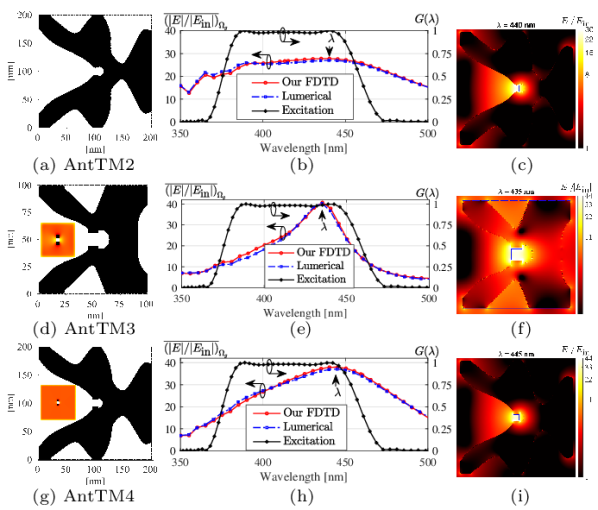
4.1.2 Effect of a fixed gap geometry
Maximizing the energy in suggests that the objective function is more sensitive to design variables close to compared to those away from it. We attempt to relax such a non-uniform distribution of the sensitivity and investigate its impact on the optimization results. We fix the geometry region below and above to silver with the same area as , and we solve the optimization problem. Figs. 5(d)-(f) and Figs. 5(g)-(i) show AntTM3 and AntTM4 which the algorithm produces when the design domain sizes nm2 and nm2 are used, respectively. For AntTM3 and AntTM4, fixing the area around the gap boosts the average field enhancement to a maximum value of and at the wavelength nm and nm, respectively; AntTM1 and AntTM2 have maximum values of and , respectively. The new nanoantennas exhibit better performances at long wavelengths, however, the performance at short wavelengths stays essentially the same as in the previous cases. These results indicate the challenges that plasmonic effects pose on optimizing nanoantennas near the surface plasmon frequency.
4.1.3 Wideband optimization
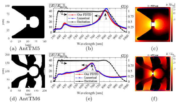
We combine the previous two investigations and pursue an attempt to optimize over a wider spectrum covering the wavelength window – nm. That is, we use an excitation signal with a half-maximum bandwidth of % centered around nm. Figs. 6(a)-(c) and Figs. 6(d)-(f) show the topology, the average field enhancement, and the field distribution at the wavelength of the maximum performance of the new designs. The new nanoantennas, called AntTM5 and AntTM6, show a wideband performance within the excitation spectrum. An average field enhancement above -fold is possible over the excitation window. Moreover, the average field enhancement hits a maximum of and at the wavelength nm and nm for AntTM5 and AntTM6, respectively. Here, we also observe the performance bias of the optimized nanoantennas towards long wavelengths. Further investigations are needed to improve the broadband performance.
4.2 2D, TE nanoantennas
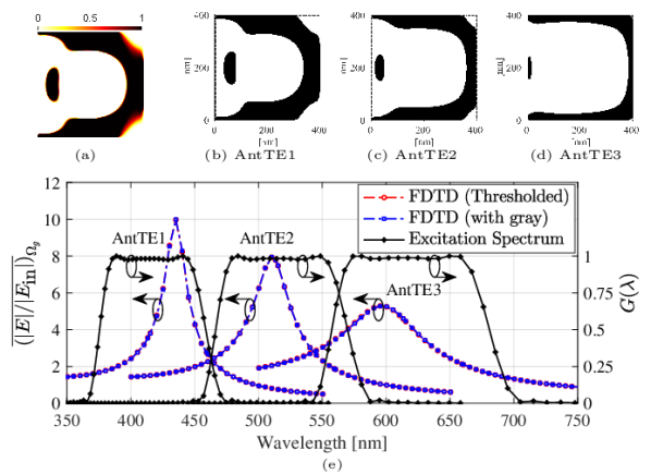
Surface plasmons develop at interfaces between metals and dielectrics only for TM polarization45, 46. Thus, plasmonic resonances in 2D structures are only possible for TM polarization. This suggests that the artificial damping is not needed for optimization under TE polarization (the excitation is an polarized plane wave), which is demonstrated in this section. Here, the design variables are assigned to the out-of-plane permittivity components associated with the electric field , see Fig. 1(a). We solve the optimization problem without using artificial damping. Our numerical experiments show a monotonic increase of the objective function, and the algorithm exhibit no convergence problems. For brevity, we do not include these numerical evidences here, and we only show the optimization results. Fig. 7 shows the optimization results of three nanoantennas optimized using three different excitation spectra. We refer to these nanoantennas as AntTE1, AntTE2, and AntTE3. For each design case, we shift the excitation spectrum by nm. This allows us to investigate the effect of the electric size on the optimization. For the three cases, we fix the size of the design domain nm2, the size of the observation domain nm2, and we use nm. A larger design domain was needed due to the absence of plasmonic resonances. In Fig. 7(a), we show the final design obtained by the algorithm for AntTE1. We notice that for the TE cases, the final designs contain small amounts of intermediate materials. We evaluate the performance of the optimized antennas before and after thresholding these intermediate materials, around . Fig. 7(e) shows that the performance of the antennas is not sensitive to such remaining intermediate material, which explains why they are not removed by the algorithm. For AntTE1, AntTE2, and AntTE3, the average field enhancement attains a maximum of , , and , and occurs at the wavelength nm, nm, and nm, respectively. The three structures have a paraboloidal shape reflector together with a standalone focusing segment, and the field enhancement is obtained as a result of a lensing effect, with being the focus. We remark that the absence of the plasmonic effects for the case of TE nanoantennas makes it hard to achieve field enhancement comparable to the TM nanoantennas with similar sizes. Also, we note that the larger the electric size of the design domain, the better the results the algorithm can achieve for TE waves.
4.3 3D antennas
As a final investigation, we use the developed method to optimize antennas in a 3D setup. We extend the problem model given in Fig. 1 to include a nm thickness in the -direction. The design space has a volume nm3 with nm3, and we use nm. Similar to the TM case, here we also fix the geometry region below and above to silver with the same area as . The discretized design domain includes design variables associated with its interior edges. Using smaller design volumes would require finer discretization steps and longer simulation times, which increases the demand for memory resources. We impose symmetry along the -axis to enable antennas producible by current technologies. That is, we optimize 3D antennas and aim for planar structures. The excitation is an polarized plane-wave propagating in the positive axis. We use the same setup and solve the optimization problem for three different wavelength excitation windows. The first and second excitation spectra, shown in Fig. 8(a), have a half-maximum bandwidth of % centered around nm and nm, respectively. The third excitation spectrum, shown in Fig. 8(b), has a half-maximum bandwidth covering the spectral window – nm. Each excitation spectrum results in a different topology which we name Ant3D1, Ant3D2, and Ant3D3, see Figs. 8(c)-(e). Interestingly, we observe the increase of the figure-of-eight void area of the three nanoantennas, around the observation domain , as the excitation spectrum includes long wavelengths. Fig. 8(f) shows the progress of the objective function and some snapshots of the intermediate designs for Ant3D1.
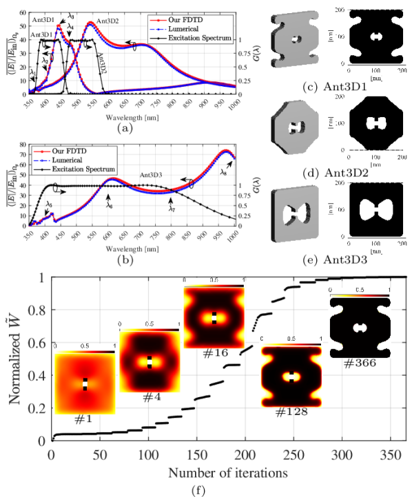
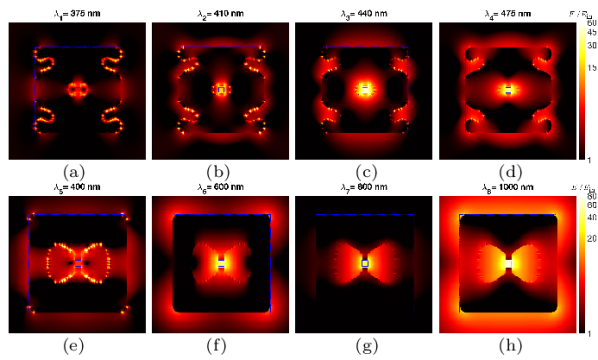
Fig. 8(a) shows the average field enhancement of Ant3D1 and Ant3D2, and Fig. 8(b) shows the performance of Ant3D3. Inside the observation domain , the nanoantennas Ant3D1, Ant3D2, and Ant3D3 exhibit a maximum average field enhancement of , , and at the wavelength nm, nm, and nm, respectively. Ant3D3 exhibits another peak of at nm, which resides slightly outside the intended excitation spectrum, near-infrared wavelengths. As in the 2D results, the optimized structures tend to exhibit a better field enhancement at long wavelengths. Compared to the TE case, the presence of the plasmonic effects in the TM and 3D cases enabled much smaller nanostractures. Figs. 9(a)-(d) and Figs. 9(e)-(h) show, respectively, the field distribution of Ant3D1 and Ant3D3 at some wavelengths, marked in Figs. 8(a)-(b). The optimized structures are capable to maximize the electric energy at the observation domain . At short wavelengths, however, we observe high-field localizations near their boundaries, which indicates strong plasmonic effects that are responsible for the decrease in the achieved performances. Similar to the 2D TM case, further investigations are needed to obtain a balanced performance over the wavelength window of interest.
5 Conclusion
We introduced a density-based topology optimization approach to design plasmonic dispersive nanoantennas. Our approach is based on Maxwell’s equations in the time-domain, and we use the Drude model, which can fit the material dispersion of metals and conductive polymers, as well as epsilon-near-zero materials, such as conductive oxides. For the TM and the 3D setups, the interpolation between metallic and dielectric phases results in high field-localization associated with plasmonic effects, which prevent the algorithm from converging to well-performing designs. Guided by dispersion diagrams of metal-dielectric interfaces, we proposed an artificial damping approach to suppress the field-localization during the optimization process, which enables the algorithm to converge to good designs. For the TE setup, artificial damping is not needed and the algorithm encounters no convergence issues. Various setups for narrowband and wideband optimization are presented, resulting in novel 2D and 3D nanoantenna designs with outstanding performances. Our method opens new opportunities for the automatic design and optimization of dispersive nanophotonic structures with broadband optical response for nanoplasmonics, nonlinear optics, epsilon-near-zero materials, ultrafast photonics, or integrated optics.
Acknowledgement
The computations were performed on resources provided by the Swedish National Infrastructure for Computing (SNIC) at HPC2N center; the central computing cluster operated by Leibniz University IT Services (LUIS); and the North-German Supercomputing Alliance (HLRN). A.C.L. acknowledges the Bundesministerium für Buldung und Furschung (German Federal Ministry of Education and Research) under the Tenure-Track Program, and the Deutsche Forschungsgemeinschaft (DFG, German Research Foundation) under Germany’s Excellence Strategy within the Cluster of Excellence PhoenixD (EXC 2122, Project ID 390833453).
References
- Yu et al. 2011 Yu, N.; Genevet, P.; Kats, M. A.; Aieta, F.; Tetienne, J.-P.; Capasso, F.; Gaburro, Z. Light Propagation with Phase Discontinuities: Generalized Laws of Reflection and Refraction. Science 2011, 334, 333–337
- Kamali et al. 2018 Kamali, S. M.; Arbabi, E.; Arbabi, A.; Faraon, A. A review of dielectric optical metasurfaces for wavefront control. Nanophotonics 2018, 7, 1041–1068
- Karimi et al. 2014 Karimi, E.; Schulz, S. A.; De Leon, I.; Qassim, H.; Upham, J.; Boyd, R. W. Generating optical orbital angular momentum at visible wavelengths using a plasmonic metasurface. Light Sci. Appl. 2014, 3, e167–e167
- Guay et al. 2017 Guay, J.-M.; Calà Lesina, A.; Côté, G.; Charron, M.; Poitras, D.; Ramunno, L.; Berini, P.; Weck, A. Laser-induced plasmonic colours on metals. Nat. Commun. 2017, 8, 16095
- Tseng et al. 2021 Tseng, M. L.; Jahani, Y.; Leitis, A.; Altug, H. Dielectric Metasurfaces Enabling Advanced Optical Biosensors. ACS Photonics 2021, 8, 47–60
- Baffou et al. 2020 Baffou, G.; Cichos, F.; Quidant, R. Applications and challenges of thermoplasmonics. Nature Materials 2020, 19, 946–958
- Calà Lesina et al. 2021 Calà Lesina, A.; Goodwill, D.; Bernier, E.; Ramunno, L.; Berini, P. Tunable Plasmonic Metasurfaces for Optical Phased Arrays. IEEE J. Sel. Top. Quantum Electron. 2021, 27, 1–16
- Lee et al. 2014 Lee, J.; Tymchenko, M.; Argyropoulos, C.; Chen, P.-Y.; Lu, F.; Demmerle, F.; Boehm, G.; Amann, M.-C.; Alù, A.; Belkin, M. A. Giant nonlinear response from plasmonic metasurfaces coupled to intersubband transitions. Nature 2014, 511, 65–69
- Calà Lesina et al. 2017 Calà Lesina, A.; Berini, P.; Ramunno, L. Vectorial control of nonlinear emission via chiral butterfly nanoantennas: generation of pure high order nonlinear vortex beams. Opt. Express 2017, 25, 2569–2582
- Rashid et al. 2021 Rashid, S.; Walia, J.; Northfield, H.; Hahn, C.; Olivieri, A.; Lesina, A. C.; Variola, F.; Weck, A.; Ramunno, L.; Berini, P. Helium ion beam lithography and liftoff. Nano Futures 2021, 5, 025003
- Molesky et al. 2018 Molesky, S.; Lin, Z.; Piggott, A. Y.; Jin, W.; Vucković, J.; Rodriguez, A. W. Inverse design in nanophotonics. Nat. Photonics 2018, 12, 659–670
- Campbell et al. 2019 Campbell, S. D.; Sell, D.; Jenkins, R. P.; Whiting, E. B.; Fan, J. A.; Werner, D. H. Review of numerical optimization techniques for meta-device design. Opt. Mater. Express 2019, 9, 1842–1863
- Taflove and Hagness 2005 Taflove, A.; Hagness, S. Computational Electrodynamics: The Finite-Difference Time-Domain Method, 3rd ed.; Artech House, 2005
- Jin 2014 Jin, J.-M. The finite element method in electromagnetics, 3rd ed.; Wiley, 2014
- Sigmund 2011 Sigmund, O. On the usefulness of non-gradient approaches in topology optimization. Struct. Multidiscip. Optim. 2011, 43, 589–596
- Baxter et al. 2019 Baxter, J.; Calà Lesina, A.; Guay, J.-M.; Weck, A.; Berini, P.; Ramunno, L. Plasmonic colours predicted by deep learning. Sci. Rep. 2019, 9, 8074
- Chen et al. 2020 Chen, Y.; Lu, L.; Karniadakis, G. E.; Negro, L. D. Physics-informed neural networks for inverse problems in nano-optics and metamaterials. Opt. Express 2020, 28, 11618–11633
- Ma et al. 2021 Ma, W.; Liu, Z.; Kudyshev, Z. A.; Boltasseva, A.; Cai, W.; Liu, Y. Deep learning for the design of photonic structures. Nat. Photonics 2021, 15, 77–90
- Bendsøe and Sigmund 2004 Bendsøe, M. P.; Sigmund, O. Topology Optimization; Springer Berlin Heidelberg, 2004
- Deaton and Grandhi 2014 Deaton, J. D.; Grandhi, R. V. A survey of structural and multidisciplinary continuum topology optimization: post 2000. Struct. Multidiscip. Optim. 2014, 49, 1–38
- Bendsøe and Kikuchi 1988 Bendsøe, M. P.; Kikuchi, N. Generating optimal topologies in structural design using a homogenization method. Comput. Methods Appl. Mech. Eng. 1988, 71, 197–224
- Wadbro and Berggren 2006 Wadbro, E.; Berggren, M. Topology optimization of an acoustic horn. Comput. Methods Appl. Mech. Eng. 2006, 196, 420–436
- Gersborg-Hansen et al. 2005 Gersborg-Hansen, A.; Sigmund, O.; Haber, R. Topology optimization of channel flow problems. Struct. Multidiscip. Optim. 2005, 30, 181–192
- Nomura et al. 2007 Nomura, T.; Sato, K.; Taguchi, K.; Kashiwa, T.; Nishiwaki, S. Structural topology optimization for the design of broadband dielectric resonator antennas using the finite difference time domain technique. Int. J. Num. Meth. Eng. 2007, 71, 1261–1296
- Hassan et al. 2014 Hassan, E.; Wadbro, E.; Berggren, M. Topology Optimization of Metallic Antennas. IEEE Trans. Antennas Propag. 2014, 62, 2488–2500
- Aage and Egede Johansen 2017 Aage, N.; Egede Johansen, V. Topology optimization of microwave waveguide filters. Int. J. Numer. Meth. Eng. 2017, 112, 283–300, nme.5551
- Wang et al. 2017 Wang, J.; Yang, X.-S.; Ding, X.; Wang, B.-Z. Antenna Radiation Characteristics Optimization by a Hybrid Topological Method. IEEE Trans. Antennas Propag. 2017, 65, 2843–2854
- Hassan et al. 2020 Hassan, E.; Scheiner, B.; Michler, F.; Berggren, M.; Wadbro, E.; Röhrl, F.; Zorn, S.; Weigel, R.; Lurz, F. Multilayer Topology Optimization of Wideband SIW-to-Waveguide Transitions. IEEE Trans. Microw. Theory Tech. 2020, 68, 1326–1339
- Zhang et al. 2014 Zhang, Y.; Ahmed, O. S.; Bakr, M. H. Wideband FDTD-Based Adjoint Sensitivity Analysis of Dispersive Electromagnetic Structures. IEEE Trans. Microw .Theory Tech. 2014, 62, 1122–1134
- Hassan et al. 2015 Hassan, E.; Wadbro, E.; Berggren, M. Time-Domain Sensitivity Analysis for Conductivity Distribution in Maxwell’s Equations; 2015
- Aage et al. 2017 Aage, N.; Andreassen, E.; Lazarov, B. S.; Sigmund, O. Giga-voxel computational morphogenesis for structural design. Nature 2017, 550, 84
- Jensen and Sigmund 2010 Jensen, J.; Sigmund, O. Topology optimization for nano-photonics. Laser Photonics Rev. 2010, 5, 308–321
- Elesin et al. 2014 Elesin, Y.; Lazarov, B.; Jensen, J.; Sigmund, O. Time domain topology optimization of 3D nanophotonic devices. Photonics Nanostructures: Fundam. Appl. 2014, 12, 23 – 33
- Frellsen et al. 2016 Frellsen, L. F.; Ding, Y.; Sigmund, O.; Frandsen, L. H. Topology optimized mode multiplexing in silicon-on-insulator photonic wire waveguides. Opt. Express 2016, 24, 16866–16873
- Augenstein and Rockstuhl 2020 Augenstein, Y.; Rockstuhl, C. Inverse Design of Nanophotonic Devices with Structural Integrity. ACS Photonics 2020, 7, 2190–2196
- Wadbro and Engström 2015 Wadbro, E.; Engström, C. Topology and shape optimization of plasmonic nano-antennas. Comput. Methods Appl. Mech. Eng. 2015, 293, 155–169
- Christiansen et al. 2019 Christiansen, R. E.; Vester-Petersen, J.; Madsen, S. P.; Sigmund, O. A non-linear material interpolation for design of metallic nano-particles using topology optimization. Comput. Methods Appl. Mech. Eng. 2019, 343, 23–39
- Zeng et al. 2021 Zeng, Z.; Venuthurumilli, P. K.; Xu, X. Inverse Design of Plasmonic Structures with FDTD. ACS Photonics 2021, 8, 1489–1496
- Giannini et al. 2011 Giannini, V.; Fernández-Domínguez, A. I.; Heck, S. C.; Maier, S. A. Plasmonic Nanoantennas: Fundamentals and Their Use in Controlling the Radiative Properties of Nanoemitters. Chem. Rev. 2011, 111, 3888–3912
- Okoniewaki et al. 1997 Okoniewaki, M.; Mrozowski, M.; Stuchly, M. Simple treatment of multi-term dispersion in FDTD. IEEE Microwave and Guided Wave Letters 1997, 7, 121–123
- Prokopidis and Zografopoulos 2013 Prokopidis, K. P.; Zografopoulos, D. C. A Unified FDTD/PML Scheme Based on Critical Points for Accurate Studies of Plasmonic Structures. J. Light. Technol. 2013, 31, 2467–2476
- Vial et al. 2005 Vial, A.; Grimault, A.-S.; Macías, D.; Barchiesi, D.; de la Chapelle, M. L. Improved analytical fit of gold dispersion: Application to the modeling of extinction spectra with a finite-difference time-domain method. Phys. Rev. B 2005, 71
- Alam et al. 2016 Alam, M. Z.; Leon, I. D.; Boyd, R. W. Large optical nonlinearity of indium tin oxide in its epsilon-near-zero region. Science 2016, 352, 795–797
- Karst et al. 2021 Karst, J.; Floess, M.; Ubl, M.; Dingler, C.; Malacrida, C.; Steinle, T.; Ludwigs, S.; Hentschel, M.; Giessen, H. Electrically switchable metallic polymer nanoantennas. Science 2021, 374, 612–616
- Raether 1988 Raether, H. Surface plasmons: on smooth and rough surfaces and on gratings; Springer: Berlin, 1988
- Maier 2007 Maier, S. A. Plasmonics: Fundamentals and Applications; Springer US: New York, NY, 2007
- McPeak et al. 2015 McPeak, K. M.; Jayanti, S. V.; Kress, S. J. P.; Meyer, S.; Iotti, S.; Rossinelli, A.; Norris, D. J. Plasmonic Films Can Easily Be Better: Rules and Recipes. ACS Photonics 2015, 2, 326–333
- Borrvall 2001 Borrvall, T. Topology optimization of elastic continua using restriction. Arch. Comput. Methods Engrg. 2001, 8, 351–385
- Sigmund 2007 Sigmund, O. Morphology-based black and white filters for topology optimization. Struct. Multidiscip. Optim. 2007, 33, 401–424
- Svanberg and Svärd 2013 Svanberg, K.; Svärd, H. Density filters for topology optimization based on the Pythagorean means. Struct. Multidiscip. Optim. 2013, 48, 859–875
- Hassan et al. 2014 Hassan, E.; Wadbro, E.; Berggren, M. Patch and ground plane design of microstrip antennas by material distribution topology optimization. Prog. Electromagn. Res. B 2014, 59, 89–102
- Hägg and Wadbro 2017 Hägg, L.; Wadbro, E. Nonlinear filters in topology optimization: existence of solutions and efficient implementation for minimum compliance problems. Struct. Multidiscip. Optim. 2017, 55, 1017–1028
- Hassan et al. 2018 Hassan, E.; Wadbro, E.; Hägg, L.; Berggren, M. Topology optimization of compact wideband coaxial-to-waveguide transitions with minimum-size control. Struct. Multidiscip. Optim. 2018, 57, 1765–1777
- Svanberg 2002 Svanberg, K. A Class of Globally Convergent Optimization Methods Based on Conservative Convex Separable Approximations. SIAM J. Optim. 2002, 12, 555–573
- 55 Ansys, Lumerical version 2020-2.4. \urlhttps://www.ansys.com/products/photonics/fdtd, Last accessed Dec. 2021