Intrinsic spin-valley locking for conducting electrons in metal-semiconductor-metal lateral hetero-structures of -transition-metal dichalcogenides
Abstract
Lateral-hetero structures of atomic layered materials alter the electronic properties of pristine crystals and provide a possibility to produce useful monolayer materials. We reveal that metal-semiconductor-metal lateral-hetero junctions of -transition-metal dichalcogenides intrinsically possess conducting channels of electrons with spin-valley locking, e.g., gate electrode. We theoretically investigate the electronic structure and transport properties of the lateral-hetero junctions and show that the hetero-structure produces conducting channels through the and valleys in the semiconducting transition-metal dichalcogenide and restricts the spin of the conducting electrons in each valley due to the valley dependent charge transfer effect. Moreover, the theoretical investigation shows that the hetero-junction of WSe2 realizes a high transmission probability for valley-spin locked electrons even in a long semiconducting region. The hetero-junction also provides a useful electronic transport property, a step-like I-V characteristic.
I Introduction
Atomic layered materials are solids consisting of atomically thin crystals stacked in layers. Modern experimental techniques enable one to produce atomically thin materials of the layers by cleaving from the bulk crystal, chemical vapor deposition,Lee et al. (2012); Bergeron et al. (2017), chalcogenationChen et al. (2017), or molecular-beam epitaxyMoreau et al. (2010); Zhan et al. (2017); El Kazzi et al. (2018). These thin layers have attracted much attention because of the fascinating electronic structures different from those of the bulk crystals.Castro Neto et al. (2009); Xiao et al. (2012) Moreover, the fabrication techniques to combine different layers into electric or optical systems have been developed in terms of application. Kang et al. (2013); Habe and Koshino (2015); Li et al. (2015); Najmzadeh et al. (2016); Son et al. (2016); Ullah et al. (2017) These atomically thin systems are expected for the realization of atomic layer electric circuits by combining different atomic layered materials.
Transition-metal dichalcogenides(TMDCs) are solid composed of transition-metal and chalcogen atoms, and include atomic layered materials in the -structure, a crystal structure of monolayer. In -monolayer crystals, electrons possess two degrees of freedom, spin and valley because of the crystal structure. The manipulation of spin and valley is one of the attractive purposes in the research field of atomic layered materials. Since the spin and valley are coupled due to Zeeman-type spin-orbit coupling in the monolayers, these materials are good candidates for these purposes.
The group VI transition-metal atoms, molybdenum and tungsten, form direct-gap semiconductors in structure with sulfur and selenium.Mak et al. (2010); Jin et al. (2013); Zhang et al. (2014) On the other hand, -crystals of niobium and tantalum, group V atoms, possess metallic properties including an anomalous superconductivity in NbSe2 showing fascinating phenomenaLu et al. (2015); Xi2016; Xi et al. (2016); Wang et al. (2017); Habe (2019a). In semiconducting -TMDCs, there is spin-valley locking of electrons in the and valleys but the charge injection is necessary to introduce conducting electrons via a gate electrode of FET, which breaks mirror symmetry of the crystal structure. Although the metallic -TMDCs intrinsically possess conducting channels for electrons, there are three valleys and no spin-valley correlation in the Fermi energy. Therefore, neither metallic nor semiconducting TMDCs possess conducting electrons with the spin-valley correlation intrinsically.
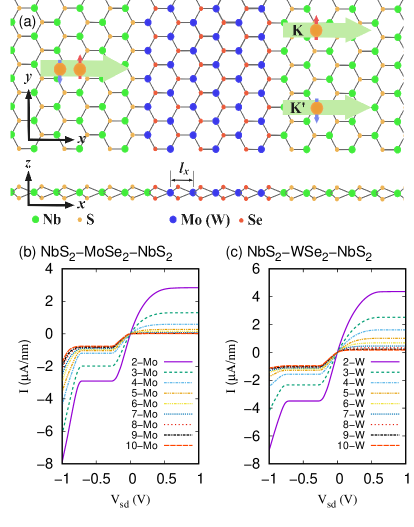
In this paper, we theoretically investigate the electronic structure and transport properties of metal-semiconductor-metal lateral hetero-junctions of -TMDCs, and show the hetero-junctions intrinsically provide the spin-valley locking to conducting electrons as shown in Fig. 1(a). Due to various electronic properties of -TMDCs, hetero structures of these monolayers have been studied for the application to electronic and optical devices in previous experimental papersLi et al. (2015); Lu et al. (2016); Son et al. (2016); Ullah et al. (2017) and theoretical papers.Sharma et al. (2014); Habe (2019b); Deilmann et al. (2020) The lateral-hetero structure is a single layer consisting of different atomic layers as a patchwork, and that of semiconducting -TMDCs has been realized experimentally with atomically aligned interfaces.Gong et al. (2014); Duan et al. (2014); Huang et al. (2014); Chen et al. (2015a, b); Li et al. (2015); Zhang et al. (2015); He et al. (2016); Najmzadeh et al. (2016) We consider the lateral-hetero structure of metallic and semiconducting TMDCs for providing a fascinating electronic system with spin-valley correlation. For investigating the electronic transport properties, a multi-orbital tight-binding model is introduced by referring to the first-principles band structures of the pristine monolayer and periodic stripe-lattice of two TMDCs. Moreover, the I-V characteristic of the junction is also theoretically calculated and shows that the hetero-junction provides step-like I-V characteristics, a fundamental function in conventional electronics, as shown in Figs. 1(b) and 1(c).
The remaining sections are organized as follows. In Sec. II, the crystal and electronic structures of monolayer NbS2, MoSe2, and WSe2 are discussed by using first-principles calculations. The electronic structure of s periodic lateral-hetero-structure is investigated in Sec. III. Moreover, a theoretical model is introduced for the study of electronic transport properties. In Sec. IV, the calculation method and numerical results of the electronic transport properties of metal-semiconductor-metal lateral-hetero-junctions of -TMDCs are provided. In Sec. V, we discuss the relation between the electronic structure and the electronic transport properties, and the effect of spin-valley locking on the transport phenomena. The conclusion is given in Sec. VI.
II Crystal and electronic structures of pristine monolayer crystals
Monolayer NbS2, MoSe2, and WSe2 are classified into 1-crystals and possess a honeycomb lattice structure consisting of three sublayers as shown in Fig. 2(a). In this section, the lattice parameters and electronic structure are presented for these materials by numerical calculations using the first-principles method. Although the electronic structure in a hetero-junction varies from that in each pristine crystal, the deviation decreases with increasing distance from the boundary of junction. The calculations are performed by using quantum-ESPRESSO, a package of numerical codes for density functional theory (DFT)Giannozzi et al. (2009), with the projector augmented wave method including spin-orbit coupling within generalized gradient approximation. The energy cut-off is 60Ry for the plane wave basis and 400Ry for the charge density. The convergence criterion 10-8 Ry is adopted for the self-consistent field calculation.
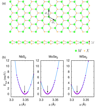
The lattice parameters of pristine crystals are estimated by comparing the total energy of electronic systems with different lattice parameters. The numerical results for NbS2, MoSe2, and WSe2 are presented in Fig. 2. In these calculations, the lattice constant of a honeycomb structure is considered as a parameter and the distance between the top and bottom sublayers is simultaneously optimized by the lattice relaxation code in quantum ESPRESSO. The numerical calculations show that the lattice constant of stable structure is almost the same among the three materials: 3.348 for NbS2, 3.324 for MoSe2, and 3.320 for WSe2 within 1%. The numerical results imply the feasibility of commensurate lateral hetero-structures composed of these layered materials with an aligned interface.
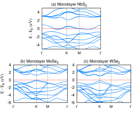
In Fig. 3, the first-principles band structures of pristine monolayers are presented by applying the optimized lattice parameters for NbS2, MoSe2, and WSe2. The first-principles results show the metallic character of NbS2 and the semiconducting character of MoSe2 and WSe2. In the semiconducting TMDCs, the top of the valence band splits at the point due to the Zeeman-type spin-orbit coupling where the heavier transition-metal atom W leads to a larger spin split. The energy dispersion is almost the same among these crystals due to the same crystal structure. In pristine MoSe2 and WSe2, the Fermi energy is inside the gap and indicates the absence of a conducting channel. In the lateral hetero junction, however, the connecting region of these materials can possess conducting channels due to the change of the band structure and the charge transfer through the interface.
III Electronic structure in lateral hetero-junction
In this section, electronic structures in lateral hetero-junctions are theoretically analyzed and a theoretical method is introduced for constructing a tight-binding model to investigate electronic transport properties of hetero-junctions. The hetero-junction consists of two infinitely long metallic monolayer leads and a short semiconducting monolayer sandwiched by the leads as shown in Fig. 1(a). For the investigation, it is necessary to describe electronic states in infinitely long leads where incoming and outgoing electronic waves are traveling. The tight-binding representation enables us to describe these electronic states in such a long system by using finite dimensional hopping matrices. In this paper, the infinitely long junction is divided into three regions: an intermediate scattering region including two boundaries (see Fig. 4(a)) and two half infinite lead regions in a homogeneous crystal structure. In these regions, hopping matrices are obtained by referring to different first-principles bands. The tight-binding model for the whole junction is constructed by connecting these hopping matrices for three regions. The validity of the model is confirmed by comparing the first-principles band and that of the tight-binding model.
III.1 Electronic structure in periodic junction
The electronic structure of periodic hetero junction of NbS2 and MoSe2 is investigated. The first-principles bands can be applied to the construction of a tight-binding model in the intermediate region. The unit cell and the first Brillouin zone of a periodic junction are depicted in the left and right panels, respectively, of Fig. 4(a).
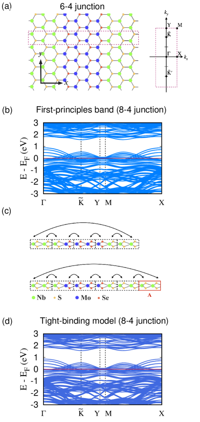
In what follows, these periodic junctions are characterized by the number of transition metal atoms in the unit cell, e.g., the - hetero-junction indicates the numbers of Nb and Mo(W) atoms to be and , respectively, in the unit cell. In this paper, the zig-zag boundary structure is adopted because the experimentally observed interface is in this structure.Gong et al. (2014); Duan et al. (2014); Huang et al. (2014); Chen et al. (2015a, b); Li et al. (2015); Zhang et al. (2015); He et al. (2016); Najmzadeh et al. (2016) In the calculations, the lattice structure is assumed to be commensurate with a unique lattice constant, Å for NbS2-MoSe2 (Å for NbS2-WSe2), which provides the minimal total energy of electronic system according to the numerical results in Fig. 2.
In Fig. 4(b), the electronic band structure of an 8-4 periodic hetero-junction is presented as an example. There is an energy gap from 1.0 eV to 1.8eV in the band structure. The subbands below the gap are attributed to the valence band of MoSe2 and the partial filled band of NbS2. The band structure possesses two local maxima between the and points. The local maximum at the point is attributed to that of the valley in the pristine TMDCs and the other local maximum at the corresponds to the valley. Thus, the electronic structure implies that the valley degree of freedom is preserved even in the hetero-junction.
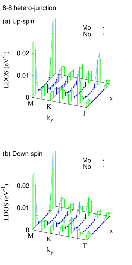
The theoretical model also reveals accumulation of charge-transfer between the metallic and semiconducting regions in the and valleys. The local electronic structure in the junction is investigated by using a tight-binding model for the periodic junction where the unit cell is shown in Fig. 4(a). In the tight-binding model, the basis consists of all outer -orbitals in transition-metal atoms and -orbitals in chalcogen atoms within the unit cell. The hopping integrals are calculated by using wannier90, Mostofi et al. (2008) a code to compute the maximally-localized Wannier orbitals and the hopping matrices between them from a first-principles band structure. For investigating the local structure, the local density of states (LDOS) is evaluated at the atomic position of Mo and Nb atoms for several , where the LDOS is represented by
| (1) |
with the band index , the orbital index in a transition-metal atom at , and the spin index along the -axis. Here, and are the eigen energy and eigenvector, respectively, of the electronic state with in the -th band. Since electronic states near the Fermi level are mainly consisting of the -orbitals in transition-metal atoms, the LDOS represents the connectivity of the electronic wave around the junction in the Fermi level.
The numerical results of LDOS in a hetero-junction is presented for the up- and down-spin states in Fig. 5 where , , and represent corresponding to , , and points, respectively, in the pristine crystal. The amplitude in the NbS2 region is much larger than that in the MoSe2 region. This observation shows that the two regions of MoSe2 and NbS2 maintain the electronic properties of semiconductor and metal, respectively. In the MoSe2 region, the LDOS is enhanced for up-spin states around the point. The enhancement is attributed to the charge transfer from the metallic region to the semiconducting region in the valley, where the valence top appears in the pristine monolayer. Since the electronic structure of the down-spin electron is mirror symmetric in , the down-spin electrons transfer in the valley. Therefore, electronic states are connected around the and points with up-spin and down-spin, respectively, in the Fermi energy through the semiconducting region.
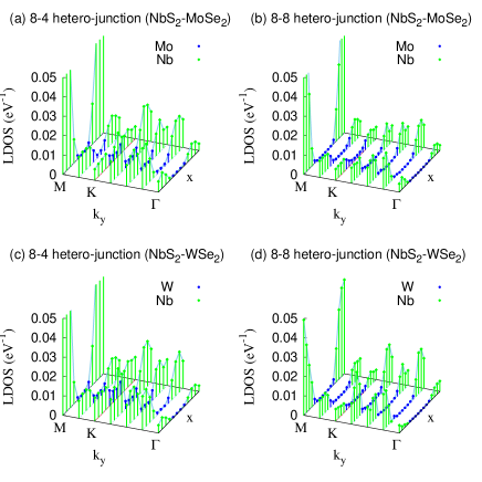
The LDOS varies with the atomic species and the length of semiconducting region as shown in Fig. 6. The numerical results show that the LDOS decreases with increase in the semiconducting region and it is enhanced within WSe2. On the other hand, it remains to be suppressed at the and points regardless of the length of the semiconducting region. The spatial profile of the LDOS indicates that the hetero-junction restricts the electronic transmission to the and valleys.
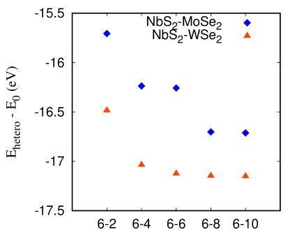
Finally, the stability of the hetero-structure is also numerically confirmed by the first-principles calculations. In Fig. 7, the energy difference by forming the junction from the independent flakes of NbS2 and MoSe2 (WSe2) is presented for several 6- hetero-junctions. Since, in every - junction, the total energy drops due to formation of the hetero-structure, the hetero-structure can remain stable. The stability of the hetero-junction does not change with the length of the NbS2 region. The energy difference is enhanced with the length of the semiconducting TMDC and saturates in the 6-10 junction. The saturation indicates that the energy change due to the addition of MoSe2 cells to the long junction is same as that to the pristine MoSe2. This implies that the local electronic structure in the middle area of the MoSe2 region is similar to that of pristine MoSe2.
III.2 Tight-binding description for hetero-junctions
A tight-binding model is constructed for the investigation of electronic transport in hetero-junctions by using hopping matrices for the periodic junction and the pristine crystal. A hetero-junction is divided into three domains: two leads and an intermediate region including two boundaries. The electronic states in the leads of NbS2 are described by using the hopping matrices for the pristine crystal.
In the intermediate region, the tight-binding Hamiltonian for the periodic junction is applied to the description. The unit cell is containing two transition-metal atoms and four chalcogen atoms as shown in Fig. 4(c) where it is reconstructed by dividing up that of periodic junctions shown in Fig. 4(a). The tight-binding model is represented by
| (2) |
where the index denotes the position of the cell, and and are the intra- and nearest-neighbor inter-cell hopping matrices, respectively. The two cells on the both side of the center of the NbS2 region are adopted as and . Here, is a state vector which consists of the annihilation operators in the spinful Wannier orbitals within the -th cell, where there are ten -orbitals in transition-metal atoms and twelve -orbitals in chalcogen atoms for each spin. In the periodic junction, the periodic boundary condition is given by substituting with .
The tight-binding Hamiltonian for the infinitely long hetero-junction is represented by
| (3) |
where the hopping matrices for the periodic junction are applied to those in . The two cells with and are connected to the edges of two leads of NbS2 with the hopping matrix for the pristine NbS2. The hopping matrices for the pristine NbS2 are also applied to those in the cells for and . For the smooth connection between the intermediate and lead regions, hopping matrices at the edges of intermediate region should be similar to those in the leads.
By adopting a long NbS2 region, the local electronic structure in the NbS2 region of the periodic junction can be similar to that in the pristine crystal. For example, a nearest-neighbor tight binding model for an 8-4 periodic hetero structure is constructed by using hopping integrals computed from the band structures of a 6-4 periodic hetero-structure and pristine monolayer NbS2. The procedure is schematically depicted in Fig. 4(c). The upper panel represents the schematic of a tight-binding model for the 6-4 periodic hetero-structure. To construct the 8-4 model, a hopping matrix from the pristine NbS2 is introduced in the cell A, the middle block in the NbS2 region, as shown in the lower panel. The inter-cell hopping from/to the cell A is that for the 6-4 periodic hetero-structure. In Fig. 4(d), the band structure of the 8-4 hetero-junction calculated by using this tight-binding model is presented and it is almost same as that from first-principles calculation in Fig. 4(b). The similarity of the two band structures shows that the electronic structure in the NbS2 region apart from the vicinity of the interface is almost same as those in the pristine crystal and that the model can well describe electronic states in the 8-4 hetero junction. Therefore, the hopping matrices of the 6- periodic junction are applied to those in intermediate region of infinitely long hetero junctions.
IV Electronic transport property of metal-semiconductor-metal junction
In this section, the electronic transport properties of a metal-semiconductor-metal lateral hetero junction are theoretically investigated within a two-terminal system. The transmission probability in the hetero-junction is calculated by using the lattice Green’s function method. The theoretical calculation shows that the hetero-junction restricts the spin of transmittable electrons in each valley in the presence of a long semiconducting region. The I-V characteristic is obtained by the Landaurer formula with the transmission probability.
IV.1 Calculation method
The electric current is calculated by the Landauer formula,
| (4) |
with a source-drain bias , where and represent the velocity along the direction and the distribution function, respectively. Here, represents the transmission probability from the incoming state to the outgoing state in the left and right half-infinite NbS2 regions, respectively. Since electrons are scattered in a short intermediate region, the dissipation of electronic energy is ignored i.e., in the scattering process. The atomically-aligned interface preserves the wave number in the direction. Therefore, the Landauer formula can be rewritten by using the conductivity for the electronic energy ,
| (5) |
with
| (6) |
where the definition of velocity is used. Here, the subscripts and are the indexes to indicate the incoming and outgoing channels in the energy at the wave number .
The transmission probability is computed by using the Green’s function method with the multi-orbital tight-binding model.Ando (1991); Habe and Koshino (2015, 2016) The Green’s function describes electronic transfer from an incoming state to an outgoing state in the leads. The wave function in leads is translational symmetric and represented by
| (7) |
where and are the intra- and inter-cell hopping matrix in the pristine NbS2. The wave functions are classified into the right-going states, which have a positive velocity or , and the left-going states, which have a negative velocity or . The Green’s function for the junction is obtained by using the self-energy in leads,
| (8) |
with
| (9) |
where is omitted from the representation for simplicity. Here, two diagonal matrices and are introduced, where and are the eigenvalue and the eigenvector for right(left)-going states, respectively, with the number of Wannier orbitals in the unit cell. The Green’s function for incoming electrons from the left-lead is calculated by the following procedure,
| (10) |
with for and the connection to the right-lead is given by
| (11) |
The transmission probability is represented by
| (12) |
where and are the indexes of incoming and outgoing channels, respectively, and it is calculated for each .
IV.2 Numerical results
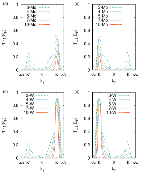
Firstly, the wave number, of the incident electronic wave, dependence of electronic transmission probability is investigated in the Fermi energy. In Fig. 8, the transmission probability is presented for several lengths of the semiconducting region. Here, is the mean probability of all incident electrons with the spin and . Up-spin and down-spin electrons show the inverted profiles in the -axis because of the mirror symmetric lattice structure. The numerical results show electrons can transmit through the junction with high probabilities around the and points. Especially in the long semiconducting regions, the electronic transmission in the () valley is permitted for up-spin (down-spin) electrons. In the () valley, on the other hand, the transmission probability for up-spin (down-spin) electrons rapidly decreases to zero with the length of the semiconducting region. These observations show that the long hetero-junction enables us to produce the spin-valley locking for conducting electrons in the metallic TMDC without any exterior equipment, e.g., gate electrode or magnetic substrate, as shown in Fig. 1(a). Moreover, WSe2 provides a high transmission probability over 0.8 compared with MoSe2 even in the junction with the longest semiconducting region.
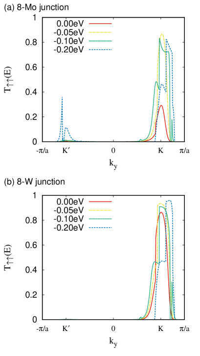
The hetero-junction also provides the spin-valley locking for electrons with various energies through a long semiconducting region. In Fig. 9, the mean transmission probability for up-spin is presented for several energies in the hetero-junction with a long semiconducting region, where the probability for down-spin shows the inverted profile in the -axis. The numerical calculations for are omitted because the electronic transmission is strongly suppressed due to the reduction of the LDOS in the semiconducting region. Large transmission probabilities are observed only around the under all conditions. Especially in the hetero-junction of MoSe2, the decrease in enhances the transmission probability. However, the transmission through MoSe2 is also recovered in the valley for eV even with the long semiconducting region. These observations indicate the stability of the novel function to provide the spin-valley locking in the hetero-junction.
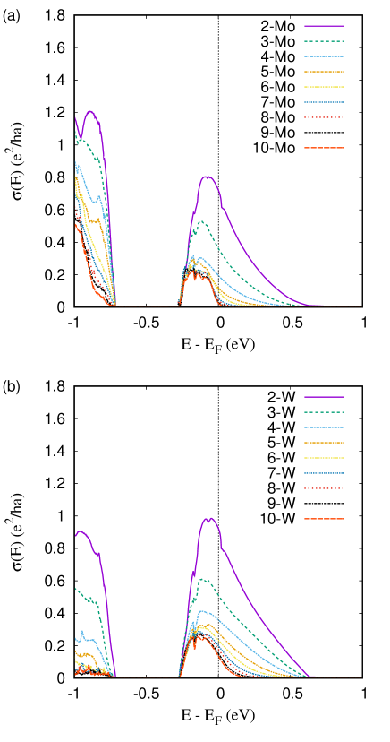
The electric conductivity of the hetero-junction shows characteristic features corresponding to the electronic structure. The energy dependence of electric conductivity is presented for several hetero-junctions of MoSe2 and WSe2 in Fig. 10, and the I-V characteristic is shown in Fig. 1(b). The conductivity increases with decreasing the length of the semiconducting region in the whole energy region. This observation indicates the increase of transmission probability with shortening MoSe2 or WSe2 regardless of energy and consistent with the variation of LDOS. In both cases of MoSe2 and WSe2, there is an insulating energy region independent of the length of intermediate region and the atomic species between eV and eV. This insulating region corresponds to the flat I-V characteristic in the and the energy gap between the partially filled band and the lower band of monolayer NbS2 as shown in Fig. 3(a). Since this energy gap is present in NbS2 and absent in NbSe2Habe (2020), the insulating energy region, the flat I-V characteristic, is a unique property of NbS2 lead. The electronic transmission in the another insulating energy region in is attributed to the electronic properties of the intermediate region of MoSe2 or WSe2. In the pristine semiconducting TMDCs, there is no conducting channel above the Fermi energy. The small conductivity for is attributed to the small LDOS due to the charge transfer from the metallic region.
The I-V characteristics of metal-semiconductor-metal lateral hetero junctions show that the junction possesses an applicable electronic property in classical electronics. In all conditions of the intermediate region, the step-like behavior is observed as a function of the bias voltage and the step height strongly depends on the length of the intermediate region. The electric current, the step height, increases with decreasing the length but the variation is different between the positive and negative voltage regions. In the region, the non-zero flow remains in junctions with long intermediate lattices of semiconducting TMDCs. The electric current in the region, on the other hand, decreases to zero with the length. The numerical results show that the rectification effect can be obtained within a monolayer hetero-junction by using a long intermediate region. The variation of the I-V characteristic is attributed to the variation of electric conductivity in the two energy regions.
V Discussion
In this section, the discussion about the relation between the electronic transport phenomena and the electronic structure is provided. Moreover, a possible effect of spin-valley locking on the electronic transport phenomena is discussed. The numerical calculations show that the NbS2-MoSe2-NbS2 and NbS2-WSe2-NbS2 hetero junctions produce the spin-valley locking for conducting electrons. This phenomenon is attributed to the different spin and momentum dependencies of transmission probability. The conducting channels in the NbS2 region are distributed in three valleys, , K, and K’, but they link to another metallic region only in the K and K’ valleys through the semiconducting region. The connection of conducting channels can be observed as non-zero LDOS in Fig. 6 and also strongly depends on the electronic spin. This behaviour indicates that the charge transfer occurs in the valley for up-spin electrons and the valley for down-spin electrons. In the semiconducting -TMDCs, the highest energy occupied states appear at the and points in the valence band and they possess the up-spin and the down-spin at the and points, respectively, due to the Zeeman-type spin-orbit coupling. Therefore, electrons in high energy states transfer to the NbS2 region and produce the spin-polarized conducting channels around the and points in the semiconducting region.
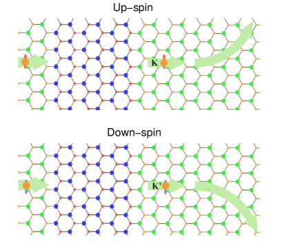
The spin-valley locking provides the enhancement of electronic transport phenomena related to the Berry curvature. The electronic states in NbS2 retain a similar structure of Berry curvature to that in semiconducting TMDCs, e.g., MoS2.Habe (2020) In the and valleys, the Berry curvature increases in intensity and possesses the opposite sign, and it shows the threefold symmetric sign change with a small amplitude in the valley. Since the spin of the transmitted electron is polarized upward in the valley and downward in the valley, the up-spin and down-spin electrons obtain the opposite velocity in the -direction attributed to the Berry curvature as shown in Fig. 11. Moreover, conducting electrons in the valley, which are less affected by the Berry curvature, are omitted from electronic transport phenomena. Thus, for example, the hetero-junction can provide an intrinsic spin Hall system with a pure spin Hall current, which consists of the opposite flows of up-spin and down-spin electrons. In the pristine metallic -TMDCs, on the other hand, each electronic spin possesses conducting channels in the , K, and K’ valleys, and it obtains different velocities in the three valleys corresponding to the sign of Berry curvature. Therefore, the semiconducting region of a hetero-junction can drastically enhance the spin Hall effect in the metallic TMDC.
VI Conclusion
In this paper, we theoretically investigated the electronic transport properties of metal-semiconductor-metal lateral-hetero junctions of -TMDCs, and revealed that the semiconducting region enables us to produce the spin-valley locking for conducting electrons in the and valleys, and omits electrons in the valley from the electronic transport phenomena. By using first-principles calculations, we show the stability of the hetero-junction consisting of NbS2 and Se2 for =W or Mo. Moreover, the numerical calculations show that the charge transfer occurs between the metallic region and the semiconducting region only in the and valleys, and it produces conducting channels in these valleys. The long semiconducting region permits the non-zero LDOS for up-spin and down-spin electrons in the and valleys, respectively. The electronic transport properties of the hetero-junction were investigated by using the lattice Green’s function method with a multi-orbital tight-binding model obtained from first-principles bands. The theoretical calculations show that the electronic transmission probability strongly depends on the spin and the wave number. Especially in long semiconducting regions, up-spin and down-spin electrons can transmit only in the and valleys, respectively. Therefore, the hetero-structure produces a novel electronic system possessing conducting electrons with the intrinsic spin-valley locking. Moreover, it is shown that the hetero-junctions are atomically thin materials with a fundamental electronic property, the step-like I-V characteristic, in classical electronics.
References
- Lee et al. (2012) Y.-H. Lee, X.-Q. Zhang, W. Zhang, M.-T. Chang, C.-T. Lin, K.-D. Chang, Y.-C. Yu, J. T.-W. Wang, C.-S. Chang, L.-J. Li, and T.-W. Lin, Adv. Mater. 24, 2320 (2012).
- Bergeron et al. (2017) H. Bergeron, V. K. Sangwan, J. J. McMorrow, G. P. Campbell, I. Balla, X. Liu, M. J. Bedzyk, T. J. Marks, and M. C. Hersam, Applied Physics Letters 110, 053101 (2017).
- Chen et al. (2017) K.-C. Chen, T.-W. Chu, C.-R. Wu, S.-C. Lee, and S.-Y. Lin, Journal of Physics D: Applied Physics 50, 064001 (2017).
- Moreau et al. (2010) E. Moreau, S. Godey, F. J. Ferrer, D. Vignaud, X. Wallart, J. Avila, M. C. Asensio, F. Bournel, and J.-J. Gallet, Applied Physics Letters 97, 241907 (2010).
- Zhan et al. (2017) L. Zhan, W. Wan, Z. Zhu, T.-M. Shih, and W. Cai, Journal of Physics: Conference Series 864, 012037 (2017).
- El Kazzi et al. (2018) S. El Kazzi, W. Mortelmans, T. Nuytten, J. Meersschaut, P. Carolan, L. Landeloos, T. Conard, I. Radu, M. Heyns, and C. Merckling, Journal of Applied Physics 123, 135702 (2018).
- Castro Neto et al. (2009) A. H. Castro Neto, F. Guinea, N. M. R. Peres, K. S. Novoselov, and A. K. Geim, Rev. Mod. Phys. 81, 109 (2009).
- Xiao et al. (2012) D. Xiao, G.-B. Liu, W. Feng, X. Xu, and W. Yao, Phys. Rev. Lett. 108, 196802 (2012).
- Kang et al. (2013) J. Kang, S. Tongay, J. Zhou, J. Li, and J. Wu, Applied Physics Letters 102, 012111 (2013).
- Habe and Koshino (2015) T. Habe and M. Koshino, Phys. Rev. B 91, 201407(R) (2015).
- Li et al. (2015) M.-Y. Li, Y. Shi, C.-C. Cheng, L.-S. Lu, Y.-C. Lin, H.-L. Tang, M.-L. Tsai, C.-W. Chu, K.-H. Wei, J.-H. He, W.-H. Chang, K. Suenaga, and L.-J. Li, Science 349, 524 (2015).
- Najmzadeh et al. (2016) M. Najmzadeh, C. Ko, K. Wu, S. Tongay, and J. Wu, Applied Physics Express 9, 055201 (2016).
- Son et al. (2016) Y. Son, M.-Y. Li, C.-C. Cheng, K.-H. Wei, P. Liu, Q. H. Wang, L.-J. Li, and M. S. Strano, Nano Letters 16, 3571 (2016).
- Ullah et al. (2017) F. Ullah, Y. Sim, C. T. Le, M.-J. Seong, J. I. Jang, S. H. Rhim, B. C. Tran Khac, K.-H. Chung, K. Park, Y. Lee, K. Kim, H. Y. Jeong, and Y. S. Kim, ACS Nano 11, 8822 (2017).
- Mak et al. (2010) K. F. Mak, C. Lee, J. Hone, J. Shan, and T. F. Heinz, Phys. Rev. Lett. 105, 136805 (2010).
- Jin et al. (2013) W. Jin, P.-C. Yeh, N. Zaki, D. Zhang, J. T. Sadowski, A. Al-Mahboob, A. M. van der Zande, D. A. Chenet, J. I. Dadap, I. P. Herman, P. Sutter, J. Hone, and R. M. Osgood, Phys. Rev. Lett. 111, 106801 (2013).
- Zhang et al. (2014) Y. Zhang, T.-R. Chang, B. Zhou, Y.-T. Cui, H. Yan, Z. Liu, F. Schmitt, J. Lee, R. Moore, Y. Chen, H. Lin, H.-T. Jeng, S.-K. Mo, Z. Hussain, A. Bansil, and Z.-X. Shen, Nat. Nano. 9, 111 (2014).
- Lu et al. (2015) J. M. Lu, O. Zheliuk, I. Leermakers, N. F. Q. Yuan, U. Zeitler, K. T. Law, and J. T. Ye, Science 350, 1353 (2015).
- Xi et al. (2015) X. Xi, Z. Wang, W. Zhao, J.-H. Park, K. T. Law, H. Berger, L. Forro, J. Shan, and K. F. Mak, Nature Physics 12, 139 (2015).
- Xi et al. (2016) X. Xi, H. Berger, L. Forró, J. Shan, and K. F. Mak, Phys. Rev. Lett. 117, 106801 (2016).
- Wang et al. (2017) H. Wang, X. Huang, J. Lin, J. Cui, Y. Chen, C. Zhu, F. Liu, Q. Zeng, J. Zhou, P. Yu, X. Wang, H. He, S. H. Tsang, W. Gao, K. Suenaga, F. Ma, C. Yang, L. Lu, T. Yu, E. H. T. Teo, G. Liu, and Z. Liu, Nature Communications 8, 394 (2017).
- Habe (2019a) T. Habe, Phys. Rev. B 100, 165431 (2019a).
- Lu et al. (2016) S.-C. Lu, M. Mohamed, and W. Zhu, 2D Materials 3, 011010 (2016).
- Sharma et al. (2014) M. Sharma, A. Kumar, P. K. Ahluwalia, and R. Pandey, Journal of Applied Physics 116, 063711 (2014).
- Habe (2019b) T. Habe, Journal of Applied Physics 126, 123901 (2019b).
- Deilmann et al. (2020) T. Deilmann, M. Rohlfing, and U. Wurstbauer, Journal of Physics: Condensed Matter 32, 333002 (2020).
- Gong et al. (2014) Y. Gong, J. Lin, X. Wang, G. Shi, S. Lei, Z. Lin, X. Zou, G. Ye, R. Vajtai, B. I. Yakobson, H. Terrones, M. Terrones, B. Tay, J. Lou, S. T. Pantelides, Z. Liu, W. Zhou, and P. M. Ajayan, Nature Materials 13, 1135 (2014).
- Duan et al. (2014) X. Duan, C. Wang, J. C. Shaw, R. Cheng, Y. Chen, H. Li, X. Wu, Y. Tang, Q. Zhang, A. Pan, J. Jiang, R. Yu, Y. Huang, and X. Duan, Nature Nanotechnology 9, 1024 (2014).
- Huang et al. (2014) C. Huang, S. Wu, A. M. Sanchez, J. J. P. Peters, R. Beanland, J. S. Ross, P. Rivera, W. Yao, D. H. Cobden, and X. Xu, Nature Materials 13, 1096 (2014).
- Chen et al. (2015a) K. Chen, X. Wan, W. Xie, J. Wen, Z. Kang, X. Zeng, H. Chen, and J. Xu, Advanced Materials 27, 6431 (2015a).
- Chen et al. (2015b) K. Chen, X. Wan, J. Wen, W. Xie, Z. Kang, X. Zeng, H. Chen, and J.-B. Xu, ACS Nano 9, 9868 (2015b).
- Zhang et al. (2015) X.-Q. Zhang, C.-H. Lin, Y.-W. Tseng, K.-H. Huang, and Y.-H. Lee, Nano Letters 15, 410 (2015).
- He et al. (2016) Y. He, A. Sobhani, S. Lei, Z. Zhang, Y. Gong, Z. Jin, W. Zhou, Y. Yang, Y. Zhang, X. Wang, B. Yakobson, R. Vajtai, N. J. Halas, B. Li, E. Xie, and P. Ajayan, Advanced Materials 28, 5126 (2016).
- Giannozzi et al. (2009) P. Giannozzi, S. Baroni, N. Bonini, M. Calandra, R. Car, C. Cavazzoni, D. Ceresoli, G. L. Chiarotti, M. Cococcioni, I. Dabo, A. Dal Corso, S. de Gironcoli, S. Fabris, G. Fratesi, R. Gebauer, U. Gerstmann, C. Gougoussis, A. Kokalj, M. Lazzeri, L. Martin-Samos, N. Marzari, F. Mauri, R. Mazzarello, S. Paolini, A. Pasquarello, L. Paulatto, C. Sbraccia, S. Scandolo, G. Sclauzero, A. P. Seitsonen, A. Smogunov, P. Umari, and R. M. Wentzcovitch, J. Phys.: Condens. Matter 21, 395502 (2009).
- Mostofi et al. (2008) A. A. Mostofi, J. R. Yates, Y.-S. Lee, I. Souza, D. Vanderbilt, and N. Marzari, Computer Physics Communications 178, 685 (2008).
- Ando (1991) T. Ando, Phys. Rev. B 44, 8017 (1991).
- Habe and Koshino (2016) T. Habe and M. Koshino, Phys. Rev. B 93, 075415 (2016).
- Habe (2020) T. Habe, Phys. Rev. B 102, 195430 (2020).