Direct observation of discommensurate charge density wave modulation in the quasi-1D Weyl semimetal candidate NbTe4
Abstract
The transition-metal tetrachalcogenides are a model system to explore the conjunction of correlated electronic states such as charge density waves (CDW), with topological phases of matter. Understanding the connection between these phases requires a thorough understanding of the individual states, which for the case of the CDW in this system, is still missing. In this paper we combine phonon-structure calculations and scanning tunneling microscopy measurements of NbTe4 in order to provide a full characterization of the CDW state. We find that, at short range, the superstructure formed by the CDW is fully commensurate with the lattice parameters. Moreover, our data reveals the presence of phase-slip domain-walls separating regions of commensurate-CDW in the nanoscale, indicating that the CDW in this compound is discommensurate at long-range. Our results solve a long-standing discussion about the nature of the CDW in these materials, and provide a strong basis for the study of the interplay between this state and other novel quantum electronic states.
Introduction
Transition-metal chalcogenides are a model family to study a large variety of quantum phenomena including charge density wave (CDW) formation, superconductivity, topological states and magnetism Manzeli et al. (2017); Monceau (2012); de Lima et al. (2019). Among this family, the quasi-1-dimensional transition-metal tetrachalcogenides, with their representative members: NbTe4 and TaTe4, have recently gained a renewed interest due to the possibility of hosting axionic states connecting different Weyl-points in the Fermi-surface through the formation of a CDW Zhang et al. (2020); Gooth et al. (2019); Sun et al. (2020); Zhang et al. (2020). Therefore these compounds provide an ideal opportunity to study the connection between topological states of matter and correlated electronic states such as CDWs Boswell et al. (1983); Walker (1985). In addition, recent high-pressure experiments have reported the presence of superconductivity in both, NbTe4 Yang et al. (2018) and TaTe4 Yuan et al. (2020), making them strong candidates for a new class of topological superconductors. All of these novel phenomena motivate a thorough characterization of the different physical properties of these materials, in particular, of the details and origin of the CDW at low-temperatures, where the possible topological properties are more likely to be observed.
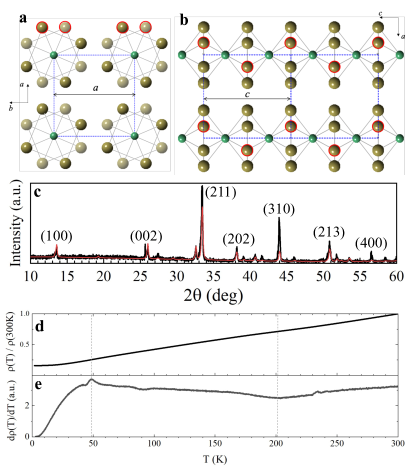
The crystal structure of NbTe4 originates from subtle deformations of its high-temperature tetragonal space group P4/mcc, shown in figure 1(a,b), with reported unit cell parameters =6.499 Å and =6.837 Å at room-temperature, and confirmed by our x-ray data (fig. 1c) Selte and Kjekshus (1964). In this structure, Nb-atoms are at the center of two square antiprisms of Te-atoms, each rotated with respect to the other (fig. 1a). These units form linear chains in the c-direction (fig. 1b), which are bonded to other chains by van der Waals interactions. As a consequence, single crystals of this compound grow as long-needles parallel to the c-axis, which evidences the quasi-one-dimensional character of its crystal structure.
X-ray and electron diffraction studies in NbTe4 have revealed distortions from the P4/mcc structure, and have associated those to several possible CDW distortions Walker and Morelli (1988); Boswell et al. (1983); Prodan and Boswell (1987). A variety of satellite peaks and streaks in the diffraction patterns develop at different temperatures and the appearance of such features roughly coincide with features observed in electrical resistivity measurements (see vertical-dashed-lines in fig. 1(d,e) for some of such features) Tadaki et al. (1990). At room-temperature, satellite peaks at , , , where and are the inverse of and , respectively, and (following the notation of Eaglesham et al.) are observed by selected-area diffraction patterns as reported by several authors Eaglesham et al. (1985); Boswell and Prodan (1986); Prodan and Boswell (1987). Below approximately 210 K to 180 K (varies for different authors and on cooling/warming history), diffuse streaks at different positions of the reciprocal space are progressively developed, and are even reported to evolve into regularly spaced spots as temperature is decreased Prodan and Boswell (1987). Below about 50 K, the different satellite diffraction peaks become commensurate with the P4/mcc lattice parameters (meaning, ), and the and peaks merge into one (). This has been interpreted as a lock-in (incommensurate-to-commensurate) transition of the CDW distortion Eaglesham et al. (1985).
Although the characterization of the lattice distortion and reciprocal space mapping of NbTe4 by diffraction experiments has been extensive, direct observation of the CDW modulation by real-space imaging techniques is scarce. Previous scanning tunnelling microscopy (STM) data attempted to characterize the charge modulation at room-temperature, however, with a limited resolution Prodan et al. (1998). To our knowledge, there are no previous reports of the observation of the low-temperature CDW modulation of NbTe4 by STM experiments. Recent experiment in the other family member of the tetrachalcogenides, TaTe4, reported on the observation of a new type of charge modulation, distinct from the ones reported by diffraction experiments, presumably coming from surface effects in this compound Sun et al. (2020). All of these observations motivate a thorough characterization of the low-temperature CDW states in NbTe4 by direct imaging and spectroscopic techniques.
In this article we report on a combination of low-temperature STM measurements and phonon dispersion calculations of the quasi-1D transition-metal tetrachalcogenide NbTe4. Our measurements of the low-temperature charge distribution in the plane directly reveal, for the first time, the superstructure created by the CDW in this material, which agrees with our theory predictions. Furthermore, we present evidence for the presence of a discommensurate-CDW (i.e., commensurate regions separated by phase-slip domain-walls) at low-temperature, with wavevector and phase-slip conditions consistent with the features reported by previous diffraction experiments at room-temperature, although our measurements are performed at 1.7 K. This observation suggests that the CDW in this compound is discommensurate for all temperatures below room-temperature, therefore inviting to revisit the characteristics and conditions of the presumable lock-in transition and other intermediate-temperature transitions reported for this material. Our results provide strong evidence to solve a long-standing discussion around the characteristics of the CDW in this material, and provides a strong basis for the study of the interplay between this state and other novel quantum electronic states, such as the recently predicted Weyl-points.
Methods
.1 Computational Approach
The density functional theory, DFT Hohenberg and Kohn (1964); Kohn and Sham (1965), calculations were performed with the abinit package (v8.11.8) Gonze et al. (2009); Gonze and et al. (2020). The norm-conserving pseudopotentials from the PseudoDojo project (v0.4) van Setten et al. (2018) were used with the generalized gradient approximation PBEsol exchange correlation functional Perdew et al. (2008) and a Fermi-Dirac electronic smearing of 0.001 Hartree (Ha). The phonon calculations were performed using the density functional perturbation theory (DFPT) Gonze and Lee (1997) and a good convergence (about 1 cm-1 on the frequencies) was obtained with a -points mesh of in the reciprocal space and a cutoff energy for the plane wave expansion of 35 Ha. The phonon dispersions were interpolated with a grid of -points in the reciprocal space. The symmetry adapted mode contributions to the phase-transition was analyzed using the AMPLIMODE software Orobengoa et al. (2009).
.2 Experimental Methods
Single crystals of NbTe4 were grown using a self-flux technique Fisher et al. (2012). A mixture of 1 mol% of elemental Nb and 99 mol% of elemental Te were put in alumina crucibles and sealed in evacuated quartz tubes. The mix was heated to 700∘C, held at this temperature for 12 hours and then slowly cooled to 500∘C at a rate of 2∘C/hour. The remaining melt was decanted and separated from the NbTe4 crystals using a centrifuge. Silver-colored long rectangular prism shaped crystals were obtained, with sizes up to 0.1 0.1 1 cm3.
Powder X-ray diffraction measurements were taken from a collection of ground single crystals, in Eulerian-Cradle geometry, using a Panalytical X-Pert system. Resistivity measurements as a function of temperature (Fig. 1d,e) were taken in cleaved crystals using a four probe configuration, with electrical current running along the c-direction. Electrical contact was made using sputtered gold pads. A 4He VTI-cryostat was used to vary temperature from room-temperature down to 2 K.
STM was performed with a hybrid UNISOKU-USM1300 system constructed with a homemade ultrahigh-vacuum sample preparation and manipulation system. The samples were cleaved at room-temperature at pressures lower than torr and immediately transferred to the low temperature STM. Crystals cleave exposing the {010} surface, this is, the a-c plane. Topography was performed at 1.7 K, with typical tunneling parameters of =50–100 mV and =100–300 pA.
Results and discussion
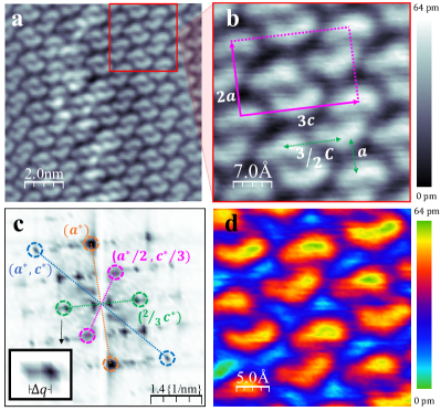
Figure 2 shows STM measurements taken at the {010} surface of a NbTe4 crystal. The cleaved-surface that is observed in the image is formed by Te-atoms in the a-c plane, as the bonding between Te-atoms is weaker than between Nb and Te Selte and Kjekshus (1964), a common feature in all low-dimensional transition-metal chalcogenides. The Te-atoms expected to be observed in the surface are highlighted in red-circles in Fig. 1b, forming zig-zag chains that run along the c-direction. The large-scale topographic image (figure 2a) reveals a periodic modulation of the electronic density, formed by rows of cashew-shaped units with alternating up-down curvatures, and with adjacent rows shifted 1/3 of a row period. This modulation forms a superstructure with unit cell as highlighted by the pink-rectangle in the close-up look to the topographic image, shown in fig. 2b. The spatial periodicity can be accurately determined through the fast Fourier transform (FFT) in Fig. 2c, resulting in a periodicity (FFT peaks labeled as ). The size of this superstructure matches the commensurate-CDW superstructure reported by several diffraction experiments at low-temperatures (50 K) Boswell et al. (1983); Eaglesham et al. (1985); Boswell and Prodan (1986). We will later discuss other important features of the FFT of the topographic image.
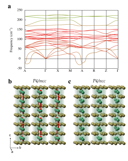
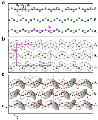
In order to explain the superstructure shown by the topography images and the origin of the CDW modulation in NbTe4, we have computed the vibrational landscape of the high-symmetry structure P4/mcc (space group (SG) 124). Fig. 3a shows the calculated phonon-dispersion curves of the P4/mcc high-symmetry structure. An instability appears at the (,,) high-symmetry point of the Brillouin zone (with the irreducible representation – irrep – ), which disperses quickly when going away from the point. However, the strongest unstable phonon frequency is located in a point between the and point, in a region close to =(,,) (irrep ). To resolve the lowest energy structure, we condensed the and unstable mode eigenvectors into two different structures, with 222 and 223 supercells with respect to the high-symmetry unit cell, respectively. We find that the phase formed by the mode (which leads to the P4/ncc - SG 130) has a lower energy than the phase formed by the mode (I4 - SG 79). This result is in good agreement with the observed 23 superstructure seen at low-temperatures in our STM data. Interestingly, our calculations show that the -mode is strongly driven by the Nb-sites with a small deviation, from the high-symmetry position, of the Te-sites. Fig. 3b shows the undistorted P4/mcc phase in which the most significant atomic displacements of the -mode are depicted by red-arrows. Once these distortions are condensed and the structure fully relaxed, the obtained structural modulation can be observed in Fig. 3c. In such a phase, the modulation induces a trimerization of the Nb-sites in the 1D-chains. The three NbNb distances, , are 3.137 Å, 3.168 Å and 3.971 Å, hence, two short and one long. This result is in line with suggestions from previous works Walker and Morelli (1988); Guster et al. (2021). Fig. 4a shows the spatial configuration of the Nb-trimers that lie just underneath a cleaved-surface, in the final modulated structure, as calculated by our DFT model. This figure highlights the A-B-A stacking of the trimers in adjacent chains, with the B-chain trimers shifted by one Nb-atom to the right (or two Nb-atoms to the left), or equivalently, to the right (or to the left), with respect to the A-chain trimers. This specific A-B-A stacking of the chains is responsible for the periodicity of the superstructure along the direction perpendicular to the chains.
The trimerization of Nb-atoms, predicted by our DFT calculations, has important consequences for the charge distribution in the cleaved-surface of the NbTe4 crystals. As mentioned previously, this surface is formed by Te-atoms. The schematic configurations shown in fig. 4a,b,c shows these surface Te-atoms in a {010} cleaved-surface, together with the Nb-atoms just underneath this surface. The cashew-shapes observed in our topographic images can be naturally explained by the trimerization of the Te-atoms in the surface, which are arranged in zig-zag along the chains, as represented in fig. 4b (see figs. A1 and A2, in Appendix, for images with atomic-resolution within a cashew). The formation of Te-trimers (or cashews) is a consequence of the trimerization of the Nb-atoms underneath. This trimerization also naturally explains the alternating up-down curvature of successive cashews within a chain. The cashew configuration along each chain, with period , is shifted by in both -up and down- adjacent chains (to the left if taken with respect to the middle-B-chain in fig. 4b, or equivalently, to the right), and in the same direction for both adjacent chains. This specific A-B-A stacking of the chains is fully equivalent to the one found in our DFT calculations, and reproduces the unit cell of the superstructure, with period , observed by our topographic images.
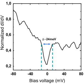
Noteworthy, the charge distribution within a single cashew-like structure is asymmetric, as is better appreciated in fig. 2d. The position where the maximum charge distribution occurs, as observed in the topography image, is shifted toward the right side on each cashew. This asymmetry is an indication that the CDW distortion indeed originates in the Nb-atoms, instead of the Te-atoms, in full agreement with our DFT calculations. Fig. 4c shows a simplified schematic representation of the Nb-atoms displacements that give rise to such an asymmetric Te-surface charge distribution. In this picture, the central Nb-atom of each Nb-trimer, where charge density is expected to be higher, is located toward the right-end of the Te-trimer, which could explain the accumulation of charge toward the right-side of the cashews in the observed Te-surface. Within this picture, the CDW is represented by the waves depicted in Fig. 4c, with a maximum amplitude right at (or very close to) the center of the Nb-trimer (which coincides with the right side of each Te-trimer or cashew), and a minimum amplitude in the space between two Nb-trimers. The wavelength of this CDW is , and it therefore implies a CDW-wavevector within each chain of . Waves in both -up and down - adjacent chains of each chain are shifted by either both to the left or both to the right, generating the observed A-B-A stacking of the superstructure. As a consequence of the CDW-wavector and the phase-shifts in adjacent chains, the observed superstructure in the Te-atoms-surface has a periodicity of , as revealed by our topographic images, and predicted by our DFT calculations. Therefore, the phonon-mode responsible for such a commensurate distortion is the -mode. The CDW-gap opened by this distortion, as determined by tunneling conductance curves, is 24 meV (see Fig. A3 in Appendix).
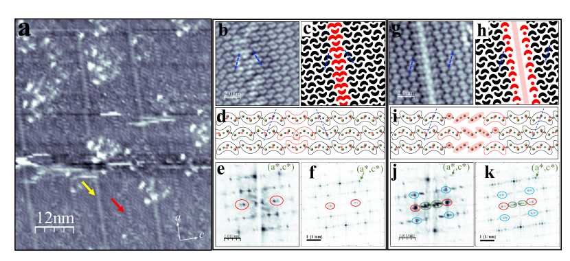
We will now discuss the intricacies of the FFT, which reveal the presence of discommesurations of the CDW in NbTe4. The FFT (fig. 2c) of the topographic image of fig. 2a reveals other intense peaks, in addition to the peaks of the superstructure unit cell. Interestingly, the peak around (highlighted in the green-circle) is split in two, as can be better observed in the inset to this figure. Although the presence of split peaks as well as the presence of other satellite peaks in diffraction experiments have been interpreted as signatures of incommensurate CDWs Boswell et al. (1983); Prodan and Boswell (1987); Prodan et al. (1990), we argue that all satellite peaks observed by diffraction experiments in all ranges of temperatures are a consequence of discommensurations of a unique commensurate CDW-phase, this is, regions of commensurate CDW separated by domain-walls. Figure 5a shows a wide-area topographic image of a cleaved NbTe4 surface. Long columnar features along the a-direction, and running from top-to-down all through the image, can be observed. An example of one of the features with the largest contrast is indicated by the yellow-arrow. However, other types of columnar features that generate less contrast in the topographic image can be observed, as for example, the one highlighted by the red-arrow. Careful and closer inspection to different areas containing such columnar features reveal different patterns. Two examples of the type of features that can be found are shown in Figs. 5b (same as in fig. 2a) and fig. 5g. The FFT of these images (figs. 5e and 5j, respectively) show marked differences. For instance, whereas the peaks (red-ovals) in fig. 5e, for the first type of domain-wall, are split, as discussed earlier, the peaks are not. In contrast, both of those set of peaks in the FFT shown in fig. 5j (red-ovals in this figure), for the second type of domain-wall, are split and, furthermore, additional peaks along the horizontal-axis, close to the origin (green-ovals), appear in this FFT. Fig. 5c shows a cartoon model of the distortion of the cashews pattern of the image in fig. 5b. The domain-wall is highlighted by the cashews in red. This type of domain-wall can be generated by the situation depicted in fig. 5d in which, within a chain, two nearest-neighbors Nb-trimers share one atom, implying a CDW phase-slip of to the left within the chain. This, for the Te-trimers at the surface, results in the partial-merge of two cashews and therefore, the vertical flip of one of them. The Nb (and Te) trimers in adjacent chains remain intact, creating a domain-wall with alternating double-simple cashews. One way to validate this picture is observing the flip in CDW phase-difference between successive chains on the left and right of the domain-wall: with respect to the top-chain in fig. 5d, the CDW-phase of the middle row is shifted to the left, on the left of the domain-wall, but to the right, on the right of the domain-wall. This is represented by the flip in orientation of the dashed-blue-lines in figs. 5(b,c,d). The FFT of the cartoon model in fig. 5c is shown in fig. 5f, and it reproduces the main features observed in the FFT of the corresponding real topographic image. The main characteristics of the second example of possible domain-walls, shown in fig. 5g, are captured by the cartoon model in fig. 5h. This pattern can be obtained by the situation shown in fig. 5i, in which five Nb-atoms within a chain are not clearly bound to trimers, deriving in a CDW phase-slip of to the right, or equivalently, to the left, within each chain. This phase-slip happens for every chain in the structure, which implies an equivalent CDW interchain phase-shift at the right and left of the domain-wall (situation highlighted by the dashed-blue-lines in figs. 5(g,h,i)), in contrast with the first example of domain-wall. The FFT of the cartoon model is shown in fig. 5k, and also reproduces the main features of the FFT of the corresponding real topographic image.
Other types of domain-walls, different from the two examples discussed previously, can be found within our topographic images. In principle, a domain-wall can be created by any possible combination of phase-slips for different chains. Nevertheless, only intrachain CDW phase-slips of (or equivalently, displacements of cashews, where is an integer) are allowed by the symmetry of the crystal structure and the CDW-wavelength, which limits the possibilities for domain-wall configurations. This constrain in the phase-slip can be the reason for the finite set of satellite peaks found in diffraction experiments. Moreover, the values for splittings reported by such diffraction experiments match the values found for splittings in the FFT peaks of our topographic images. The distance between the split peaks around the position in figs. 2c and 2e is nm, which matches the value of the splitting between satellite diffraction peaks and , i.e., , with . These values are equivalent to the ones reported by diffraction experiments by several authors Eaglesham et al. (1985); Boswell et al. (1983); Boswell and Prodan (1986); Prodan and Boswell (1987). This highly suggests that, what had been interpreted before as signatures of the presence of incommesurate CDWs in NbTe4 are, on the other hand, signatures of discommensurations due to phase-slip domain-walls, which separate regions of commensurate-CDW with wavevector within a chain, phase-difference of with adjacent chains, and ABA stacking.
An important characteristics of the domain-walls is that they run over large distances along the same line in the a-direction, with no (or minor) disruptions, and are not necessarily periodic along the c-direction. The highly coherent domain-walls along the a-direction may be a consequence of the interchain coupling strength, which for NbTe4 is much more significant than for other low-dimensional transition-metal chalcogenides. For instance, the interchain Te-Te distance in the tetrachalcogenides is shorter than the intrachain Te-Te distance, which has been predicted to result in the formation of interchain Te-Te dimers that can hybridize with the transition-metal atoms, leading to a large metallic conduction in the direction perpendicular to the chains Bullett (1984); Guster et al. (2021). In fact, the resistivity anisotropy of NbTe4 has been reported to be very close to 1 Tadaki et al. (1990), unexpected for such an anisotropic quasi-1D crystalline structure. The results presented by our study inspire relevant question that can help understanding these electronic properties. For example, the large tunnel conductance values observed in some of the domain-walls, which could be an indication of a largest charge density, invites to study the domain-walls contribution to the electronic conductance in the a-direction. On the other hand, similarly long and coherent columnar domain-walls have been observed in other low-dimensional systems (for example, graphene nanostructures Vicarelli et al. (2015)), in which topological defects due to atomic vacancies in the crystalline structure form extended dislocations. A similar mechanism could also be the origin of the observed CDW domain-walls in NbTe4, possibly originated by Te-vacancies. Another relevant question is the influence of random quenched disorder on the domain-wall density, coherence length, and even CDW fundamental properties, as observed for other prototypical CDW systems Fang et al. (2019).
It is important to emphasize that our STM measurements have been performed at low-temperature, and not at room-temperature. The presence of split peaks in diffraction experiments have been reported at room-temperature, with the appearance of other streaks and peaks as temperature is lowered. The equivalent characteristics of the FFTs of our topographic images and the ones reported by diffraction experiments suggest that the CDW in NbTe4 is discommensurate and with an unchanged CDW-wavevector from room-temperature down to 1.7 K. Nevertheless, resistivity measurements as a function of temperature (see fig. 1d,e) reveal marked changes of slope at certain temperatures (both in our data and data taken by other authors), which have been historically interpreted as CDW phase-transitions. Interestingly, a temperature of 50 K, at which a marked feature in the derivative of the vs T curve appears (see fig. 1e), seems to coincide with the temperature below which the peak splitting and presence of diffuse streaks disappear in electron diffraction experiments, which has been interpreted as a lock-in (incommensurate-to-commensurate) transition of the CDW. As argued, the features observed in diffraction experiments could be explained by discommensurations, rather than incommensurations of the CDW, inviting to consider the configuration and dynamics of the phase-slip domain-walls as possible candidates driving the presumed phase-transitions suggested by the features in resistivity curves and diffraction experiments.
Finally, it is pertinent to highlight that our topographic data can be fully reproduced by the condensed phonon-instability predicted by our DFT calculations. This indicates that an electron-phonon coupling mechanism is largely responsible for the commensurate-CDW formation in this compound, in contrast to the Fermi-surface nesting or Peierls mechanism commonly expected in low-dimensional compounds Grüner (1988). This observation is in line with previous works suggesting the electron-phonon mechanism as the dominant driving force for CDW formation in most real materials, even in the 1D limit Johannes and Mazin (2008); Guster et al. (2021). Since the transition-metal tetrachalcogenides have been predicted to host Weyl-nodes in their electronic structure, our results motivate further theoretical and experimental studies aimed at understanding the influence of electron-phonon coupling on the determination of complex Fermi-surface topologies and its connection with novel topological quasiparticles in materials Parente et al. (2013); Heid et al. (2017); Garcia et al. (2021).
Acknowledgements
The authors thanks C. A. Mera, L. Quiroga, F. Rodriguez, H. Suderow, I. Guillamon and E. Herrera for enlightening discussions. J.A.G., D.J-G., J.R-C., J.C., O.H. and P.G-G. thank the support of the Ministerio de Ciencia, Tecnología e Innovación de Colombia (Grants No. 120480863414 and No. 122585271058). P.G-G. and I.R.F. thank the support of the APS International Travel Grant Award Program which enabled P.G-G. to visit Stanford University. P.G-G. thanks the support of the L’Oréal-UNESCO For Women in Science International Rising Talents Programme, the School of Sciences and the Vice Presidency of Research and Creation at Universidad de Los Andes. J.A.G., J.C. and O.H. thank the support of Clúster de Investigación en Ciencias y Tecnologías Convergentes NBIC, Universidad Central. I.R.F., A.F. and A.K. were supported by the Department of Energy, Office of Basic Energy Sciences, under contract DE-AC02-76SF00515.
This work used the DECI PRACE project OFFSPRING and the CECI facilities funded by F.R.S-FNRS (Grant No. 2.5020.1) and Tier-1 supercomputer of the Fédération Wallonie-Bruxelles funded by the Walloon Region (Grant No. 1117545).
A.C.G.C. acknowledge the support from the GridUIS-2 experimental testbed, developed under the Universidad Industrial de Santander (SC3-UIS) High Performance and Scientific Computing Centre, with support from UIS Vicerrectoría de Investigación y Extensión (VIE-UIS) and several UIS research groups as well as other funding resources.
References
- Manzeli et al. (2017) S. Manzeli, D. Ovchinnikov, D. Pasquier, O. V. Yazyev, and A. Kis, Nature Reviews Materials 2, 17033 (2017).
- Monceau (2012) P. Monceau, Advances in Physics 61, 325 (2012), https://doi.org/10.1080/00018732.2012.719674 .
- de Lima et al. (2019) B. de Lima, N. Chaia, T. Grant, L. de Faria, J. Canova, F. de Oliveira, F. Abud, and A. Machado, Materials Chemistry and Physics 226, 95 (2019).
- Zhang et al. (2020) X. Zhang, Q. Gu, H. Sun, T. Luo, Y. Liu, Y. Chen, Z. Shao, Z. Zhang, S. Li, Y. Sun, Y. Li, X. Li, S. Xue, J. Ge, Y. Xing, R. Comin, Z. Zhu, P. Gao, B. Yan, J. Feng, M. Pan, and J. Wang, Phys. Rev. B 102, 035125 (2020).
- Gooth et al. (2019) J. Gooth, B. Bradlyn, S. Honnali, and et al., Nature 575, 315–319 (2019).
- Sun et al. (2020) H. Sun, Z. Shao, T. Luo, Q. Gu, Z. Zhang, S. Li, L. Liu, H. Gedeon, X. Zhang, Q. Bian, J. Feng, J. Wang, and M. Pan, New Journal of Physics 22, 083025 (2020).
- Boswell et al. (1983) F. W. Boswell, A. Prodan, and J. K. Brandon, Journal of Physics C: Solid State Physics 16, 1067 (1983).
- Walker (1985) M. B. Walker, Canadian Journal of Physics 63, 46 (1985), https://doi.org/10.1139/p85-007 .
- Yang et al. (2018) X. Yang, Y. Zhou, M. Wang, H. Bai, X. Chen, C. An, Y. Zhou, Q. Chen, Y. Li, Z. Wang, J. Chen, C. Cao, Y. Li, Y. Zhou, Z. Yang, and Z.-A. Xu, Scientific Reports 8, 6298 (2018).
- Yuan et al. (2020) Y. Yuan, W. Wang, Y. Zhou, X. Chen, C. Gu, C. An, Y. Zhou, B. Zhang, C. Chen, R. Zhang, and Z. Yang, Advanced Electronic Materials 6, 1901260 (2020), https://onlinelibrary.wiley.com/doi/pdf/10.1002/aelm.201901260 .
- Ikari et al. (1987) T. Ikari, H. Berger, and F. Levy, physica status solidi (b) 139 (1987), 10.1002/pssb.2221390143.
- Tadaki et al. (1990) S. Tadaki, N. Hino, T. Sambongi, K. Nomura, and F. Lévy, Synthetic Metals 38, 227 (1990).
- Selte and Kjekshus (1964) K. Selte and A. Kjekshus, Acta Chemica Scandinavica 18, 690 (1964).
- Walker and Morelli (1988) M. B. Walker and R. Morelli, Phys. Rev. B 38, 4836 (1988).
- Prodan and Boswell (1987) A. Prodan and F. W. Boswell, Acta Crystallographica Section B 43, 165 (1987).
- Eaglesham et al. (1985) D. J. Eaglesham, D. Bird, R. L. Withers, and J. W. Steeds, Journal of Physics C: Solid State Physics 18, 1 (1985).
- Boswell and Prodan (1986) F. W. Boswell and A. Prodan, Phys. Rev. B 34, 2979 (1986).
- Prodan et al. (1998) A. Prodan, S. W. Hla, V. Marinković, H. Böhm, F. W. Boswell, and J. C. Bennett, Phys. Rev. B 57, 6235 (1998).
- Hohenberg and Kohn (1964) P. Hohenberg and W. Kohn, Phys. Rev. 136, B864 (1964).
- Kohn and Sham (1965) W. Kohn and L. J. Sham, Phys. Rev. 140, A1133 (1965).
- Gonze et al. (2009) X. Gonze et al., Computer Physics Communications 180, 2582 (2009), 40 YEARS OF CPC: A celebratory issue focused on quality software for high performance, grid and novel computing architectures.
- Gonze and et al. (2020) X. Gonze and et al., Computer Physics Communications 248, 107042 (2020).
- van Setten et al. (2018) M. J. van Setten, M. Giantomassi, E. Bousquet, M. J. Verstraete, D. R. Hamann, X. Gonze, and G.-M. Rignanese, Comput. Phys. Commun. 226, 39 (2018).
- Perdew et al. (2008) J. P. Perdew, A. Ruzsinszky, G. I. Csonka, O. A. Vydrov, G. E. Scuseria, L. A. Constantin, X. Zhou, and K. Burke, Phys. Rev. Lett. 100, 136406 (2008).
- Gonze and Lee (1997) X. Gonze and C. Lee, Phys. Rev. B 55, 10355 (1997).
- Orobengoa et al. (2009) D. Orobengoa, C. Capillas, M. I. Aroyo, and J. M. Perez-Mato, Journal of Applied Crystallography 42, 820 (2009).
- Fisher et al. (2012) I. Fisher, M. Shapiro, and J. Analytis, Philosophical Magazine 92, 2401 (2012), https://doi.org/10.1080/14786435.2012.685192 .
- Guster et al. (2021) B. Guster, M. Pruneda, P. Ordejón, and E. Canadell, “Competition between ta-ta and te-te bonding leading to the commensurate charge density wave in TaTe4,” (2021), arXiv:2111.10828 [cond-mat.mtrl-sci] .
- Prodan et al. (1990) A. Prodan, F. W. Boswell, J. C. Bennett, J. M. Corbett, T. Vidmar, V. Marinković, and A. Budkowski, Acta Crystallographica Section B 46, 587 (1990).
- Bullett (1984) D. W. Bullett, Journal of Physics C: Solid State Physics 17, 253 (1984).
- Vicarelli et al. (2015) L. Vicarelli, S. J. Heerema, C. Dekker, and H. W. Zandbergen, ACS Nano 9, 3428 (2015).
- Fang et al. (2019) A. Fang, J. A. W. Straquadine, I. R. Fisher, S. A. Kivelson, and A. Kapitulnik, Phys. Rev. B 100, 235446 (2019).
- Grüner (1988) G. Grüner, Rev. Mod. Phys. 60, 1129 (1988).
- Johannes and Mazin (2008) M. D. Johannes and I. I. Mazin, Phys. Rev. B 77, 165135 (2008).
- Parente et al. (2013) V. Parente, A. Tagliacozzo, F. von Oppen, and F. Guinea, Phys. Rev. B 88, 075432 (2013).
- Heid et al. (2017) R. Heid, I. Y. Sklyadneva, and E. V. Chulkov, Scientific Reports 7, 1095 (2017).
- Garcia et al. (2021) C. A. C. Garcia, D. M. Nenno, G. Varnavides, and P. Narang, Phys. Rev. Materials 5, L091202 (2021).
Appendix
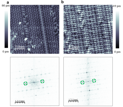
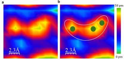
Figure A1 shows two scanning tunneling microscopy images in the {010} surface of NbTe4, with different types of columnar domain walls in the CDW superstructure. The FFT of theses images (bottom panels of A1) show the splitting on the peaks. The peaks are split for the image in figure A1(a) but not for the image in figure A1(b). Interestingly, the STM image in A1(b) has a resolution enough for identifying individual Te atoms within each cashew. Fig A2 shows the internal structure of a single cashew or Te-trimer in fig. A1(b). The three nonequivalent distances between the Nb atoms found in our theoretical model (fig 4 of the main text), give rise to an equivalent distortion on the Te atoms in the surface, as shown by figure A2b, leading to an asymmetric charge distribution within each cashew.
Figure A3 shows a representative tunneling conductance vs bias voltage curve taken at a temperature of 1.7 K. The CDW gap measured is 24 meV, similar to the CDW gap recently measured in TaTe4 at 4.2 K Sun et al. (2020).