Manipulating organic semiconductor morphology with visible light
Abstract
We present a method to manipulate the final morphology of roll-to-roll slot-die coated poly(3-hexylthiophene) (P3HT) by optically exciting the p-type polymer in solution while coating. Our results provide a comprehensive picture of the entire knowledge chain, from demonstrating how to apply our method to a fundamental understanding of the changes in morphology and physical properties induced by exciting P3HT while coating. By combining results from density functional theory and molecular dynamics simulations with a variety of X-ray experiments, absorption spectroscopy, and THz spectroscopy, we demonstrate the relationship between morphology and physical properties of the thin film. Specifically, in P3HT films excited with light during deposition, we observe changes in crystallinity and texture with more face-on orientation and increased out-of-plane charge mobility.
keywords:
Organic semiconductor, P3HT, poly(3-hexylthiophene), roll-to-roll, slot-die coating, LED light treatment, GIWAXS, GISAXS, GISANS, SAXS, WAXS, AFM, Absorbance, DFT, Solvent evaporation, coarse-grained, MARTINI, molecular dynamics, THz Spectroscopy, Organic solar cellsState-of-the-art organic photovoltaics (OPV) achieve efficiencies above 18 [1], which is competitive with their silicon counterparts [2]. However, such record solar cell efficiencies are obtained from small areas, less than 1 cm2, and fabricated with deposition methods, e.g., spin-coating, that are not compatible with large-scale production. In general, the best performing OPVs fabricated with large-scale methods such as roll-to-roll coating are trailing behind with approximately half the efficiency, i.e., 5 - 10 [3, 4]. Developing methods to close this gap is essential for a greener future.
The conjugated polymer poly(3-hexylthiophene) (P3HT) is often used as electron donor in donor-acceptor heterojunctions for OPVs [5, 6, 7, 8]. It is generally understood that the morphology of thin films of P3HT plays an important role in determining the physical and electric properties of the film [9]. Controlling the final morphology of P3HT films depends on several process parameters which include coating method, temperature, post-annealing treatments, solvents, additives, concentration, choice of substrate, gas flow above the drying film, laser treatment of film after coating, molecular weight, and regioregularity [10, 11, 12, 13, 14, 15, 16, 17, 18, 19]. Thus, optimizing the fabrication method is paramount to achieve a specific morphology and desired physical properties for best thin film performance.
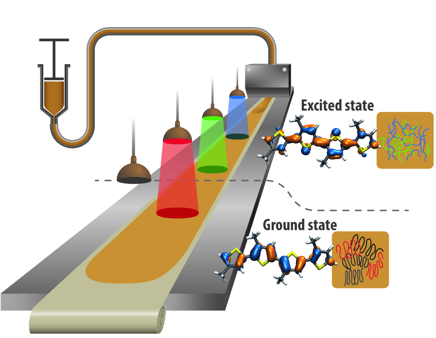
This paper presents a method to manipulate the morphology of P3HT thin films by optically exciting the polymer in solution with visible light from light-emitting diodes (LEDs) while roll-to-roll slot-die coating. Four different treatments were chosen to match energies both below and above the excitation energy levels of P3HT in solution and in thin film [20]. Specifically, either no illumination (i.e., dark), or LEDs emitting red light (625 nm), green light (525 nm), or blue light (465 nm) illuminated the films while being coated as illustrated in Figure 1. It is known from density functional theory (DFT) calculations [21] that, when exciting P3HT with visible light, i.e. going from the ground state to the excited state, the electron density changes to form double bonds between neighbouring thiophene rings as depicted in Figure 1. As discussed in the next section, this change in the bonding pattern planarizes the polymer backbone. As a consequence, the final morphology is affected when exciting the polymer during coating, which is the subject of study in this paper. To probe the morphological changes caused by the four treatments, we use Grazing-Incidence Wide-Angle X-ray Scattering (GIWAXS) on the coated films. To elucidate the physical origin of the changes, DFT and solvent evaporation molecular dynamics (MD) are used to simulate the effect of excitation on single polymer chains and thin films. The full picture of morphological changes is followed by a thorough investigation of change of physical properties in the thin film. Here, the UV-VIS absorption spectra are analyzed, followed by THz spectroscopy measuring the thin-film photo-conductivity. Finally, the consequence of light treating a complete OPV device (P3HT:O-IDTBR) is discussed.
Excitation of P3HT in solution
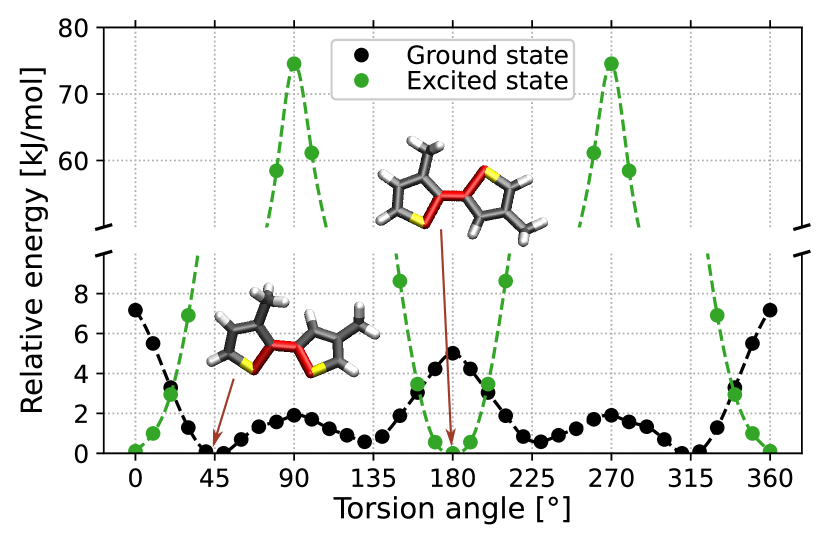
The main structural difference between the ground state (GS) and the first excited state (ES) of P3HT lies in the dihedral angles between neighboring thiophene rings. It is well known that the GS of thiophene oligomers preferentially adopts twisted geometries with equilibrium dihedral angles around 45∘, whereas the excited states are perfectly planar [21]. The torsional profiles obtained from relaxed scans performed on 3-methylthiophene (3MT) dimers are shown in Figure 2. In the GS, the two minima around 45∘ and 135∘ are separated by relatively low barriers of 2 kJ/mol at 90∘ and 5 kJ/mol at 180∘, which can be overcome at room temperature ( 2.5 kJ/mol at 300K). This ease of rotation between monomers confers a rather large conformational freedom to P3HT chains in the GS. In contrast, the ES torsional profile has minima at 0∘ (cis conformation) and 180∘ (trans conformation) separated by much higher barriers of 75 kJ/mol, which essentially lock the dimer in one of the two co-planar conformations. This difference between the GS and ES torsional profiles is due to the electronic structure. As in many conjugated polymers, the to transition is due mainly to HOMO to LUMO excitation, as shown in Figure 1, and is accompanied by an aromatic to quinoid electronic rearrangement [21]. The electronic density shifts from the intra-ring aromatic system to the inter-ring bonds, which acquire a more pronounced double bond character that inhibits rotation. It is reasonable to assume that the gas-phase torsional potential of the excited 3MT dimer, presented in Figure 2, is a good approximation of P3HT in solution. From transmission Small Angle X-ray Scattering (SAXS) it is observed that keeping P3HT in the dark, i.e. in the ground state, the sizes of P3HT aggregates slowly increase over time. Conversely, when excited by green light, i.e. with several molecules in the excited state, the size of aggregates in solution remains constant as experimentally shown in Supplementary, Figures 2 and 3.
Excitation of P3HT during coating
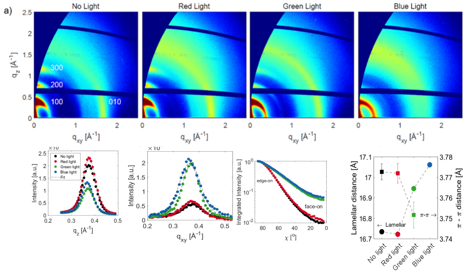
The 2D GIWAXS scattering data obtained from the four samples are shown in Figure 3a, where the lamellar stack (100, 200, and 300) and stack (010) signals are indicated. Qualitatively, we observe that the P3HT chains are predominantly oriented edge-on with respect to the substrate with a degree of orientational distribution. To quantitatively evaluate the morphological changes, the lamellar stack (100) and the stack (010) peaks are fitted by Gaussian distributions along the surface normal (qz) and in the substrate plane (qxy) with suitable background corrections , where is half the scattering angle, and is the X-ray wavelength).
In Figure 3b, the intensities of the lamellar (100) reflections are shown as a function of the reciprocal space out-of-plane distance (i.e., along the normal to the substrate) for different light treatments. The observed intensity is approximately halved in the films treated with green and blue light compared to those with no and red light. Additionally, the center of the peak is shifted to lower for the two lower intensity profiles. In real space, these observations are interpreted as an increase of the lamellar packing distance, a decrease of overall crystallinity, and a decrease of edge-on oriented aggregates when treated with green and blue light compared to the no and red light treatment.
In Figure 3c, the intensities of the lamellar (100) reflections are shown as a function of the reciprocal space in-plane coordinate (i.e. in the substrate plane) for different light treatments. The observed intensities increase drastically in the films treated with green and blue light, approximately four times more intense than the other two treatments. This observation indicates a significant increase of the fraction of aggregates oriented face-on with respect to the substrate.
To quantify the distribution of orientations of the lamellar with respect to the substrate, 45∘ azimuthal integrations across the lamellar peak were performed. each with an arc-width of 2∘, going from to . A Gaussian distribution is fitted to the intensity as function of for each integration. The results are shown in Figure 3d (all fits are shown in Supplementary, Figures 6-9). We observe that the distributions of of the no light and red light films are very similar to each other and strongly differ from those of the films treated with green and blue light, which are also similar to each other. This yields a predominant edge-on orientation of the crystallites. However, the samples treated with green and blue light possess a significantly higher fraction of face-on polymer chains.
In Figure 3a it can be seen that the orientation of the (010) stacking signal changes from being predominantly in-plane, , towards a higher degree of out-of-plane, , as the treatment increases in energy from no light to blue light. The in-and out-of-plane line integrations of the stacking signals are shown in Supplementary, Figure 5. In Figure 3e the real space in-plane stack (010) and the out-of-plane lamellar stack (100) are shown. The in-plane lamellar stacking distances become larger when exposed to green and blue light, indicating less efficient packing.
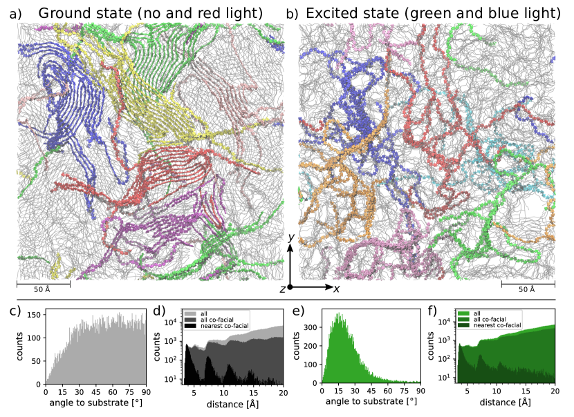
Next, we report the results of DFT calculations and MD simulations and discuss the effect of excitation on the morphology of P3HT thin films. Photoexcitation of P3HT aggregates first produces a ”hot” exciton, delocalized over few monomers, that quickly (on a time scale of 1-10 ps) decays to more delocalized ”cold” exciton that has longer lifetimes in the range of 0.1-1.0 ns [22]. This transition to the ”cold” exciton is accompanied by torsional relaxation into a more planar geometry that is a minimum of the excited state potential (see Figure 2). It is therefore reasonable to assume that continuous photoexcitation with green or blue light has the effect of keeping significant portions of the polymer chains planar on nanosecond timescales, locking the dihedral angles in either the cis or trans conformation and preventing rotation between monomers. In the MD simulation of solvent evaporation with light, for simplicity, we have chosen to keep the molecules in the ES force field all the time. This is, of course, a drastic approximation, but such an extreme model is nonetheless useful to understand the effect of excitation on morphology. The thin film morphologies obtained from the coarse-grained MD simulations of solvent evaporation without and with light (using the GS and ES force field, respectively) are shown in Figure 4. The two morphologies are strikingly different: the GS sample consists mainly of lamellar aggregates typical of P3HT, consisting of roughly 10 -stacked chain sections of about 25 monomers. The ES film appears much more disordered from the top, i.e., when viewed along the z direction normal to the substrate (right panel of 4). A more detailed examination reveals that in the ES sample, most molecules form stacks in the z direction but do not form large lamellae as in the GS sample. Instead, each chain tends to participate in multiple smaller aggregates with short sections of 5-10 monomers. The GS sample presents more efficient packing than the ES sample, with final densities of 1.13 and 1.05 g/mL, respectively.
The distributions of angles between the thiophene rings and the substrate (xy plane) are shown in Figure 4c and 4e. In the GS film, the distribution of angles is rather flat, indicating almost isotropic orientation, with 21 of the rings face-on (angle 30∘). In contrast, in the ES film 77% of the rings are within 30∘ of the xy plane: this strong prevalence of face-on orientation, although possibly exaggerated by keeping all chains excited all the time, the trend is consistent with the GIWAXS data in Figure 3. Figure 4d and 4f are the distributions of distances between all ring centers and two subsets thereof (see legend): those which are co-facial to each other (angle 30∘) and only the nearest co-facial neighbors. The first peak at around 3.75 Å is composed exclusively of stacked nearest neighbors and is very similar in the two samples. Similar stacking distances are observed with GIWAXS as shown in Figure 3e, although we cannot detect its average decrease in the MD morphologies. The successive peaks are at multiples of this distance and are less pronounced in the ES sample. The GS sample presents pronounced co-facial non-neighboring peaks at 7.5, 11.25, 15.0, and 18.75 Å, which are multiples of the stacking distance and are clearly originating from the lamellar aggregates. The peak at 5.25 Å does not appear among the nearest neighbors and is of unclear origin. A much larger proportion of rings are co-facial in the ES sample because their orientation is prevalently face-on. Still, all non-neighboring peaks are almost absent, indicating a less crystalline structure than the GS sample, in agreement with the observations from GIWAXS.
Finally, the surface roughness of the four samples was obtained from atomic force microscopy. The results, shown in Supplementary, Figure 12, indicate roughness of 20.0, 9.8, 2.7, and 4.2 nm for no, red, green, and blue light, respectively. This decrease in roughness points to an overall reduction of crystallinity and more homogeneous morphology as a consequence of light treatment, consistent with the GIWAXS and MD results.
Dynamics of Physical properties
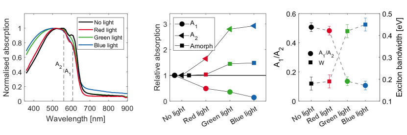
Normalized UV-VIS absorption spectra are shown in Figure 5a with dashed lines indicating the absorption peaks and . A broadening of the absorption into lower wavelength regime is observed for green and blue light treatment. It is thought that intrachain excitons in disordered chains cause such broadening [23]. The absorption spectra are modelled to four Gaussian distributions, where the integrated intensities of and are shown in Figure 5b, where the remaining two contributions are labeled as amorphous [24] (more details are found in Supplementary Figure 10). In Figure 5b, the ratios of and are shown with respect to the no light treatment reference sample. Here, large and similar changes in absorption intensity, and , are observed for green and blue light treatments. Unexpected, a slight change in the relative absorption in the red light treated film is observed, can be caused be the large bandwidth of the LED light. To interpret the observed changes in the absorption spectra, we adopt the weakly interacting H-aggregate model [25, 23, 26], according to which the ratio between the fitted values of the absorption intensities and reads
| (1) |
In eq. (1), is the free-exciton bandwidth of the aggregates, where is the Coulombic inter-chain electronic coupling. = 0.18 eV is the energy of the C=C symmetric stretching, assumed to be the main intramolecular vibration coupled to the electronic transition [25, 27] and the corresponding Huang-Ryhs factor is assumed to be 1. The ratios and the corresponding values of obtained from eq. (1) are shown in Figure 5c, and the exact numbers and errors are provided in Supplementary Table 2. The inter-chain coupling , and consequently , is known to decrease with increasing conjugation length[27]. The increase of , observed when going from no and red light to green and blue light treatment, indicates a decrease of conjugation length consistent with a more disordered morphology with smaller and fewer aggregates.
Correlation of structure and conductivity
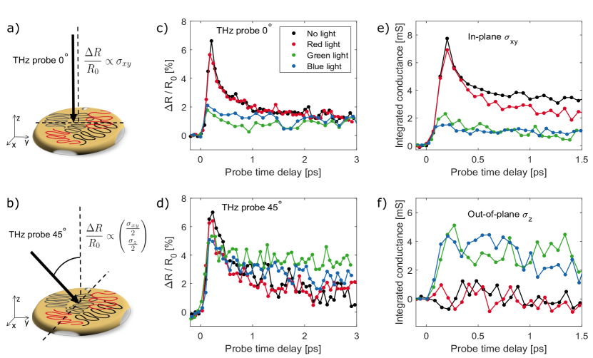
Time-resolved terahertz spectroscopy (TRTS) is a powerful tool for investigating ultrafast charge carrier transportation dynamics in organic materials at a characteristic length scale on the order of 10 nm [28, 29]. A THz wave is always polarized perpendicularly to its propagation direction, and therefore only charge carrier motion in directions perpendicular to the THz beam are probed. To probe both in-plane and out-of-plane charge carrier dynamics, reflection-mode TRTS measurements were performed with two different incidence angles onto the P3HT films. At normal incidence angle only the in-plane photo-conductivity is picked up; at 45∘ incidence angle both in-plane and out-of-plane conductivities can be extracted from the total conductivity , as illustrated in Figure 6a and 6b.
In Figures 6c and 6d., the time evolutions of the transient THz wave reflection , caused by photoexcitation of the film, were measured for all four samples at both 0∘ and 45∘. At normal incidence (probing in-plane mobility), the no light and red light treatment yield much stronger transient responses, with fast trapping of hot carriers. In contrast, the green and blue light treatment yield a much weaker in-plane response, and the trapping is more moderate. Probing with a 45° configuration, the green light and blue light treatments lead to a dramatic increase in transient response. In contrast, the no light and red light only show minor changes compared to the normal incidence configuration.
Full 2D TRTS scans (see Supplementary Figures 17-19) were performed to get explicit information about the photo-conductivity of the films. Sheet conductances were obtained by spectral integration of the 2D scans in the 2 to 12 THz frequency range. The in-plane conductance , obtained from the normal incidence scan, is shown in Figure 6e. The out-of-plane conductance component extracted from the 45∘ scan, , is shown in Figure 6f. The contrast between the two groups of light treatment is pronounced: whereas the no and red light films predominantly exhibit in-plane photo-conductivity, the green and blue light treated films strongly favor out-of-plane charge transport. Since conductance in polymers is limited by inter-chain transport, i.e., along the -stacking direction in semi-crystalline P3HT, this clear result strongly confirms the prevalence of aggregates oriented edge-on in the no and red light films and face-on in the green and blue light films, as observed by our GIWAXS measurements and MD simulations.
Technological Impact
The experimental and computational results presented in this paper demonstrate that exciting P3HT with visible light during deposition serves as a tool for manipulating the packing behavior of P3HT and can be used to modify the final thin film morphology. It can be considered a new processing parameter for achieving the desired performance of organic thin films. Particularly, the capability to increase the out-of-plane mobility by light treatment can be used for transistor applications where directional mobility and patterning is essential [30]. In a poor solvent for P3HT, such as ortho-xylene, the light treatment will not prevent P3HT from forming aggregates over time (see Supplementary, Figure 4). Investigating the many aspects of optimization to determine the optimal wavelength for treating a polymer in combination with temperature and solvents will be a full study of its own. Furthermore, optimizing OPV devices comes with an additional challenge when two constituents require optimization processes for the right crystal packing and domain size. For the specific combination P3HT:O-IDTBR, the domain size decreases with light treatment and still results in a decrease in power conversion efficiency, as shown in Supplementary, Figures 13-15. However, understanding how light treatment during fabrication influences the final morphology of a film can enable major improvements for specific materials systems or other technologies in flexible electronics.
In conclusion, we report a method to manipulate the morphology of P3HT thin films through illumination with visible LED light during roll-to-roll slot-die coating. Optical polymer excitation temporarily constrains large sections of the chains into a planar geometry that is the minimum of the excited state potential energy surface. This structural effect is strong enough to affect the aggregation behavior and, thereby, the final morphology of the P3HT film. The light-treated films are less crystalline overall, display a higher degree of face-on orientation, shorter conjugation length, and a change of the unit cell dimensions with less efficient packing. Consequently, the in-plane photo-conductivity decreases and the out-of-plane conductivity increases drastically with light treatment.
The authors acknowledge financial support from the H2020 European Research Council through the SEEWHI Consolidator grant, ERC-2015-CoG-681881 and from the Independent Research Fund Denmark, grant no. 0200-00001B. Danscatt for travel expenses during beam times: DESY proposal number 15559230912. SAXS measurements were carried out at the P03/MiNaXS beamline, PETRA III at DESY. Neutron beam time at MLZ, proposal-15551”. Some WAXS experiments were carried out at the cSAXS beamline, Paul Scherrer Institute, Switzerland, proposal number 20182246. Deuterated SD-P3HT was synthesized at the Center for Nanophase Materials Sciences, which is a DOE Office of Science User Facility (CNMS Proposal ID: CNMS2020-R-00546), Kristian Larsen for countless hours of technical support.
References
- [1] Qishi Liu et al. “18% Efficiency organic solar cells” In Science Bulletin 65.4 Elsevier B.V., 2020, pp. 272–275 DOI: 10.1016/j.scib.2020.01.001
- [2] Martin A. Green et al. “Solar cell efficiency tables (Version 58)” In Progress in Photovoltaics: Research and Applications 29.7 John Wiley & Sons, Ltd, 2021, pp. 657–667 DOI: 10.1002/PIP.3444
- [3] Anders S. Gertsen, Marcial Fernández Castro, Roar R. Søndergaard and Jens W. Andreasen “Scalable fabrication of organic solar cells based on non-fullerene acceptors” In Flexible and Printed Electronics 5.1 IOP Publishing, 2020, pp. 014004 DOI: 10.1088/2058-8585/AB5F57
- [4] Guodong Wang et al. “Synergistic Optimization Enables Large-Area Flexible Organic Solar Cells to Maintain over 98% PCE of the Small-Area Rigid Devices” In Advanced Materials 32.49 John Wiley & Sons, Ltd, 2020, pp. 2005153 DOI: 10.1002/adma.202005153
- [5] Enrique Pascual-San-José et al. “Blade coated P3HT:non-fullerene acceptor solar cells: a high-throughput parameter study with a focus on up-scalability” In Journal of Materials Chemistry A 7.35 Royal Society of Chemistry (RSC), 2019, pp. 20369–20382 DOI: 10.1039/c9ta07361b
- [6] Sarah Holliday et al. “High-efficiency and air-stable P3HT-based polymer solar cells with a new non-fullerene acceptor” In Nature Communications 7, 2016, pp. 1–11 DOI: 10.1038/ncomms11585
- [7] Derya Baran et al. “Reducing the efficiency-stability-cost gap of organic photovoltaics with highly efficient and stable small molecule acceptor ternary solar cells” In Nature Materials 16.3, 2017, pp. 363–369 DOI: 10.1038/nmat4797
- [8] Ning Li et al. “Environmentally printing efficient organic tandem solar cells with high fill factors: A guideline towards 20% power conversion efficiency” In Advanced Energy Materials 4.11 Wiley-VCH Verlag, 2014 DOI: 10.1002/AENM.201400084
- [9] Sabine Ludwigs “P3HT Revisited-from Molecular Scale to Solar Cell Devices” Springer, Berlin, Heidelberg, 2014, pp. 232 DOI: https://doi.org/10.1007/978-3-662-45145-8
- [10] Dean M. et al. “Variations in Semiconducting Polymer Microstructure and Hole Mobility with Spin-Coating Speed” In Chemistry of Materials 17.23, 2005, pp. 5610–5612 DOI: 10.1021/cm0513637
- [11] Tobias Rödlmeier et al. “Controlled Molecular Orientation of Inkjet Printed Semiconducting Polymer Fibers by Crystallization Templating” In Chemistry of Materials 29.23 American Chemical Society, 2017, pp. 10150–10158 DOI: 10.1021/ACS.CHEMMATER.7B03948/SUPPL–“˙˝FILE/CM7B03948–“˙˝SI–“˙˝002.AVI
- [12] Benjamin Schmidt-Hansberg et al. “Moving through the phase diagram: Morphology formation in solution cast polymer-fullerene blend films for organic solar cells” In ACS Nano 5.11, 2011, pp. 8579–8590 DOI: 10.1021/nn2036279
- [13] Natalia K. Zawacka et al. “The influence of additives on the morphology and stability of roll-to-roll processed polymer solar cells studied through ex situ and in situ X-ray scattering” In Journal of Materials Chemistry A 2.43 Royal Society of Chemistry, 2014, pp. 18644–18654 DOI: 10.1039/c4ta03484h
- [14] Kerstin S Wienhold et al. “Effect of Solvent Additives on the Morphology and Device Performance of Printed Nonfullerene Acceptor Based Organic Solar Cells” In ACS Applied Materials and Interfaces 11(45), 2019, pp. 42313–42321 DOI: 10.1021/acsami.9b16784
- [15] Daisuke Kajiya and Ken Ichi Saitow “Ultrapure Films of Polythiophene Derivatives are Born on a Substrate by Liquid Flow” In ACS Applied Energy Materials 1.12, 2018, pp. 6881–6889 DOI: 10.1021/acsaem.8b01260
- [16] Lin Feng et al. “Laser-induced crystallization and conformation control of poly ( 3- hexylthiophene ) for improving the performance of organic solar cells Laser-induced crystallization and conformation control of poly ( 3- hexylthiophene ) for improving the performance of” In Organic Electronics 49.June Elsevier B.V, 2017, pp. 157–164 DOI: 10.1016/j.orgel.2017.06.053
- [17] Jafar Iqbal Khan et al. “P3HT Molecular Weight Determines the Performance of P3HT:O-IDTBR Solar Cells” In Solar RRL 3.8 John Wiley & Sons, Ltd, 2019, pp. 1900023 DOI: 10.1002/solr.201900023
- [18] H. Sirringhaus et al. “Two-dimensional charge transport in self-organized, high-mobility conjugated polymers” In Nature 1999 401:6754 401.6754 Nature Publishing Group, 1999, pp. 685–688 DOI: 10.1038/44359
- [19] Stephen G Urquhart et al. “Connecting Molecular Conformation to Aggregation in P3HT Using Near Edge X-ray Absorption Fine Structure Spectroscopy” In J. Phys. Chem. C, 2017, pp. 121 DOI: 10.1021/acs.jpcc.7b07143
- [20] Khosrow Rahimi et al. “Light absorption of poly(3-hexylthiophene) single crystals †” In Open Access Article. Published on 4, 2014, pp. 11121–11123 DOI: 10.1039/c3ra47064d
- [21] Ras Baizureen Roseli, Patrick C. Tapping and Tak W. Kee “Origin of the Excited-State Absorption Spectrum of Polythiophene” In Journal of Physical Chemistry Letters 8.13 American Chemical Society, 2017, pp. 2806–2811 DOI: 10.1021/ACS.JPCLETT.7B01053/SUPPL–“˙˝FILE/JZ7B01053–“˙˝SI–“˙˝001.PDF
- [22] Oleg P. Dimitriev, David A. Blank, Christian Ganser and Christian Teichert “Effect of the Polymer Chain Arrangement on Exciton and Polaron Dynamics in P3HT and P3HT:PCBM Films” In Journal of Physical Chemistry C 122.30, 2018, pp. 17096–17109 DOI: 10.1021/acs.jpcc.8b05155
- [23] Jenny Clark et al. “Determining exciton bandwidth and film microstructure in polythiophene films using linear absorption spectroscopy” In Applied Physics Letters 94.16, 2009 DOI: 10.1063/1.3110904
- [24] Kshitij Bhargava, Mayoorika Shukla and Vipul Singh “Comparative analysis of contact resistance and photoresponse in poly(3-hexylthiophene) and poly(3-octylthiophene) based organic field-effect transistors” In Synthetic Metals 233 Elsevier, 2017, pp. 15–21 DOI: 10.1016/j.synthmet.2017.08.013
- [25] Frank C. Spano “Modeling disorder in polymer aggregates: The optical spectroscopy of regioregular poly(3-hexylthiophene) thin films” In Journal of Chemical Physics 122.23 American Institute of PhysicsAIP, 2005, pp. 234701 DOI: 10.1063/1.1914768
- [26] Kshitij Bhargava and Vipul Singh “Investigation of Gold and Poly(3-Alkylthiophene) interface in top and bottom contact structures” In Synthetic Metals 211 Elsevier, 2016, pp. 49–57 DOI: 10.1016/j.synthmet.2015.11.003
- [27] Frank C. Spano and Carlos Silva “H- and J-aggregate behavior in polymeric semiconductors” In Annual Review of Physical Chemistry 65 Annual Reviews, 2014, pp. 477–500 DOI: 10.1146/annurev-physchem-040513-103639
- [28] D.. Cooke, F.. Krebs and P.. Jepsen “Direct observation of sub-100 fs mobile charge generation in a polymer-fullerene film” In Physical Review Letters 108.5 American Physical Society, 2012, pp. 056603 DOI: 10.1103/PhysRevLett.108.056603
- [29] Nenad Vukmirović et al. “Insights into the charge carrier terahertz mobility in polyfluorenes from large-scale atomistic simulations and time-resolved terahertz spectroscopy” In Journal of Physical Chemistry C 116.37, 2012, pp. 19665–19672 DOI: 10.1021/jp3055262
- [30] Jesper Edberg et al. “Patterning and Conductivity Modulation of Conductive Polymers by UV Light Exposure” In Advanced Functional Materials 26.38 John Wiley & Sons, Ltd, 2016, pp. 6950–6960 DOI: 10.1002/adfm.201601794
- [31] Jacek Jakowski et al. “Deuteration as a Means to Tune Crystallinity of Conducting Polymers” In The Journal of Physical Chemistry Letters 8.18, 2017, pp. 4333–4340 DOI: 10.1021/acs.jpclett.7b01803
- [32] Michael Korning Sørensen et al. “In situ grazing incidence small angle x-ray scattering on roll-to-roll coating of organic solar cells with laboratory x-ray instrumentation” In Journal of Visualized Experiments 2021.169 Journal of Visualized Experiments, 2021, pp. 1–22 DOI: 10.3791/61374
- [33] M.. Frisch et al. “Gaussian16 Revision C.01”, 2016
- [34] Paulo C.T. Souza et al. “Martini 3: a general purpose force field for coarse-grained molecular dynamics” In Nature Methods 18.4, 2021, pp. 382–388 DOI: 10.1038/s41592-021-01098-3
- [35] Anders S Gertsen “Multiscale Modelling of Organic Solar Cell Materials”, 2020, pp. 185
- [36] Anders S. Gertsen “Molecular dynamics force fields for organic solar cell materials”, 2021 DOI: https://doi.org/10.11583/DTU.c.5254236.v1
- [37] Cheng Kuang Lee and Chun Wei Pao “Nanomorphology evolution of p3ht/pcbm blends during solution-processing from coarse-grained molecular simulations” In Journal of Physical Chemistry C 118.21 American Chemical Society, 2014, pp. 11224–11233 DOI: 10.1021/JP501323P/SUPPL–“˙˝FILE/JP501323P–“˙˝SI–“˙˝001.PDF
- [38] Riccardo Alessandri et al. “Bulk Heterojunction Morphologies with Atomistic Resolution from Coarse-Grain Solvent Evaporation Simulations” In Journal of the American Chemical Society 139.10 American Chemical Society, 2017, pp. 3697–3705 DOI: 10.1021/jacs.6b11717
- [39] Anders S Gertsen, Michael Korning Sørensen and Jens W Andreasen “Nanostructure of organic semiconductor thin films: Molecular dynamics modeling with solvent evaporation” In Physical Review Materials 4.7, 2020 DOI: 10.1103/PhysRevMaterials.4.075405
- [40] Tsjerk A. Wassenaar et al. “Going backward: A flexible geometric approach to reverse transformation from coarse grained to atomistic models” In Journal of Chemical Theory and Computation 10.2 American Chemical Society, 2014, pp. 676–690 DOI: 10.1021/CT400617G/SUPPL–“˙˝FILE/CT400617G–“˙˝SI–“˙˝002.TXT
- [41] Michael Gaus, Albrecht Goez and Marcus Elstner “Parametrization and benchmark of DFTB3 for organic molecules” In Journal of Chemical Theory and Computation 9.1, 2013, pp. 338–354 DOI: 10.1021/ct300849w
- [42] Michael Gaus, Xiya Lu, Marcus Elstner and Qiang Cui “Parameterization of DFTB3/3OB for sulfur and phosphorus for chemical and biological applications” In Journal of Chemical Theory and Computation 10.4, 2014, pp. 1518–1537 DOI: 10.1021/ct401002w
- [43] “AMS DFTB 2021.1, SCM, Theoretical Chemistry Vrije Universiteit Amsterdam The Netherlands http://www.scm.com”, 2021
- [44] G. Velde et al. “Chemistry with ADF” In Journal of Computational Chemistry 22.9, 2001, pp. 931–967 DOI: 10.1002/JCC.1056/FORMAT/PDF
- [45] Robert Rüger et al. “Efficient calculation of electronic absorption spectra by means of intensity-selected time-dependent density functional tight binding” In Journal of Chemical Theory and Computation 11.1 American Chemical Society, 2015, pp. 157–167 DOI: 10.1021/ct500838h
- [46] Dag W Breiby et al. “Simulating X-ray diffraction of textured films” In J. Appl. Cryst 41, 2008, pp. 262–271 DOI: 10.1107/S0021889808001064
- [47] Adeline Buffet et al. “P03, the microfocus and nanofocus X-ray scattering (MiNaXS) beamline of the PETRA III storage ring: The microfocus endstation” In Journal of Synchrotron Radiation 19.4, 2012, pp. 647–653 DOI: 10.1107/S0909049512016895
- [48] Gunthard Benecke et al. “A customizable software for fast reduction and analysis of large X-ray scattering data sets: applications of the new DPDAK package to small-angle X-ray scattering and grazing-incidence small-angle X-ray scattering” In J. Appl. Cryst 47.5 International Union of Crystallography, 2014, pp. 1797–1803 DOI: 10.1107/S1600576714019773
- [49] Stefan Mattauch et al. “The high-intensity reflectometer of the jülich centre for neutron science: MARIA” In Journal of Applied Crystallography 51, 2018, pp. 546–654 DOI: 10.1107/S1600576718006994
- [50] Marcial Fernández Castro et al. “Flexible ITO-Free Roll-Processed Large-Area Nonfullerene Organic Solar Cells Based on P3HT:O-IDTBR” In Physical Review Applied 14.3 American Physical Society, 2020, pp. 034067 DOI: 10.1103/PhysRevApplied.14.034067
1 Materials and Methods
All P3HT, Poly(3-hexylthiophene-2,5-diyl), in this work were purchased from Osilla: Lot number M1011, with a molecular weight Mw = 60.15 kDa, and a regioregularity of RR = 96.76 . All solutions were prepared with dichlorobenzene (99.0 ) with 20 mg/mL of P3HT and were stirred for 12 hours at 60 ∘C until fully dissolved. A deuterated version, SD-P3HT, was synthesized at the Center for Nanophase Materials Sciences and the same batch as presented by Kunlun et. al.[31]. O-IDTBR is purchased from 1-Material Inc. Silicon (100) and glass substrates were initially cleaned for 30 min in an ultrasonic bath: 10 min in isopropanol, 10 min in acetone, and 10 min in demineralized water. The slot-die coating procedure was done by mounting the rigid substrate of either silicon or glass on top of PET that were then running roll-to-roll while coating. This procedure can be found in a video article [32], where the pumping rate is 0.08 mL/min, the speed of the substrate is 1 cm/min, and the width of the film 1 cm. We obtained a dry film of P3HT with thickness 210 nm ( 20 nm) and length limited by the substrate dimensions, here 5-10 cm. All samples were coated at room temperature (approximately 22 ∘C) in a fume hood. When the full length of the substrate had been coated, the syringe pump was stopped and the substrate kept moving the sample an additional 7 cm to the rest station. At the rest station the samples were exposed to either red, green, blue, or no light for 10 minutes. All other lights in the lab were turned off during the samples’ preparation. For the light exposed samples three LEDs (3W LED, on PCB) with 1.5 cm spacing were placed 4 cm above the samples. The LEDs were connected in series and a direct current of 1 Ampere and a voltage of 9 volts was applied. For all samples, the slot-die head was placed 7 cm from the sustrate. The temperature of the substrate remained constant during the light treatment.
1.1 Computational methodology
Classical molecular dynamics (MD) simulations were performed to generate plausible morphologies of solution-processed P3HT films deposited in absence and in presence of visible light illumination. To simulate the effect of light-induced electronic excitation on molecular geometry and therefore film morphology we derived two distinct force fields for the GS and ES of P3HT. A force field for the GS of P3HT was derived from the existing OPLS-AA (Optimized Potentials for Liquid Simulations - All Atom) force field and refined where needed with ab initio density functional theory (DFT) calculations on 3MT (3-methyl-thiophene) oligomers. The atomic charges and a few structural parameters (inter-monomer bond length, angles within the backbone) were obtained from geometry optimization of a P3MT 8-mer at the B3LYP/6-311++G(d,p) level of theory using Gaussian 16[33]. The atomic charges were obtained by fitting to the electrostatic potential (ESP) with the CHELPG scheme implemented in Gaussian 16 and then rescaled to yield net zero charge on internal monomers and equal charges of opposite sign on the terminal monomers. The proper dihedral angles between monomers were modelled with a Ryckaert-Bellemans (RB) functional form. The RB coefficients were obtained by fitting to the torsional profile of a 3MT dimer calculated at the B97X-D/6-311++G(d,p) level of theory. The torsional profile (energy as a function of the dihedral angle) was calculated with a relaxed scan, i.e. a series of geometry optimizations with the dihedral angle constrained to fixed values between 0∘ and 180 ∘. To simulate the effect of illumination with classical MD, we built a different force field for the first ES of P3HT. The ESP atomic charges were obtained from geometry optimization of the first ES of a 3MT 8-mer with TDDFT/B3LYP/6-311++G(d,p) and then rescaled with the same procedure as for the GS. The inter-monomer dihedral angle parameters were obtained with the same procedure as for the GS, but the torsional profile was obtained from a relaxed scan performed on the first ES of a 3MT dimer calculated at the TDDFT/B97X-D/6-311++G(d,p) level of theory. All other ES force field parameters are identical to the GS force field. Coarse-grained (CG) force fields, where several atoms are represented by one larger particle (bead), have the goal of reducing the number of particles in the simulation and thereby dramatically increase the system size and/or simulation length achievable with given computational resources. Here we adopt a MARTINI 3.0 [34] CG model of P3HT [35] [36] based on the OPLS-AA force field described above. In the CG model the thiophene ring is represented by three tiny beads of type TC6, TC5 and TC5 with constraints between them to keep the ring rigid. One virtual site (VS) is placed at the center of geometry (COG) of the ring. The alkyl chain is connected to the ring by a harmonic bond and is represented by two small beads of type SC2, also connected by a harmonic bond. The chlorobenzene molecule is represented by three beads with constrained bonds: two of type TC5 and one of type SX3. A visual representation of the CG mapping is shown in Supplementary Figure 1. The GS and ES CG force fields differ only by the inter-monomer dihedral angle parameters, which were taken from the OPLS-AA force fields described above. The CG model and force field of chlorobenzene was described in ref. [35].
P3HT thin film morphologies were generated using a previously published solvent evaporation scheme based on CG MD simulations where the solvent molecules are progressively removed from the simulation box until none are left, mimicking the drying of a thin film deposited in a slot-die coating process [37, 38, 39]. The same simulation was run both with the GS and the ES CG force fields, with all other conditions identical. The initial configuration of the system was prepared by randomly placing 420 P3HT 48-mers in a periodic simulation box of initial dimensions 25 x 25 x 136.7 nm and solvating them with 469725 chlorobenzene molecules, yielding a concentration of around 40 mg/mL. The system was first equilibrated for 0.5 ns in an NVT ensemble and then for 4.0 ns in an NPT ensemble. After this, the evaporation run was started: at each step, 1.25 of the remaining solvent molecules, randomly selected, were removed from the box. After reaching the near-linear regime, i.e. when less than 0.0125 of the initial amount of solvent was removed at each step, the evaporation was continued linearly (removing the same number of molecules each step) until a dry film (without solvent) was obtained, amounting to a total of 264 steps. At each step, after removing the solvent the system was equilibrated for 0.5 ns in an NVT ensemble (Berendsen thermostat, coupling constant = 2 ps) and for 4.0 ns in an NPT ensemble (Berendsen thermostat, = 2 ps, and Berendsen barostat, = 4 ps) before undergoing a production run of 3.0 ns in an NPT ensemble (Berendsen thermostat, = 2 ps, Parrinello-Rahman barostat, = 15 ps), adding up to a total evaporation time of around 2 s. A 20 fs time step was used for the leap-frog integrator, and semi-isotropic pressure coupling was applied with a pressure of 1 bar and a compressibility of bar-1 in the z-direction and of 0.0 bar-1 in the textitx- and y-directions to facilitate shrinking of the box only in the z-direction, hence mimicking the conditions in a drying thin film. No charges were present in the systems, meaning that the electrostatics could be ignored. The van der Waals interactions were treated with the potential-shift Verlet scheme with a cut-off of 1.1 nm as recommended for MARTINI force fields. From each of the two final thin film morphologies, two aggregates of 8 48-mers were selected for the calculation of UV-Vis absorption energies. First, the aggregates were back-mapped to atomistic resolution with the backward method described in ref [40] using an initial random displacement (”kick”) of 0.35 nm. The geometries of the resulting back-mapped aggregates were then optimized with GROMACS using the GS OPLS-AA force field and non-aggregated portions of the molecules were removed to obtain 8 24-mers (6 24-mers and 1 48-mer in one of the ES aggregates). To further reduce the atom count, the hexyl side chains were substituted with methyls, since sp3 side chains have little influence on the electronic structure of the excited states. Excited state calculations on systems of this size (1900 atoms) are not feasible with TDDFT, therefore we computed the single point electronic structure with the semi-empirical DFTB3 method with the 3ob-3-1 parameter set [41, 42] using the DFTB engine of the AMS 2020 program suite[43, 44]. The energies and oscillator strengths of the lowest 60 singlet excitations were calculated with the TD-DFTB method [45] as implemented in AMS DFTB. The computed absorption spectra shown in Supplementary, Figure 11, were obtained by combining the excitations of two aggregates from each of the thin film morphologies and convoluted with Gaussian functions of width 3.0 nm and weights corresponding to the oscillator strengths.
1.2 Experimental methodology
1.2.1 Absorption and External quantum efficiency
Absorption spectroscopy and External quantum efficiencies (EQE) as function of incident wavelength where obtained by using a QEX10 system (PV Measurements Inc.). For all measurements the incident wavelength were probed from 300 to 900 nm in steps of 5 nm. The system is calibrated with a Si photo diode.
1.2.2 GIWAXS
To perform Grazing Incidence Wide-Angle X-ray Scattering (GIWAXS) measurements, a laboratory setup was used (Xeuss 3.0 from Xenocs S.A.). Here, supplied with a microfocus copper source, Cu K α radiation (waveleng () = 1.5418 Å) is focused and monochromatized with a two-dimensional single reflection multilayer optic and collimated with scatterless slits. The silicon substrate surface was aligned at a grazing incident angle of 0.18° with respect to the incoming X-ray beam. The scattered X-ray were detected on an Eiger 4M single photon counting detector, with 75 µm pixels (DECTRIS), 90.0 mm from the sample. Conversion of the raw 2D data to reciprocal space coordinates was performed with the SimDiffraction MATLAB script package [46].
1.2.3 Time-resolved THz spectroscopy
For the transient optical-pump THz-probe spectroscopy investigation, 2 mJ, 40 fs pulses with 1 kHz repetition rate, 800-nm central wavelength from a Ti:sapphire laser amplifier (Spectra-Physics, Spitfire Ace) are split into three beams for terahertz wave generation, waveform detection, and for generating the optical excitation pulses at 400 nm, respectively. The ultra-broadband THz pulse generation is realized by 2-colour fs laser induced air-plasma process in the focal zone of the fundamental driving laser beam (800 nm) and its second harmonic beam. To preserve the ultra-broad THz bandwidth from the generation process, an air-biased coherent detection (ABCD) scheme was implemented. The 400-nm optical excitation beam was projected onto the sample with 1.4 mm diameter (full width half maximum) spot size in the normal incident case. For the 45° incidence configuration, the spot onto the tilted sample is larger (1.414 times). We use same pump fluence of 585 for all the measurements, which is slightly below the damage threshold of the polymer films.
1.2.4 Atomic Force Microscopy
To obtain the surface morphologies of the layers, the scanning probe microscopy (DualScopeTM scanner DS 95-50 with a DualScopeTM controller C-26, DME) was used with Si tips (ArrowTM NCR, NanoWorld) at room temperature. The spring constant of the tip is 42 N/m, and the curvature radius is below 10 nm. Thin film where prepared on Si (100) wafers and cut in appropriate sizes ( cm2).
1.2.5 SAXS
Small Angle X-ray Scattering (SAXS) in transmission mode measurements where performed at DESY, P03 at the microfocused end-station [47]. The energy was chosen to be 11.2 keV and a sample to detector distance calibrated with AgBeh to be at 3900 mm. The scattered X-ray are detected by a Pilatus 300k pixel detector. To load the data and perform flat-field correction, DPDAK software was used [48].
1.2.6 GISANS
Grazing Incidence Small-Angle Neutron Scattering (GISANS) measurements where performed at MARIA beam line at FRM2 [49], with a probing wavelength of 10 Å unpolarized neutrons with a sample to detector distance of 1910 mm. The incident angle where optimized at the reflected neutron beam at 0.52∘.
1.2.7 Organic Solar Cells
The fabrication procedure is outside the scope of the paper, and can be found in [50]. The Device structure is the PET/ITO/ZnO/P3HT:O-IDTBR/MoO/Ag. While coating the active layer (P3HT:O-IDTBR), the inks where exposed to either no, red, green, and blue light. All current density-voltage (J -V) curves are measured using a solar simulator with a xenon lamp as the light source, which is calibrated by a certified reference cell (monocrystalline silicon certified by Fraunhofer) under AM1.5G illumination, 1000 W/m2 intensity, and acquired by a Keithley 2400 source meter (25 mV step reverse to forward). No current is obtained outside the solar-cell area, as the flextrode is cut to ensure 1 cm2 devices.