subsecref \newrefsubsecname = \RSsectxt \RS@ifundefinedthmref \newrefthmname = theorem \RS@ifundefinedlemref \newreflemname = lemma
Magnetism and Interlayer Bonding in Pores of Bernal-Stacked Hexagonal Boron Nitride
Abstract
When single-layer h-BN is subjected to a high-energy electron beam, triangular pores with nitrogen edges are formed. Because of the broken bonds, these pores are known to possess magnetic states. We report on the magnetism and electronic structure of triangular pores as a function of their size. Moreover, in the Bernal-stacked h-BN (AB-h-BN), multilayer pores with parallel edges can be created, which is not possible in the commonly fabricated multilayer -h-BN. Given that these pores can be manufactured in a well-controlled fashion using an electron beam, it is important to understand the interactions of pores in neighboring layers. We find that in certain configurations, the edges of the neighboring pores remain open and retain their magnetism, and in others, they form interlayer bonds. We present a comprehensive report on these configurations for small nanopores. We find that at low temperatures, these pores have near degenerate magnetic configurations, and may be utilized in magnetoresistance and spintronics applications. In the process of forming larger multilayer nanopores, interlayer bonds can form, reducing the magnetization. Yet, unbonded parallel multilayer edges remain available at all sizes. Understanding these pores is also helpful in a multitude of applications such as DNA sequencing and quantum emission.
I Introduction
Low-dimensional materials enable a wide range of uses not possible with bulk (three-dimensional) materials. Creating holes in two-dimensional (2D) materials, in particular, allows for applications like molecular sieving, metamaterials, and quantum emission (Koenig et al., 2012; Choi et al., 2016; Zhao et al., 2019; Caldwell et al., 2019; Liu et al., 2021; Song et al., 2021). Researchers can tailor a system for a specific application by controlling the size, shape, and/or distribution of holes in a 2D material. DNA sequencing using nanopores (holes as small as a few nm) is one example of such an application, which would allow for quick and precise sequencing of single unbroken DNA strands (Liu et al., 2013; Zhou et al., 2013; Muthukumar et al., 2015; Heerema and Dekker, 2016; Deamer et al., 2016). Nanopores also spontaneously form in 2D materials, so, understanding their properties is important in itself. In this study, we investigate the properties of triangular pores in single-layer hexagonal boron nitride (h-BN) and their interactions with pores in neighboring layers, which is largely determined by the stacking sequence and pore alignment. We focus primarily on Bernal-stacked h-BN which can house parallel-edged triangular pores in neighboring layers because of the lack of rotation between the layers (Dogan and Cohen, 2020).
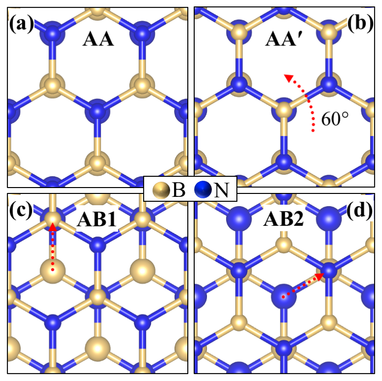
Layers of h-BN can be stacked in different ways, resulting in different material properties (Qi and Hector, 2007; Marom et al., 2010; Constantinescu et al., 2013; Gilbert et al., 2019). The AA stacking [\FigrefStackings(a)] is a trivial stacking sequence with no in-plane shift or rotation between successive layers, and it has an interlayer distance of . We include this unobserved high-energy stacking sequence in our study as a reference. The most commonly synthesized stacking sequence of h-BN is the stacking [\FigrefStackings(b)], in which each layer is a rotated copy of the preceding layer, resulting in columns of alternating B and N atoms in the bulk (Alem et al., 2009). A less common stacking sequence of h-BN is the AB (Bernal) stacking, which includes no relative rotation but only a relative shift between the layers [\FigrefStackings(c,d)]. AB-h-BN is energetically very close to -h-BN (Gilbert et al., 2019), but until recently, it was only observed in rare cases (Warner et al., 2010; Khan et al., 2016; Ji et al., 2017). The procedure to reliably manufacture this stacking was recently reported (Gilbert et al., 2019), followed by several new studies on this material (Dogan et al., 2020; Yasuda et al., 2021; Stern et al., 2021; Woods et al., 2021). For a comprehensive comparison of the stacking sequences in h-BN, we refer the reader to Ref. (Gilbert et al., 2019).
An infinite sheet of single-layer h-BN is a wide-gap insulator, yet, computational investigations have revealed that its edges and pores have a diverse set of electronic and magnetic properties (Barone and Peralta, 2008; Lai et al., 2009; Mukherjee and Bhowmick, 2011; Yamijala and Pati, 2013; Deng et al., 2017; Dogan et al., 2020; Dogan and Cohen, 2020). The unpaired electrons that occupy dangling hybrid orbitals at edges and pores result in magnetism which is absent in the pristine sheet. The most commonly formed vacancies in h-BN are boron monovacancies (i.e. a single boron atom removed from the sheet), shown in \FigrefMonolayer. These vacancies can be created by a high-energy electron beam in a transmission electron microscopy (TEM) chamber. As the beam is applied for longer periods of time, the vacancies grow into larger pores in predictable ways (Alem et al., 2011; Pham et al., 2016; Gilbert et al., 2017, 2019; Dogan et al., 2020). The pores have three nitrogen-terminated zigzag edges that form an equilateral triangle. In the large pore limit, these edges approximate the edges of an infinite sheet (N-edge), which is the most common edge type in h-BN (Zobelli et al., 2007; Alem et al., 2009; Meyer et al., 2009; Kotakoski et al., 2010; Kim et al., 2011; Ryu et al., 2015; Rajan et al., 2019; Mouhoub et al., 2020), and has magnetic properties that we elucidated in a previous computational study (Dogan and Cohen, 2020). In the current study, we first investigate the spin configurations of nanopores of various sizes in single-layer h-BN and relate them to the infinite edges. We then discuss the interactions of nested/aligned pores in multilayer h-BN. In the common -h-BN, consecutive layers are rotated by with respect to each other, and triangular pores do not neatly align. In contrast, multilayer nested pores are observed in AB-h-BN with perfectly parallel edges (Gilbert et al., 2019; Dogan et al., 2020). We report the geometries and electronic structures of all basic bilayer triangular pore combinations in which the larger of the two pores is 4 u.c. in size, and generalize the bonding patterns (or lack thereof) when available.
| NT1 (3) | NT2 (0) | ||||
| Collinear | NC | NC | NC | Collinear | |
| (eV) | |||||
| ES type | metal | half-metal | magnetic SC | nonmagnetic SC | nonmagnetic SC |
| (eV) | 0 | 4.64 | 1.94 | ||
| (eV) | 0 | 0 | 1.94 | ||
We conclude this section by noting that in AB-h-BN, the two consecutive layers are inequivalent. With the same bottom layer, the top layer may be shifted in two distinct ways to construct the AB stacking, shown in \FigrefStackings(c,d) by the red arrows, which we call AB1 and AB2. In order to keep track of all nanopore combinations, we distinguish between AB1 and AB2 stackings for the rest of the study. This property of AB-h-BN clearly distinguishes it from -h-BN and was recently utilized to generate ferroelectricity in bilayer h-BN (Yasuda et al., 2021; Stern et al., 2021; Woods et al., 2021). For a more detailed discussion of this point, we refer the reader to Ref. (Dogan and Cohen, 2020).
II Methods
We conduct density functional theory (DFT) calculations within the Perdew–Burke–Ernzerhof generalized gradient approximation (PBE GGA) (Perdew and Zunger, 1981), using the QUANTUM ESPRESSO software package with norm-conserving pseudopotentials (Giannozzi et al., 2009; Hamann, 2013). The plane-wave energy cutoff for the pseudo Kohn-Sham wavefunctions used is 80 Ry. For a unit cell of h-BN, we use a Monkhorst–Pack k-point mesh to sample the Brillouin zone (Cohen et al., 1975), and choose k-point meshes accordingly for larger unit cells. A 14 Å of vacuum is placed between the copies of the 2D system along the out-of-plane direction to isolate the sheets. In order to include the interlayer van der Waals interactions, we include a Grimme-type dispersion correction (Grimme, 2006). All atomic coordinates are relaxed until the forces on all the atoms are less than Ry/ in all three Cartesian directions, where is the Bohr radius.
III Results
III.1 Nanopores in monolayer h-BN
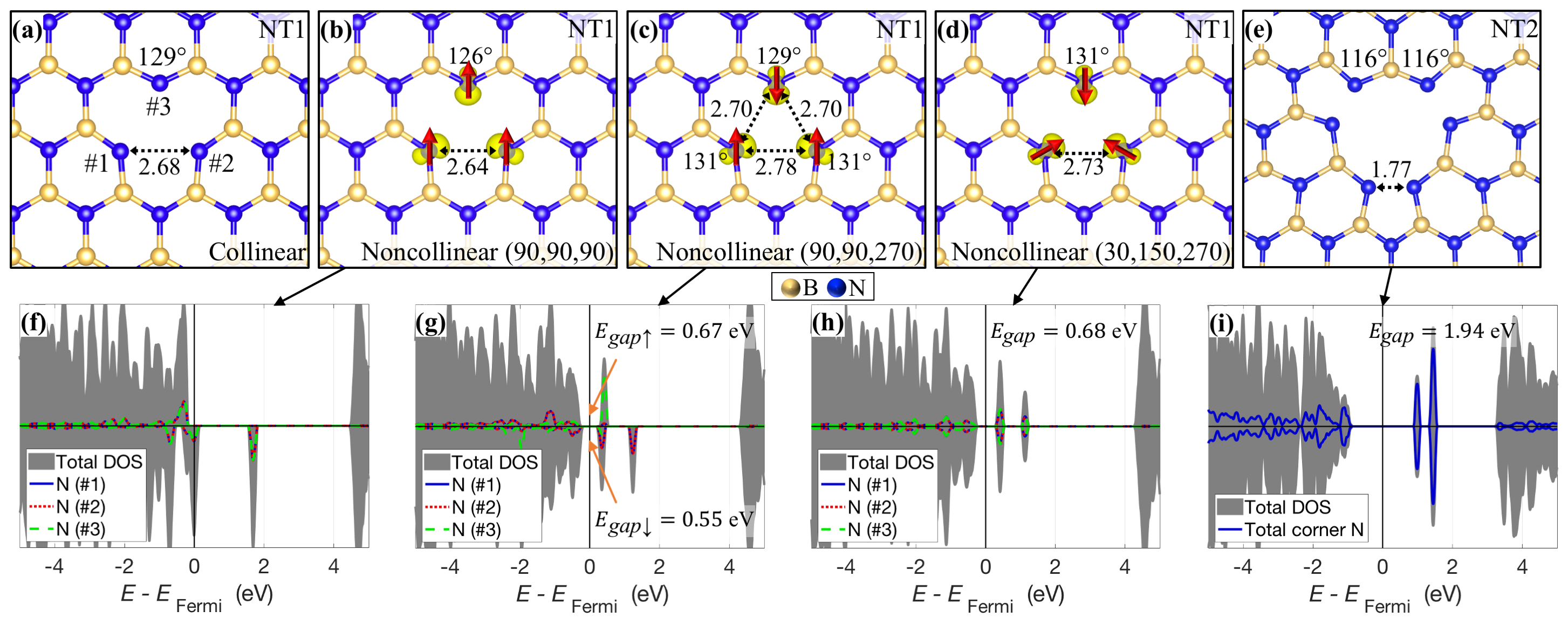
We start with a survey of the possible spin configurations in the boron monovacancy in the single layer h-BN. Throughout this article, we label pores as “NT”, where “NT” stands for “nitrogen-terminated”, and is the number of nitrogen atoms on each edge of the triangle. Thus, a boron monovacancy is denoted as NT1. In \FigrefMonolayer(a-d), we present the atomic structure of NT1 in its various magnetic configurations. \FigrefMonolayer(a) is obtained by running a collinear calculation, resulting in a structure with 3-fold symmetry. The structures in \FigrefMonolayer(b-d) are obtained by relaxing the atoms further with noncollinear spin channels and different starting configurations. All three of these configurations have lower energies compared to the collinear structure, as listed in \TabrefMLpores, and are local minima in the configuration space. We find that the 3-fold symmetric NC(30,150,270) structure has the lowest energy, but only by meV, compared to NC(90,90,270). Interestingly, the latter configuration is a triplet of atomic structures, where there are two shorter N–N distances (2.70 ) and a longer N–N distance (2.78 ). At regular temperatures (20 K 500 K), we expect both the NC(30,150,270) and NC(90,90,270) pores to be present in single layer h-BN with pores with only trace amounts of NC(90,90,90). To the best of our knowledge, previous studies have only identified NC(90,90,90) (Si and Xue, 2007; Du et al., 2009; Zhao et al., 2018; Dogan et al., 2020). Although no probing of the local magnetism of edges or pores in h-BN has been reported, ferromagnetism has been shown to occur in h-BN at room temperature (Si et al., 2014), which can be attributed to the existence of edges and pores in regular h-BN samples.
The next smallest triangular pore is NT2, which is obtained by removing three borons and one nitrogen from the system (\FigrefMonolayer(e)). In this pore, the corner nitrogens approach each other and form dimers, resulting in a collinear electronic structure ( everywhere), as reported previously (Du et al., 2009; Dogan et al., 2020).
Looking at the electronic structures of the NT1 pores (\FigrefMonolayer(f-h)), we observe that the NC(90,90,90) pore is a half-metal, i.e. the majority spin channel is insulating and the minority spin channel is a metal, the NC(90,90,270) pore is a magnetic semiconductor and the NC(30,150,270) pore is a nonmagnetic semiconductor, although the electronic structures of the latter two configurations are very similar. The antiferromagnetic state is a semiconductor with a gap of 0.51 eV. Because the spin configuration and the electronic structure are closely linked, these pores may be useful in various spintronics applications (Prinz, 1998; Wolf et al., 2001; Žutić et al., 2004; Awschalom and Flatté, 2007; Felser et al., 2007; Yazyev, 2010; Awschalom et al., 2013; Ahn, 2020). As seen in \FigrefMonolayer(i), the electronic structure of the NT2 pore is a nonmagnetic semiconductor with a larger gap (\TabrefMLpores). We present the atomic and electronic structures of larger pores in single layer h-BN (NT3–NT8) in Figures S1–S6. The key information for these larger pores is summarized in \TabrefMLsize. In each case, we fully relax the pore in a collinear calculation, and then run a self-consistent field calculation with two initial spin configurations: where all the edge spins are set as parallel (P), and where consecutive edge spins are set as antiparallel (AP). We note that we have confirmed in a few test cases that in these larger pores, further relaxations with noncollinearity cause negligible changes in atomic positions. In Figures S1–S6, the magnetization in the real space is only plotted for the P configurations (the AP configurations have equivalent plots with alternating sign). In \TabrefMLsize, we also include the case of the N-edge taken from Ref. (Dogan and Cohen, 2020), which may be interpreted as the limiting case NT.
From the results in Figures S1–S6 and \TabrefMLsize, we make a few observations: (i) The corner N atoms remain dimerized in these larger pores and thus have no magnetic moment. This causes the sequence of the absolute value of the magnetic moments to be approximately 3, 0, 3, 6, for the NT1, NT2, NT3, NT4, pores. (ii) For the NT pores with , the energy differences between P and AP spin configurations is smaller compared to NT1 and the N-edge. The comparison with NT1 can be explained by the isolation provided by the dimerized corner N atoms. The comparison with the N-edge may be due to the fact that these pores are still small, and many of the edge N atoms lack nearest and next-nearest neighbors to interact with, as opposed to the infinite edges (we know that both nearest and next-nearest neighbor interactions are important for the spin dynamics in this system, cf. (Dogan and Cohen, 2020)). This near degeneracy of different spin configurations would be advantageous in applications that rely on magnetic switching. (iii) The P configurations are consistently half-metals, and the AP configurations are either magnetic semiconductors (MSC) or nonmagnetic semiconductors (NMSC), depending on the number of available magnetic sites (written in parentheses in the first row of \TabrefMLpores and the first column of \TabrefMLsize). The band gap of the NMSC configurations gradually increases with the pore size, approaching the value of the N-edge (0.51 eV). (iv) The positions of the in-gap states for the AP configurations depend on the pore size. Because the pore size can be controlled by the duration of the applied electron beam (Pham et al., 2016; Gilbert et al., 2017), it should be possible to engineer the desired in-gap states at a desired location on the h-BN layer.
| (eV) | ES type | (eV) | ||
|---|---|---|---|---|
| NT3 (3) | P | half-metal | ||
| AP | MSC | |||
| NT4 (6) | P | half-metal | ||
| AP | NMSC | |||
| NT5 (9) | P | half-metal | ||
| AP | MSC | |||
| NT6 (12) | P | half-metal | ||
| AP | NMSC | |||
| NT7 (15) | P | half-metal | ||
| AP | MSC | |||
| NT8 (18) | P | half-metal | ||
| AP | NMSC | |||
| N-edge (Dogan and Cohen, 2020) | P | half-metal | ||
| AP | NMSC |
III.2 Nanopores in bilayer h-BN
When nanopores are created on multilayer h-BN, they tend to begin on the top layer and then propagate into the layers underneath (Gilbert et al., 2017; Dogan et al., 2020). As a first step in understanding nanopores in multilayer systems, we present results on nanopores on the top layer of bilayer h-BN, where the bottom layer remains as a full sheet. In Figures S7–S22, we present the atomic and electronic structures of pores NT1–NT4 in a single sheet stacked on a full sheet using AA, , AB1 and AB2 stacking sequences. For NT1, NT3 and NT4 pores, parallel (P) and antiparallel (AP) spin configurations are run without further relaxation of the atomic positions (NT2 remains fully spin-unplorazied), and the magnetization in the real space is only plotted for the P configurations (the AP configurations have equivalent plots with alternating sign). Our findings are also summarized in \TabrefMLporeBL. In general, the behavior of the pores in the bilayer remains very similar to their behavior in single h-BN sheets, although the small shifts in the energy levels. However, the magnetized regions around the edge N atoms do not lie entirely parallel to the sheet for the larger pores (NT3 and up), instead, these spin-polarized dangling orbitals point away from the bottom sheet by an angle , which is listed for each case in the table.
| AA | AB1 | AB2 | |||||||||||
| (eV) | (eV) | ||||||||||||
| NT1 (3) | P | ||||||||||||
| AP | |||||||||||||
| NT2 (0) | Collinear | 1.75 | n/a | 1.82 | n/a | 1.71 | n/a | 1.86 | n/a | ||||
| NT3 (3) | P | ||||||||||||
| AP | |||||||||||||
| NT4 (6) | P | ||||||||||||
| AP | |||||||||||||
Once a nanopore begins to form in the top layer of multilayer h-BN, the second layer becomes exposed the electron beam, giving rise to progressively larger and deeper (in terms of the number of layers) pores (Gilbert et al., 2017; Dogan et al., 2020). In the next part of our work, we investigate the coexistence of small pores in both layers of bilayer h-BN in order to elucidate the early stages of this process. In Figures S23–S24, we present the NT1 pores on both layers of bilayer h-BN (in this case, AB2 stacking is identical to AB1 so it is not presented separately). The NT1 & NT1 configurations are uncoupled in the sense that the pores in the neighboring layers do not interact beyond the already present van der Waals forces. We note here that for the NT1 & NT1 configurations, we have checked for potential interlayer coupling of spins by running a comprehensive collection of spin polarization combinations. We have not found a noteworthy difference in energies beyond a simple summation of the energies of spin configurations in each layer.
As the next step in the process for the AB stacking, we remove the 3 N atoms of the bottom layer that are exposed in addition to the 1N atom on the top layer. This results in the configuration in Figure S25, which is an unusual defect structure where three B atoms in the bottom layer move inward within the plane and form a trimer. This magnetic semiconductor has the band gaps eV in the two spin channels. We note that this structure is not an artifact of symmetry and seems to be robust with respect to atomic position perturbations.
For larger pores in bilayer h-BN, we focus on the AB stacking. As discussed above, due to the relative rotation between consecutive layers in the stacking, multilayer pores become irregularly shaped, whereas the AB stacking allows for nested and aligned pores (Dogan et al., 2020). As the next step in AB1-h-BN, we assume that the NT2 pore has formed in the top layer, and then we remove the boron in the center of the exposed area in the bottom layer (cf. Figure S13). This results in the NT2 & NT1 structure presented in Figure S26, which is also a uncoupled structure (half-metal, eV). Removing the 6 exposed nitrogens from this configuration results in our first coupled structure, presented in \FigrefBLpores_1(a). This 3-fold symmetric structure is a magnetic semiconductor which has 6 interlayer B–N bonds. Forming the NT2 & NT1 structure in AB2-h-BN is possible in two different ways by removing a boron from either the center or the corner of the exposed area in the bottom layer (cf. Figure S14). In both cases, we get uncoupled structures that are presented in Figures S27–S28 (both magnetic semiconductors with the band gaps eV and eV, respectively). Finally, we present the NT2 & NT2 structures in the AA and AB1 stacking sequences in Figures S29–S30, both of which are uncoupled and nonmagnetic semiconductors with the band gaps eV and eV, respectively (AB2 is equivalent to AB1).
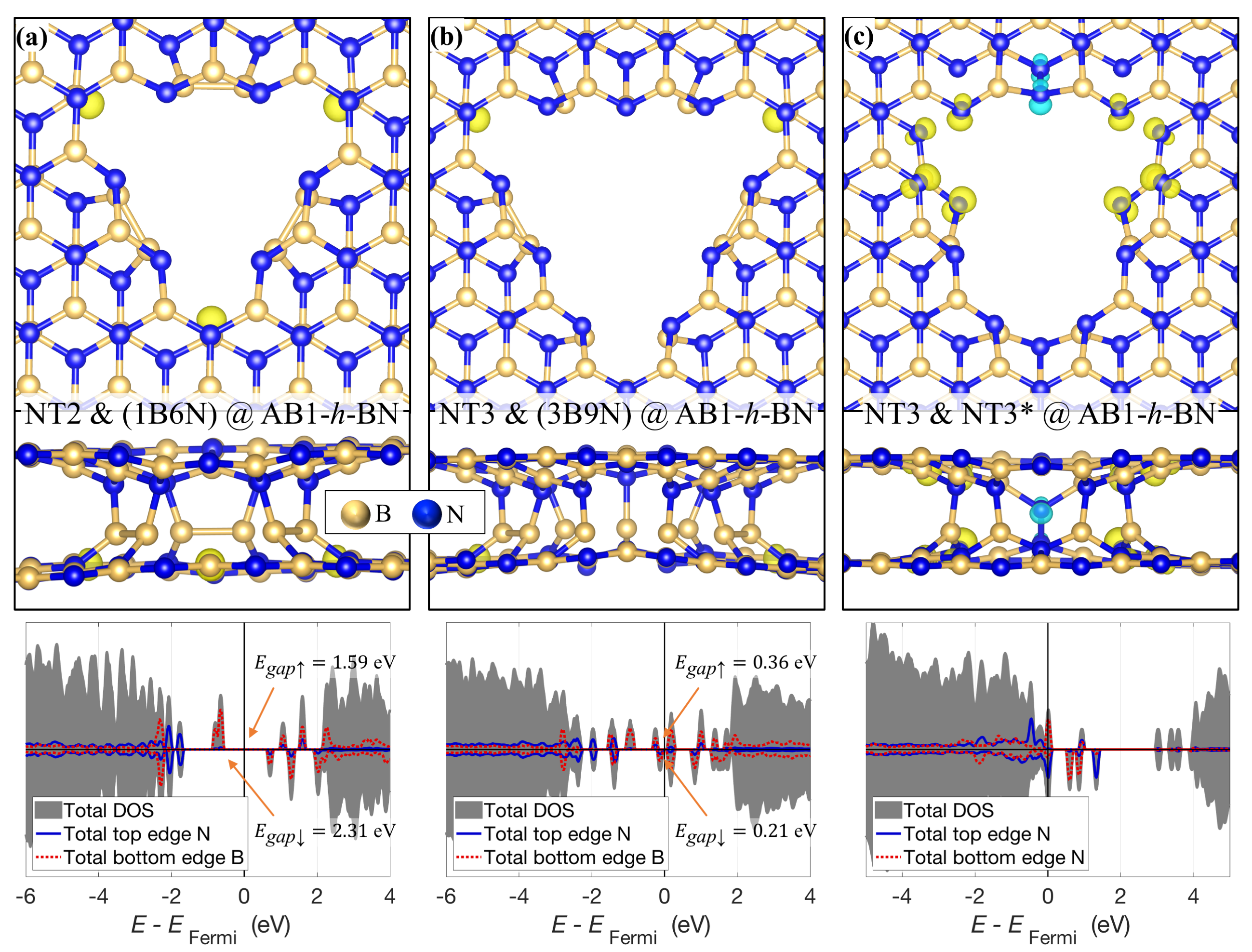
We then move to the NT3 pore in the top layer of AB1-h-BN. Removing one of the three exposed borons in the bottom layer (cf. Figure S17) results in the NT3 & NT1 uncoupled structure (Figure S31), which is a half-metal with eV. Similarly, the NT3 & NT2 structure in AB1-h-BN is also uncoupled (Figure S32) but metallic. Next, we remove the remaining exposed nitrogens so that all the atoms in the bottom layer that are exposed when the top layer has an NT3 pore are removed. This results in the structure in \FigrefBLpores_1(b) which has reflection symmetry and 9 interlayer B–N bonds, and is a magnetic semiconductor. An interesting effect occurs when the NT3 & NT3 structure in AB1-h-BN is set up and relaxed, in which two edge nitrogens in the bottom layer detach from their neighbors and form an molecule. When the molecule is taken out of the system, the resulting coupled structure, which is metallic, is presented in \FigrefBLpores_1(c). Because the bottom layer has lost two nitrogens, we call this configuration NT3 & NT3*, and it has 4 interlayer B–N bonds as well as 1 interlayer N–N bond. This structure demonstrates that not all nested NT & NT pores are possible in their expected stoichiometry in bilayer and therefore multilayer AB-h-BN.
There are three inequivalent NT3 & NT1 structures in AB2-h-BN depending on which boron in the bottom layer is removed (cf. Figure S18). These three result in uncoupled half-metallic structures that are presented in Figures S33–S35 with eV, respectively. The two inequivalent NT3 & NT2 structures in AB2-h-BN are also uncoupled and half-metallic, and presented in Figures S36–S37 ( eV, respectively). The NT3 & NT3 structure in AB2-h-BN is equivalent to that in AB1-h-BN (\FigrefBLpores_1(c)). Finally, we present the NT3 & NT3 structure in the AA stacking sequence in Figure S38, which is a magnetic metal with interlayer bonding of the mid-edge nitrogens.
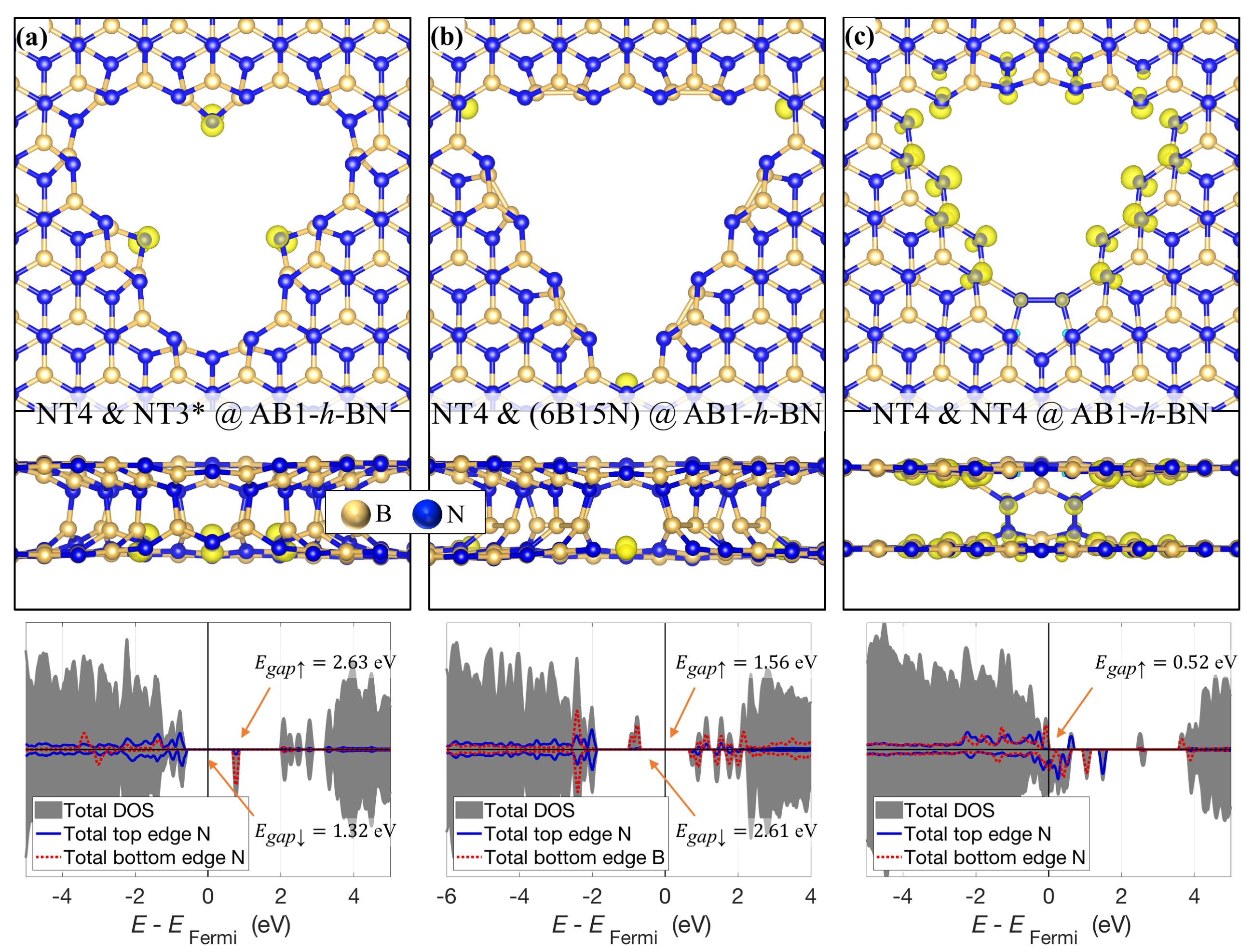
The largest size we have considered for bilayer h-BN in this study is the NT4 pore. We start with the NT4 & NT1 configuration in AB1-h-BN of which there are two (Figures S39–S40). Both of these are uncoupled and half-metallic with eV, respectively. When the bottom layer has an NT2 pore, interlayer bonds form, but not all the top edge nitrogens are bonded. This coupled configuration (NT4 & NT2) is presented in Figure S41 and is a half-metal with eV. Enlarging the bottom layer pore one more step to set up the NT4 & NT3 structure results in the detachment of three molecules and 12 interlayer B–N bonds (\FigrefBLpores_2(a)). By losing most of its dangling orbitals, this system, which we call NT4 & NT3*, becomes a fairly large-gap magnetic semiconductor. Next, we remove the remaining exposed nitrogens from this configuration so that all the atoms in the bottom layer that are exposed when the top layer has an NT4 pore are removed. This results in the structure in \FigrefBLpores_2(b) which has 12 interlayer B–N bonds and is a magnetic semiconductor. The NT4 & NT4 bilayer pore in AB1-h-BN also results in some interlayer bonding(\FigrefBLpores_2(c)). In this configuration, the alignment of the two edges (diagonal in \FigrefBLpores_2(b)) is different from the alignment of the remaining edge (horizontal in \FigrefBLpores_2(c). The interlayer bonds form only at the latter edge. These two edge types correspond to the infinite edges in Figures 5 and 6 of (Dogan and Cohen, 2020), respectively. This particular pattern of interlayer bonding should hold for all NT & NT pores () of AB-h-BN, where interlayer N–N bonds occur only at one of the edges.
In AB2-h-BN, there are four inequivalent NT4 & NT1 structures depending on which boron in the bottom layer is removed (cf. Figure S22). These structures are presented in Figures S42–S45. The NT4 & NT1 (1) structure has a single interlayer N–N bond and is a magnetic metal. The NT4 & NT1 (2) structure has two interlayer N–N bonds and is a magnetic half-metal with eV. The remaining two NT4 & NT1 structures are uncoupled half-metals with eV, respectively. The three inequivalent NT4 & NT2 structures are presented in Figures S46–S48. These structures are uncoupled half-metals with eV, respectively. Among the two inequivalent NT4 & NT3 configurations, the first one (Figure S49) has 2 interlayer N–N bonds and is a magnetic metal. This bonding pattern should hold for all NT & NT pores () of AB-h-BN, where interlayer N–N bonds each occur at two of the edges. The second NT4 & NT3 configuration in AB2-h-BN (Figure S50) is an uncoupled structure that is a half-metal with eV. The NT4 & NT4 structure in AB2-h-BN is equivalent to that in AB1-h-BN (\FigrefBLpores_2(c)). Finally, the NT4 & NT4 structure in the AA stacking sequence is presented in Figure S51, which is a magnetic half-metal ( eV) with interlayer bonding of the two mid-edge nitrogens on each edge.
IV Conclusion
We conducted a first-principles study of the nitrogen-terminated triangular nanopores in h-BN with a special focus on Bernal-stacked h-BN (AB-h-BN). We found that the ground state of the smallest pore (B monovacancy) is a 3-fold symmetric configuration with zero total magnetization. However, the existence of magnetic configurations that are almost degenerate with the ground state heightens the potential of magnetic switchability. For larger pores in single-layer h-BN, configurations with parallel and antiparallel neighboring magnetizations are also close in energy, indicating the likelihood of easier magnetization of these pores compared to longer edges where energy differences are larger. For bilayer configurations with pores in both layers, we find that in most cases, the layers remain uncoupled, i.e., no significant out-of-plane movement or bonding occurs. However, several structures that are expected to occur during electron irradiation do form interlayer bonds, reducing the magnetic character of the pores. We expect these types of coupled structures to occur during electron irradiation alongside the simpler decoupled structures. We also find that some nested pores are not possible in their expected stoichiometry in bilayer and therefore multilayer AB-h-BN as a result of to the detachment of nitrogens by forming molecules. We hope that our results will motivate experimental studies that closely investigate the magnetic and electronic properties of these pores in h-BN, given their enormous potential in applications such as DNA sequencing.
Acknowledgments
This work was supported by the Director, Office of Science, Office of Basic Energy Sciences, Materials Sciences and Engineering Division, of the U.S. Department of Energy under contract No. DE-AC02-05-CH11231, within the Theory of Materials program (KC2301), which supported first-principles computations of the atomic structures. Further support for theoretical work was provided by the NSF Grant No. DMR-1926004 which supported first-principles computations of the precise electronic structures. Computational resources used were Cori at National Energy Research Scientific Computing Center (NERSC), which is supported by the Office of Science of the US Department of Energy under contract no. DE-AC02-05-CH11231, Stampede2 at the Texas Advanced Computing Center (TACC) through Extreme Science and Engineering Discovery Environment (XSEDE), which is supported by National Science Foundation (NSF) under grant no. ACI-1053575, Frontera at TACC, which is supported by NSF grant no. OAC-1818253, and Bridges-2 at the Pittsburgh Supercomputing Center (PSC), which is supported by NSF award number ACI-1928147.
References
- Koenig et al. (2012) S. P. Koenig, L. Wang, J. Pellegrino, and J. S. Bunch, Nature Nanotechnology 7, 728 (2012).
- Choi et al. (2016) S. Choi, T. T. Tran, C. Elbadawi, C. Lobo, X. Wang, S. Juodkazis, G. Seniutinas, M. Toth, and I. Aharonovich, ACS Applied Materials & Interfaces 8, 29642 (2016).
- Zhao et al. (2019) J. Zhao, G. He, S. Huang, L. F. Villalobos, M. Dakhchoune, H. Bassas, and K. V. Agrawal, Science Advances 5, eaav1851 (2019).
- Caldwell et al. (2019) J. D. Caldwell, I. Aharonovich, G. Cassabois, J. H. Edgar, B. Gil, and D. N. Basov, Nature Reviews Materials 4, 552 (2019), number: 8 Publisher: Nature Publishing Group.
- Liu et al. (2021) H. Liu, C. Y. You, J. Li, P. R. Galligan, J. You, Z. Liu, Y. Cai, and Z. Luo, Nano Materials Science 3, 291 (2021).
- Song et al. (2021) S.-B. Song, S. Yoon, S. Y. Kim, S. Yang, S.-Y. Seo, S. Cha, H.-W. Jeong, K. Watanabe, T. Taniguchi, G.-H. Lee, J. S. Kim, M.-H. Jo, and J. Kim, Nature Communications 12, 7134 (2021), number: 1 Publisher: Nature Publishing Group.
- Liu et al. (2013) S. Liu, B. Lu, Q. Zhao, J. Li, T. Gao, Y. Chen, Y. Zhang, Z. Liu, Z. Fan, F. Yang, L. You, and D. Yu, Advanced Materials 25, 4549 (2013).
- Zhou et al. (2013) Z. Zhou, Y. Hu, H. Wang, Z. Xu, W. Wang, X. Bai, X. Shan, and X. Lu, Scientific Reports 3, 3287 (2013).
- Muthukumar et al. (2015) M. Muthukumar, C. Plesa, and C. Dekker, Physics Today 68, 40 (2015), publisher: American Institute of Physics.
- Heerema and Dekker (2016) S. J. Heerema and C. Dekker, Nature Nanotechnology 11, 127 (2016).
- Deamer et al. (2016) D. Deamer, M. Akeson, and D. Branton, Nature Biotechnology 34, 518 (2016).
- Dogan and Cohen (2020) M. Dogan and M. L. Cohen, Physical Review B 102, 155419 (2020), publisher: American Physical Society.
- Qi and Hector (2007) Y. Qi and L. G. Hector, Applied Physics Letters 90, 081922 (2007).
- Marom et al. (2010) N. Marom, J. Bernstein, J. Garel, A. Tkatchenko, E. Joselevich, L. Kronik, and O. Hod, Physical Review Letters 105, 046801 (2010).
- Constantinescu et al. (2013) G. Constantinescu, A. Kuc, and T. Heine, Physical Review Letters 111, 036104 (2013).
- Gilbert et al. (2019) S. M. Gilbert, T. Pham, M. Dogan, S. Oh, B. Shevitski, G. Schumm, S. Liu, P. Ercius, S. Aloni, M. L. Cohen, and A. Zettl, 2D Materials 6, 021006 (2019).
- Alem et al. (2009) N. Alem, R. Erni, C. Kisielowski, M. D. Rossell, W. Gannett, and A. Zettl, Physical Review B 80, 155425 (2009).
- Warner et al. (2010) J. H. Warner, M. H. Rümmeli, A. Bachmatiuk, and B. Büchner, ACS Nano 4, 1299 (2010).
- Khan et al. (2016) M. H. Khan, G. Casillas, D. R. G. Mitchell, H. K. Liu, L. Jiang, and Z. Huang, Nanoscale 8, 15926 (2016).
- Ji et al. (2017) Y. Ji, B. Calderon, Y. Han, P. Cueva, N. R. Jungwirth, H. A. Alsalman, J. Hwang, G. D. Fuchs, D. A. Muller, and M. G. Spencer, ACS Nano 11, 12057 (2017).
- Dogan et al. (2020) M. Dogan, S. M. Gilbert, T. Pham, B. Shevitski, P. Ercius, S. Aloni, A. Zettl, and M. L. Cohen, Applied Physics Letters 117, 023102 (2020), publisher: AIP Publishing LLC AIP Publishing.
- Yasuda et al. (2021) K. Yasuda, X. Wang, K. Watanabe, T. Taniguchi, and P. Jarillo-Herrero, Science 372, 1458 (2021), publisher: American Association for the Advancement of Science Section: Report.
- Stern et al. (2021) M. V. Stern, Y. Waschitz, W. Cao, I. Nevo, K. Watanabe, T. Taniguchi, E. Sela, M. Urbakh, O. Hod, and M. B. Shalom, Science 372, 1462 (2021), publisher: American Association for the Advancement of Science Section: Report.
- Woods et al. (2021) C. R. Woods, P. Ares, H. Nevison-Andrews, M. J. Holwill, R. Fabregas, F. Guinea, A. K. Geim, K. S. Novoselov, N. R. Walet, and L. Fumagalli, Nature Communications 12, 347 (2021).
- Barone and Peralta (2008) V. Barone and J. E. Peralta, Nano Letters 8, 2210 (2008).
- Lai et al. (2009) L. Lai, J. Lu, L. Wang, G. Luo, J. Zhou, R. Qin, Z. Gao, and W. N. Mei, The Journal of Physical Chemistry C 113, 2273 (2009).
- Mukherjee and Bhowmick (2011) R. Mukherjee and S. Bhowmick, Journal of Chemical Theory and Computation 7, 720 (2011).
- Yamijala and Pati (2013) S. S. Yamijala and S. K. Pati, The Journal of Physical Chemistry C 117, 3580 (2013).
- Deng et al. (2017) J. Deng, Y. Yin, H. Niu, X. Ding, J. Sun, and N. V. Medhekar, Scientific Reports 7, 7855 (2017).
- Alem et al. (2011) N. Alem, R. Erni, C. Kisielowski, M. D. Rossell, P. Hartel, B. Jiang, W. Gannett, and A. Zettl, Physica Status Solidi – Rapid Research Letters 5, 295 (2011).
- Pham et al. (2016) T. Pham, A. L. Gibb, Z. Li, S. M. Gilbert, C. Song, S. G. Louie, and A. Zettl, Nano Letters 16, 7142 (2016).
- Gilbert et al. (2017) S. M. Gilbert, G. Dunn, A. Azizi, T. Pham, B. Shevitski, E. Dimitrov, S. Liu, S. Aloni, and A. Zettl, Scientific Reports 7, 15096 (2017).
- Zobelli et al. (2007) A. Zobelli, A. Gloter, C. P. Ewels, G. Seifert, and C. Colliex, Physical Review B 75, 245402 (2007).
- Meyer et al. (2009) J. C. Meyer, A. Chuvilin, G. Algara-Siller, J. Biskupek, and U. Kaiser, Nano Letters 9, 2683 (2009).
- Kotakoski et al. (2010) J. Kotakoski, C. H. Jin, O. Lehtinen, K. Suenaga, and A. V. Krasheninnikov, Physical Review B 82, 113404 (2010).
- Kim et al. (2011) J. S. Kim, K. B. Borisenko, V. Nicolosi, and A. I. Kirkland, ACS Nano 5, 3977 (2011), publisher: American Chemical Society.
- Ryu et al. (2015) G. H. Ryu, H. J. Park, J. Ryou, J. Park, J. Lee, G. Kim, H. S. Shin, C. W. Bielawski, R. S. Ruoff, S. Hong, and Z. Lee, Nanoscale 7, 10600 (2015).
- Rajan et al. (2019) A. G. Rajan, K. S. Silmore, J. Swett, A. W. Robertson, J. H. Warner, D. Blankschtein, and M. S. Strano, Nature Materials 18, 129 (2019), number: 2 Publisher: Nature Publishing Group.
- Mouhoub et al. (2020) O. Mouhoub, R. Martinez-Gordillo, J. Nelayah, G. Wang, J.-H. Park, K. K. Kim, Y. H. Lee, C. Bichara, A. Loiseau, C. Ricolleau, H. Amara, and D. Alloyeau, Physical Review Materials 4, 014005 (2020), publisher: American Physical Society.
- Perdew and Zunger (1981) J. P. Perdew and A. Zunger, Physical Review B 23, 5048 (1981).
- Giannozzi et al. (2009) P. Giannozzi, S. Baroni, N. Bonini, M. Calandra, R. Car, C. Cavazzoni, Davide Ceresoli, G. L. Chiarotti, M. Cococcioni, I. Dabo, A. D. Corso, S. d. Gironcoli, S. Fabris, G. Fratesi, R. Gebauer, U. Gerstmann, C. Gougoussis, Anton Kokalj, M. Lazzeri, L. Martin-Samos, N. Marzari, F. Mauri, R. Mazzarello, Stefano Paolini, A. Pasquarello, L. Paulatto, C. Sbraccia, S. Scandolo, G. Sclauzero, A. P. Seitsonen, A. Smogunov, P. Umari, and R. M. Wentzcovitch, Journal of Physics: Condensed Matter 21, 395502 (2009).
- Hamann (2013) D. R. Hamann, Physical Review B 88, 085117 (2013).
- Cohen et al. (1975) M. L. Cohen, M. Schlüter, J. R. Chelikowsky, and S. G. Louie, Physical Review B 12, 5575 (1975).
- Grimme (2006) S. Grimme, Journal of Computational Chemistry 27, 1787 (2006).
- Si and Xue (2007) M. S. Si and D. S. Xue, Physical Review B 75, 193409 (2007).
- Du et al. (2009) A. Du, Y. Chen, Z. Zhu, R. Amal, G. Q. M. Lu, and S. C. Smith, Journal of the American Chemical Society 131, 17354 (2009).
- Zhao et al. (2018) L.-S. Zhao, C.-P. Chen, L.-L. Liu, H.-X. Yu, Y. Chen, and X.-C. Wang, Chinese Physics B 27, 016301 (2018).
- Si et al. (2014) M. S. Si, D. Gao, D. Yang, Y. Peng, Z. Y. Zhang, D. Xue, Y. Liu, X. Deng, and G. P. Zhang, The Journal of Chemical Physics 140, 204701 (2014).
- Prinz (1998) G. A. Prinz, Science 282, 1660 (1998), publisher: American Association for the Advancement of Science Section: Review.
- Wolf et al. (2001) S. A. Wolf, D. D. Awschalom, R. A. Buhrman, J. M. Daughton, S. v. Molnár, M. L. Roukes, A. Y. Chtchelkanova, and D. M. Treger, Science 294, 1488 (2001), publisher: American Association for the Advancement of Science Section: Special Reviews.
- Žutić et al. (2004) I. Žutić, J. Fabian, and S. Das Sarma, Reviews of Modern Physics 76, 323 (2004), publisher: American Physical Society.
- Awschalom and Flatté (2007) D. D. Awschalom and M. E. Flatté, Nature Physics 3, 153 (2007), number: 3 Publisher: Nature Publishing Group.
- Felser et al. (2007) C. Felser, G. H. Fecher, and B. Balke, Angewandte Chemie International Edition 46, 668 (2007).
- Yazyev (2010) O. V. Yazyev, Reports on Progress in Physics 73, 056501 (2010), publisher: IOP Publishing.
- Awschalom et al. (2013) D. D. Awschalom, L. C. Bassett, A. S. Dzurak, E. L. Hu, and J. R. Petta, Science 339, 1174 (2013), publisher: American Association for the Advancement of Science Section: Review.
- Ahn (2020) E. C. Ahn, npj 2D Materials and Applications 4, 1 (2020), number: 1 Publisher: Nature Publishing Group.