Ab initio study on the atomic and electronic structures of twisted InSe bilayer
Abstract
The electronic properties of the twisted InSe bilayer are studied by large-scale density functional theory. Spectral Function Unfolding reveals that the electronic structure of the twisted system can be described in terms of a combination of features of the bandstructures of the aligned InSe bilayer with different stacking configurations, enabling predictions of the band gap and the effective mass for holes. The effective mass for holes in the twisted InSe bilayer is shown to be influenced primarily by the interlayer distance. The intralayer and interlayer exciton binding energies are thus calculated based on a model recently developed by Ruiz-Tijerina et al. We apply similar analysis to the trilayer heterostructure InSe/hBN/InSe: its electronic structure is shown to be well-described by the superposition of band structures of two InSe monolayers with a small coupling through the hBN layer.
E-mail: n.d.m.hine@warwick.ac.uk
Keywords : InSe, twistronics, effective mass for holes, band gap
1 Introduction
The ideas behind the burgeoning field of twistronics have been applied in recent years to a range of different low-dimensional materials. In twisted bilayer graphene (TBG), the intervalley coherence between electrons at the two valleys leads to a Mott insulator phase and to superconductivity [1]. Tarnopolsky et al. proposed that flat bands appear at magic angles with a periodicity of 3/2 () in TBG. They suggested that lowest Landau level in a torus is similar to the flat bands seen in TBG [2]. The Dirac electrons in twisted graphene bilayer were shown to be localised in regions corresponding to AA stacking, because of the moiré potential. Their velocities approach toward zero as the twist angle decreases to be smaller than 3∘, leading to the appearance of flat bands [3]. Lopes dos Santos et al. showed that these localised states can be found in regions other than AA stacking if the twist angle is smaller than the magic angle (1.08o) based on the continuum model [4]. The same localisation in the AA stacking for the flat band can also be seen in twisted MoS2 bilayer from a tight-binding model [5].
Furthermore, Zhan et al. have shown that ultraflat bands occur at any small twist angles in twisted transition metal dichalcogenides (TMDCs) and the localisation of the charge density becomes obvious as the twist angle decreases based on a tight-binding model. They suggested that the strongly correlated states can be well studied as the twist angle below 7o [6]. The long-period moiré pattern induced by a small twist angle in twisted TMDCs leads to the significant changes of optical absorption spectrum [7].
The anisotropic transport properties of the twisted black phosphorene bilayer can be tuned by varying the twist angle [8]. Furthermore, a spontaneous electric polarisation was seen for the same twisted system with weak interlayer coupling [8]. The interlayer coupling strength is determined by the twist angle. The band gap changes differently in strong and weak interlayer coupling systems: band gap decreases with increasing electric field for strong interlayer coupling systems, whereas there is a linear Stark effect for weak interlayer coupling systems [8]. In addition. ferroelectric-like domains were seen in the twisted hBN bilayer, both in theory and experiments, because there is a large surface potential originating from the out-of-plane B-N dipoles in the two different layers [9].
Previous studies have shown that the carrier mobility is high in few-layer InSe and the variation of the band gap is large (more than 1 eV) for different thickness of InSe. Furthermore, an indirect-direct band gap transition can be seen by tuning the thickness of InSe due to the strong interlayer coupling [10, 11, 12]. The indirect-direct band gap transition is also seen when tuning the twist angle between two InSe bilayers from 3o to 1.48o with an increase of band gap at the same time [13]. The charge density for the state at the valence band maximum (VBM) becomes more localised in the region with the smallest interlayer distance when the twist angle decreases to 1.48o. However, the charge density for the conduction band minimum (CBM) spread over the whole atomic structure [13]. Structural relaxation is important for this system because the charge density localised in the region with the largest interlayer distance without structural relaxation. The formation energies for twist angles from 1.48o to 3o are similar, suggesting that the twisted systems with twist angle from 1.48o to 3o are all possibly grown in the experiment [13].
In this work, we have studied the band structure and the projected density of states of the VBM, firstly for the InSe bilayer with different stacking configurations, and then for twisted InSe bilayer. The displacement (and residual force distribution) of each atom after geometry optimisation is also discussed. It is shown that the band structure from the primitive cell calculation can be used to describe the effective band structure of twisted InSe bilayer from the supercell calculation. The interlayer distance resulting from the different stacking configurations in twisted InSe bilayer is a major factor in terms of its influence on the band structure. Finally, the hBN-spaced twisted InSe bilayer is also introduced and discussed in this work. Its band structure is very similar to the superposition of two InSe monolayers, and also matches well with the band structure of InSe monolayer from the primitive cell calculation. This indicates that a single spacer layer of hBN is sufficient to recover essentially monolayer-like behaviour.
2 Computational Methods
The atomic and band structures of InSe bilayers with different stacking configurations were calculated within the primitive cells by Quantum Espresso simulation package [14, 15]. Scalar-relativistic ultrasoft pseudopotentials from the GBRV library [16] were used. Van der Waals (vdW) interactions were treated by adopting optB88-vdW functional [17] as the exchange-correlation functional. The optimised norm-conserving Vanderbilt pseudopotentials (fully-relativistic) [18] for GGA-PBE from PseudoDojo [19] was adopted for the calculations which considered spin-orbit coupling. The vdW correction was not considered in the calculation including spin-orbit coupling.
A large vacuum spacing of 20 Å was used to avoid spurious interaction between periodic images of the system. Calculations were performed with a 1632.7 eV cut-off energy and a 10101 Monkhorst-Pack [20] kpoint sampling grid. During the ionic minimisation process, electronic convergence was such that forces were converged to 510-5 eV/Å and the total energy tolerance for all atoms was 310-7 eV.
Calculations on the twisted bilayer system must be performed at very large length scales to enable a low lattice mismatch between the coincident supercells representing each layer. The linear-scaling density functional theory (LS-DFT) package, ONETEP [21, 22], was used to perform the calculations of the twisted InSe bilayer and InSe/hBN/InSe heterostructure in this work. The projector augmented waves (PAWs) [23, 24, 25] with the GGA-PBE potentials from the GBRV library [16] were employed. The same vdW correction functional (optB88-vdW [17]) was also adopted in this simulation package. The atomic structures with a vacuum spacing of 20 Å were calculated with a 1200 eV cut-off energy for the psinc grid and 12 a0 NGWF radius. The geometry optimisation force tolerance is 0.12 eV/Å and enthalpy tolerance is 310-5 eV/atom.
Python-based tools building on the atomic simulation environment (ASE) [26] were used to generate the atomic structures and display the distribution of force. The visualisation for electronic and structural analysis (VESTA) [27] was also used to display the atomic structures and the isosurfaces of charge densities.
Appropriately-sized supercells are found by searching for a pair of coincident supercells of each of the two layers and for which both in-plane lattice vectors of each layer match with minimal strain. One layer ( here) is subjected to a rotation of angle and, to make the match exact, a near-unitary strain tensor is applied. This produces the following equations, similar to the method described in Stradi et al: [28]:
| (1) |
where
| (2) |
and
| (3) |
for integer , , and . The finding of a supercell match proceeds by first choosing a range of in which to search, and a range of supercell size, then for each set of values of for which the determinant of the supercell matrix is in that range, the values of that most-closely match for layer are determined, then the values of and that make the match exact are found. If these are below a chosen threshold, the match is accepted, or if not, the angle is further refined until no further improvement can be obtained.
Generally, there is a trade-off between the supercell size and the magnitude of strain that must be accepted in order to make a coincident cell. The supercell size is expected to increase as the twist angle decreases ( 1/) [13]. For the supercells used in this work, the values of strain on the InSe layers are under 0.8% and those of shear are zero to numerical precision.
3 Results and Discussions
3.1 InSe bilayers with different stacking configurations
When two aligned InSe monolayers are stacked on top of each other to form a bilayer, there are five possible stacking configurations, as addressed in previous studies [29, 13]. Fig. 1 shows the top and side views of these five stacking configurations. The A-1 and A-2 belong to the category we refer to as A-type, whereas the B-1, B-2 and B-3 are B-type. A stacking configuration in either category can be transformed into any of the others in the same category by a translation.
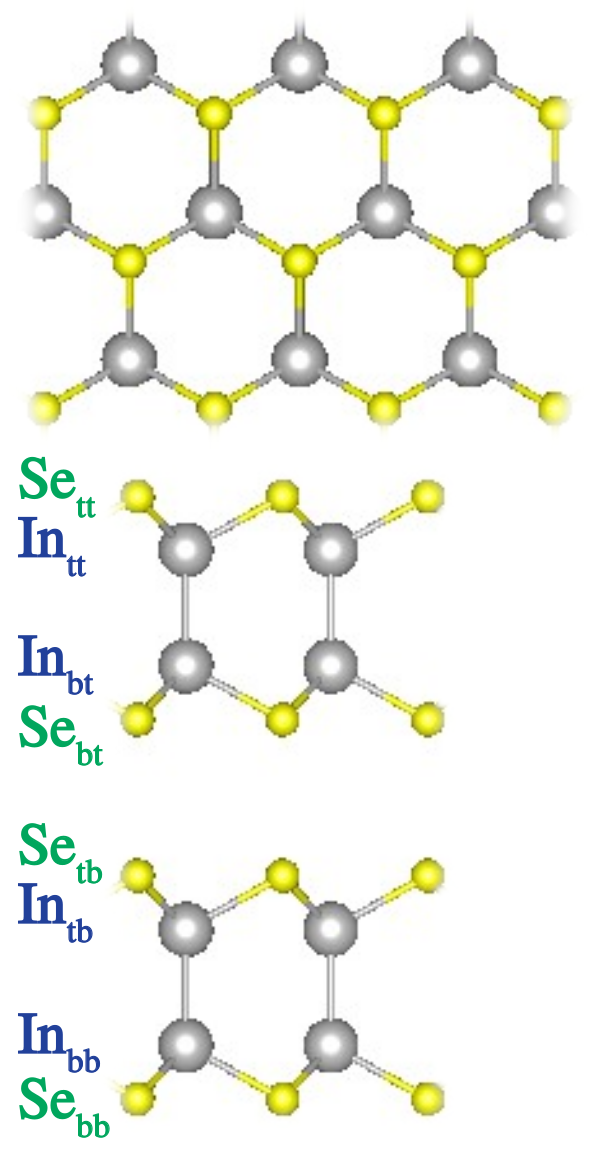
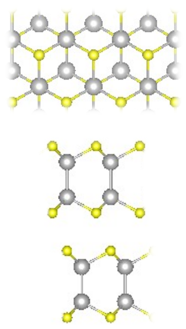
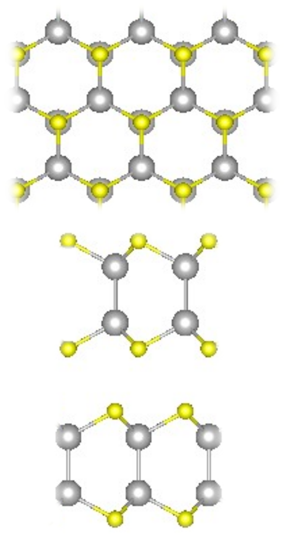
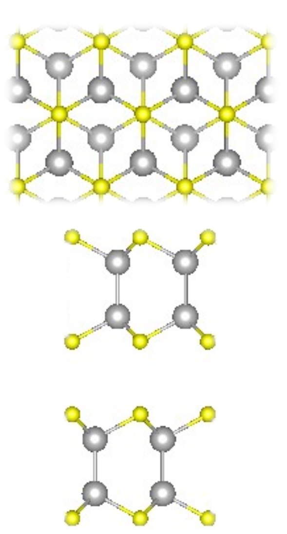
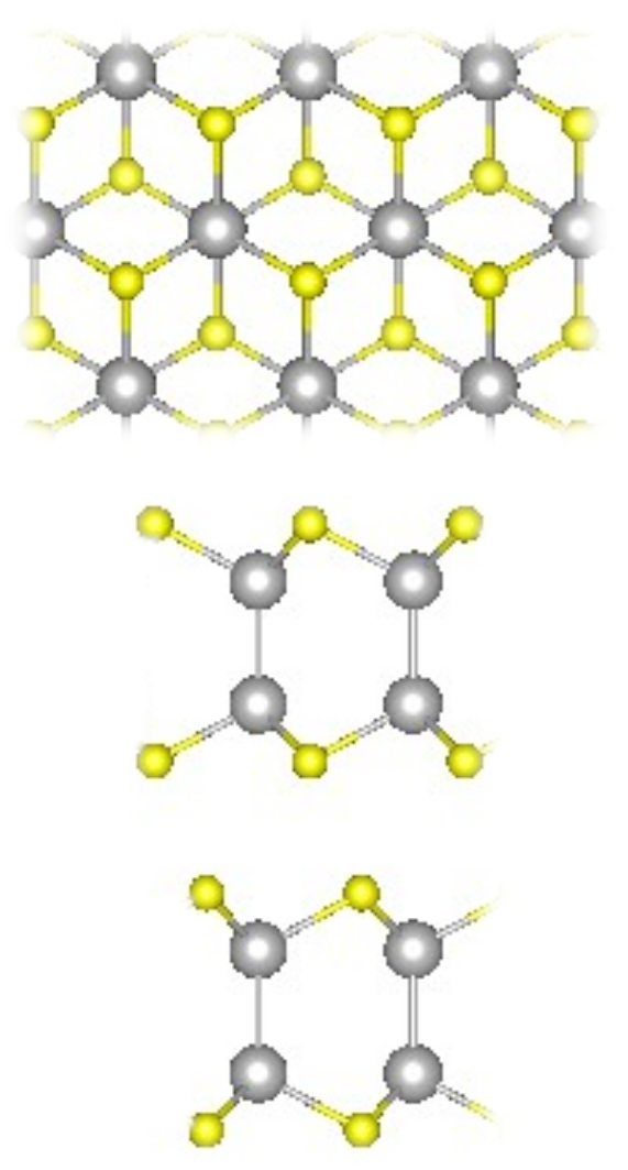
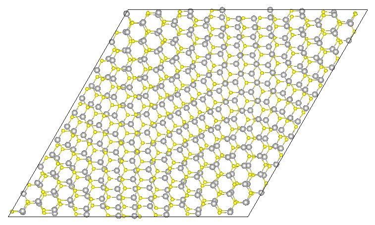
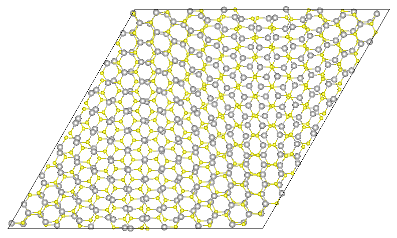
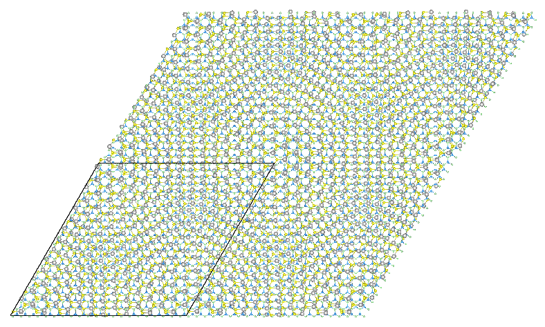
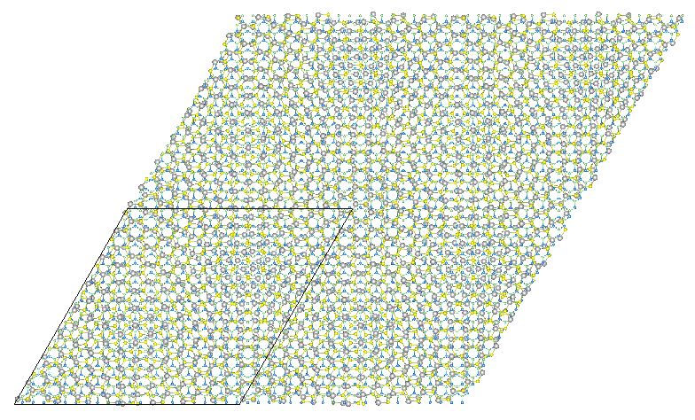
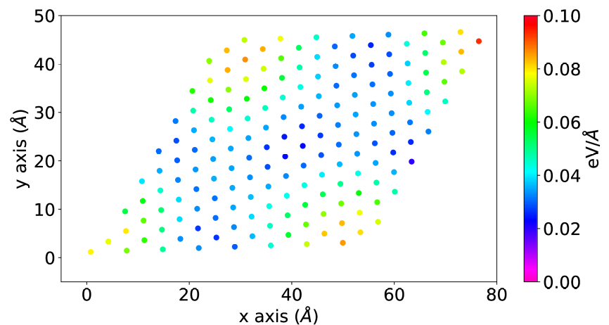
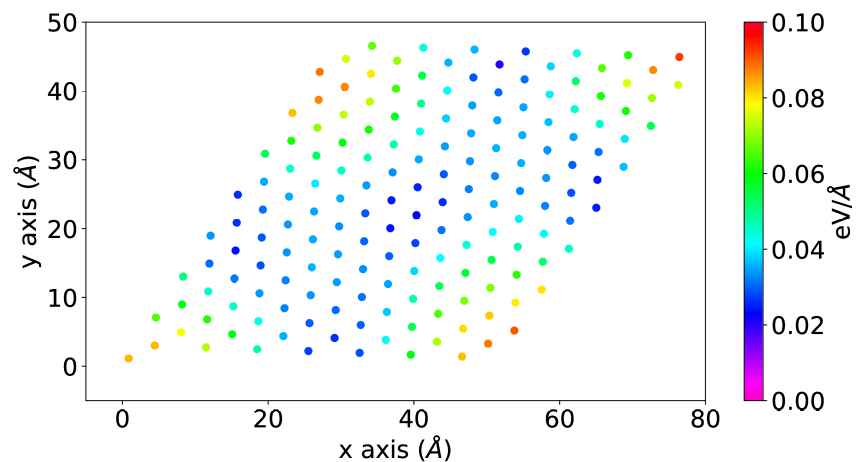
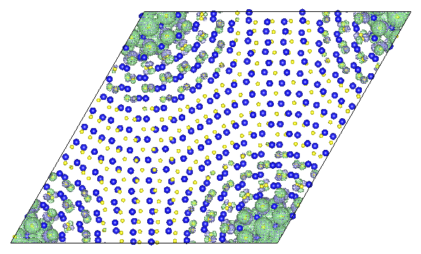
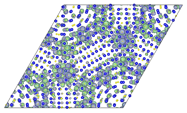
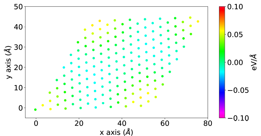
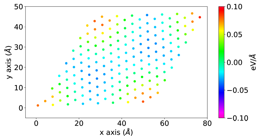
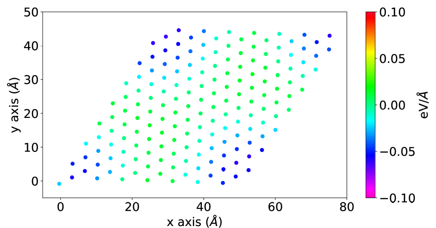
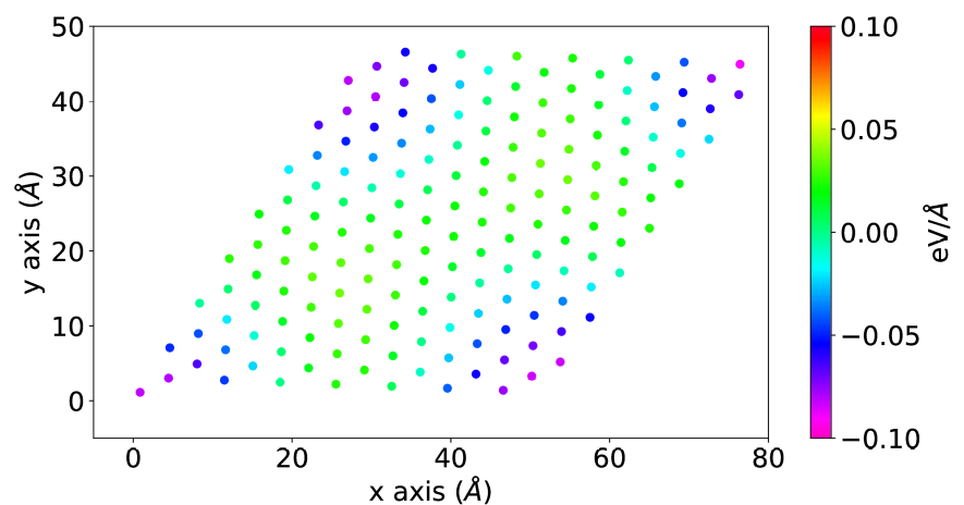
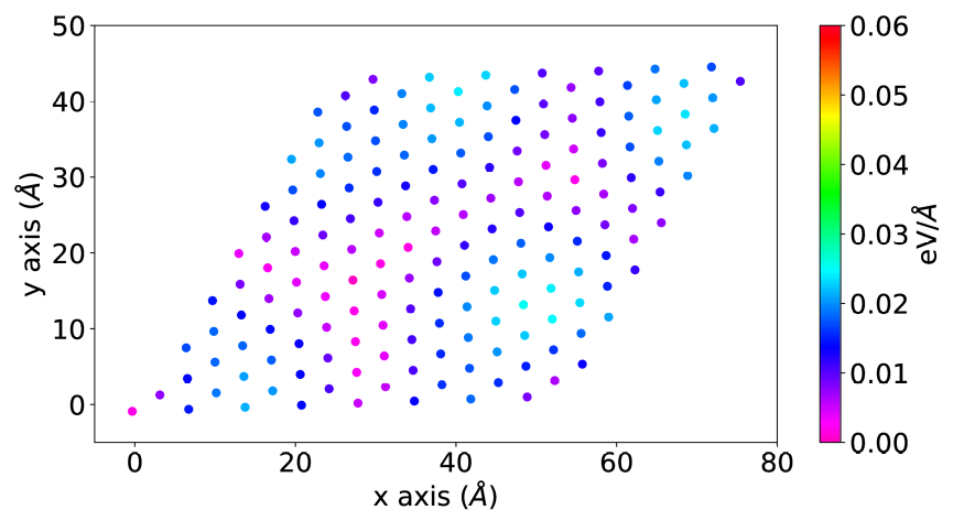
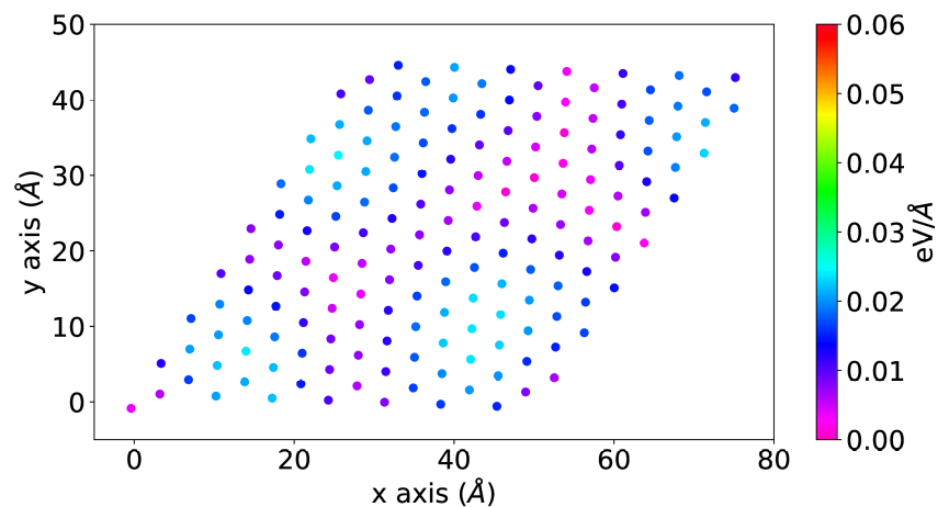
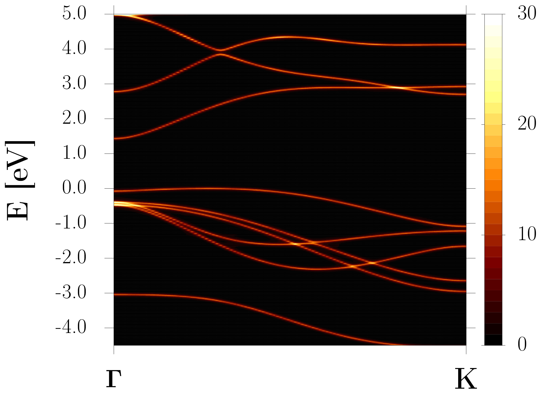
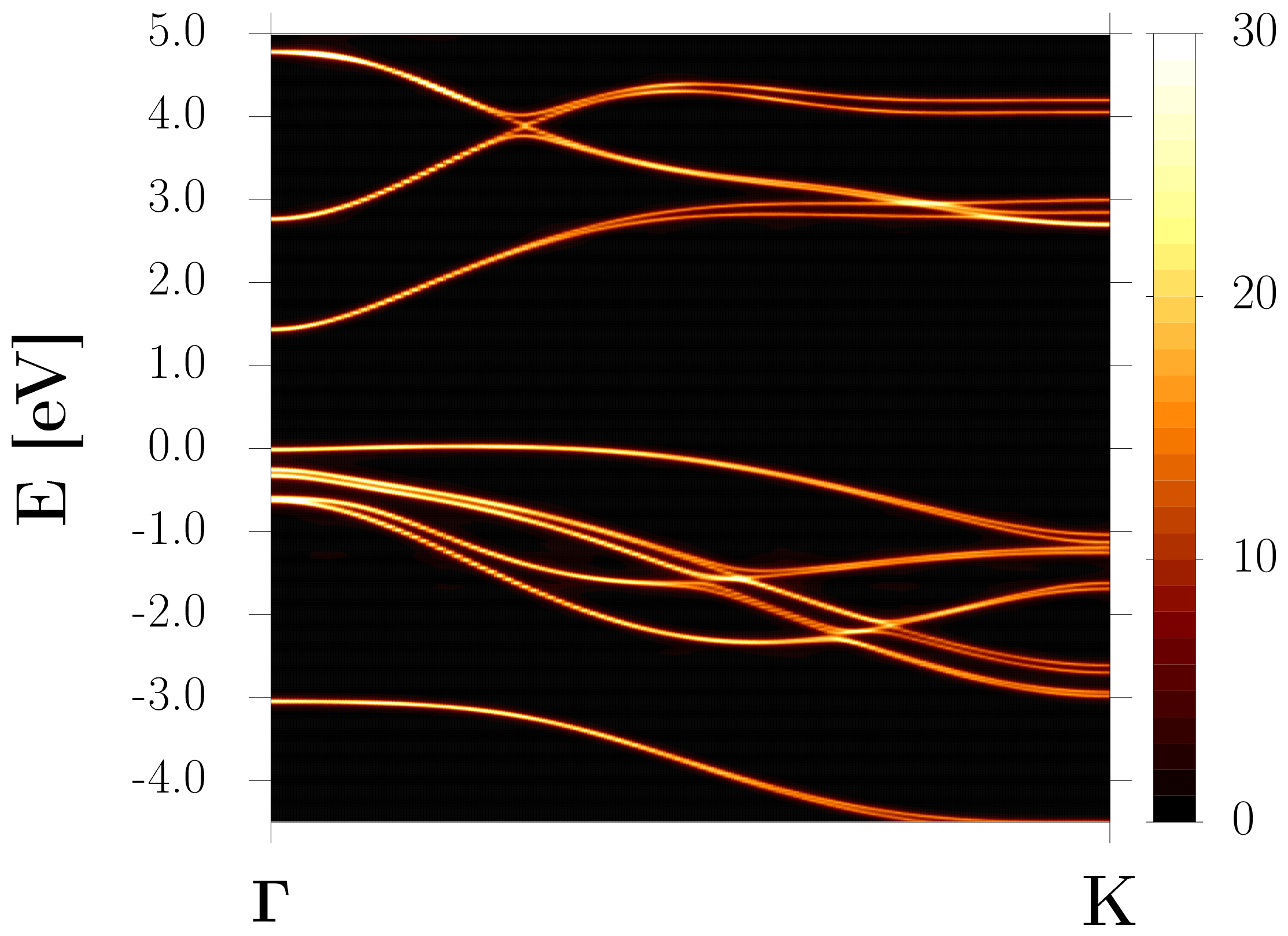
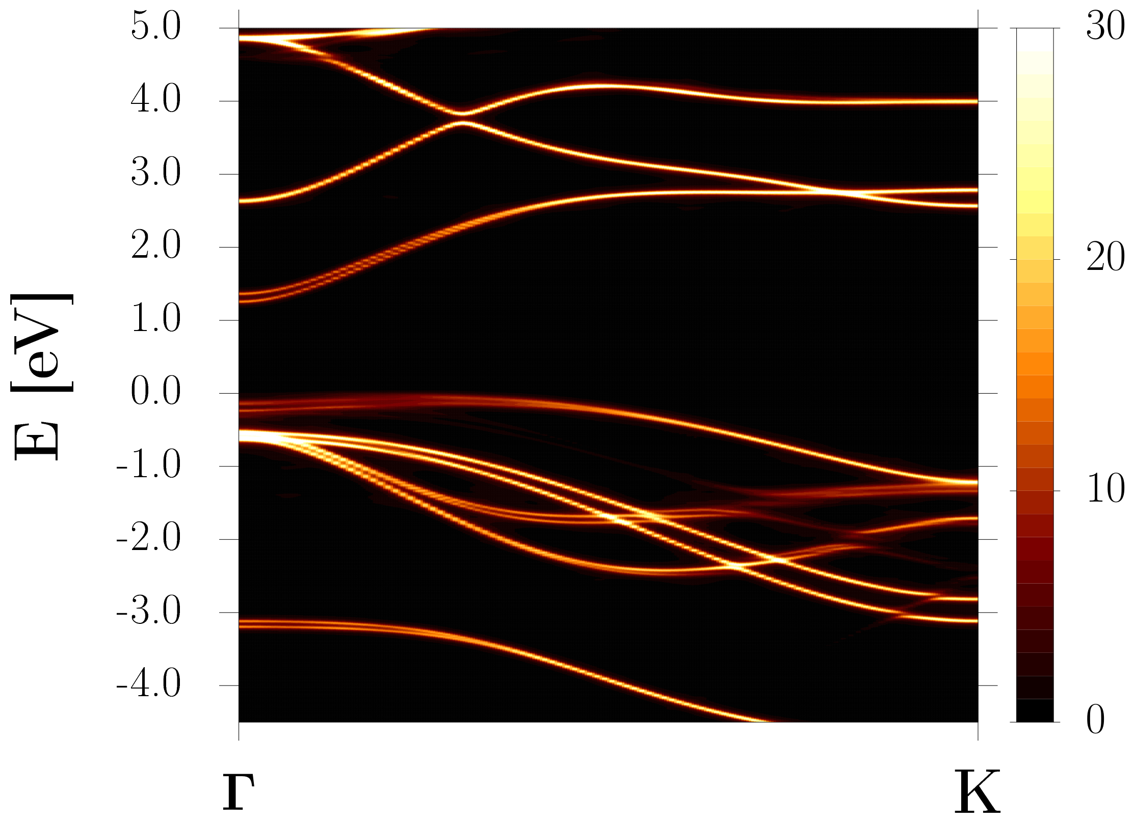
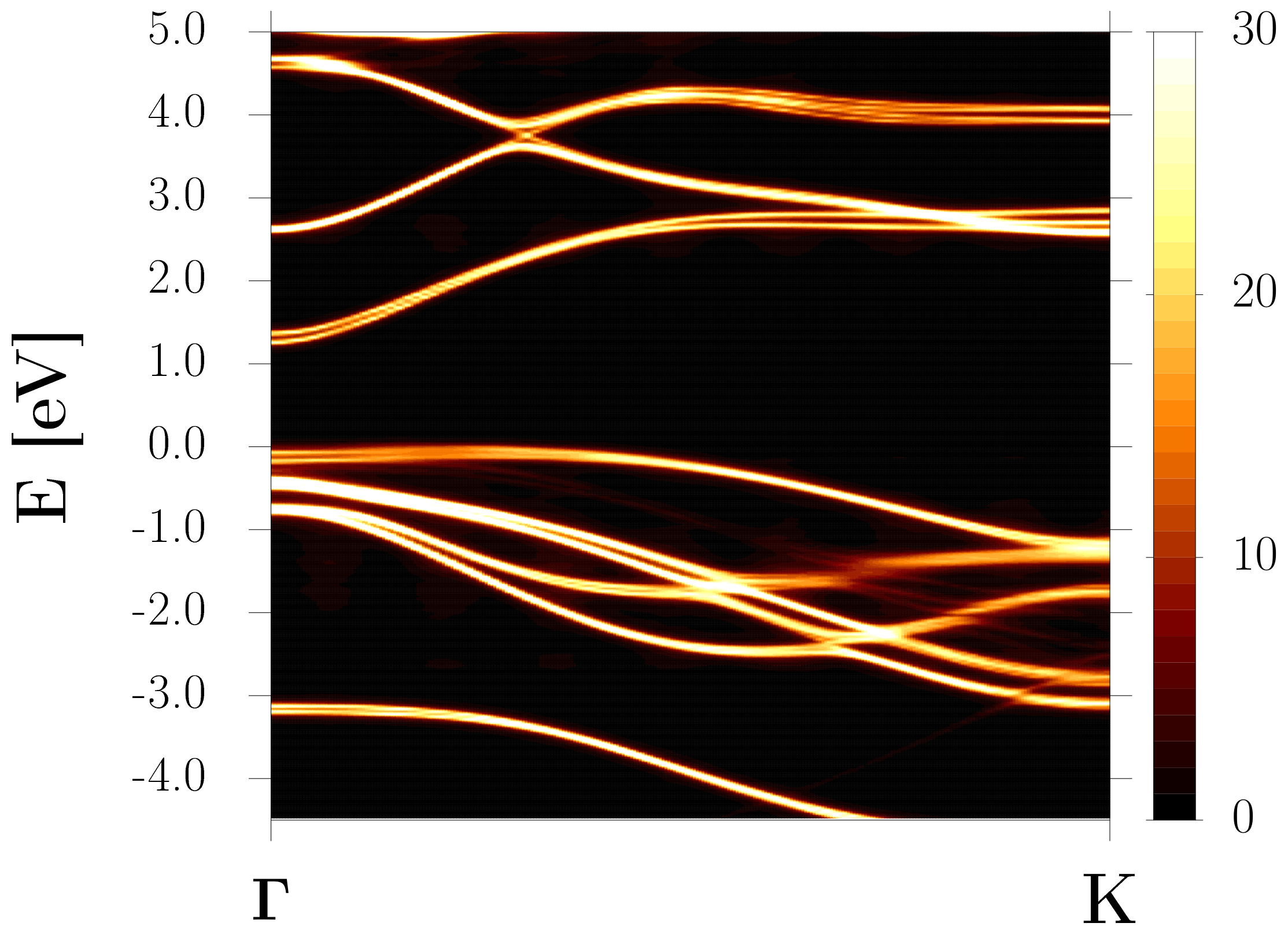
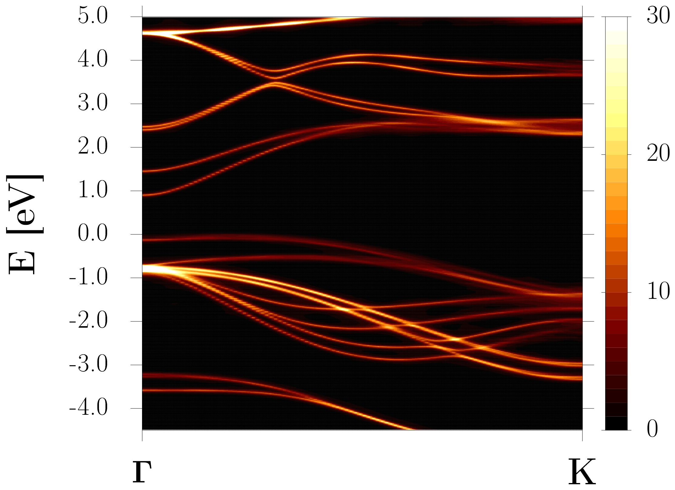
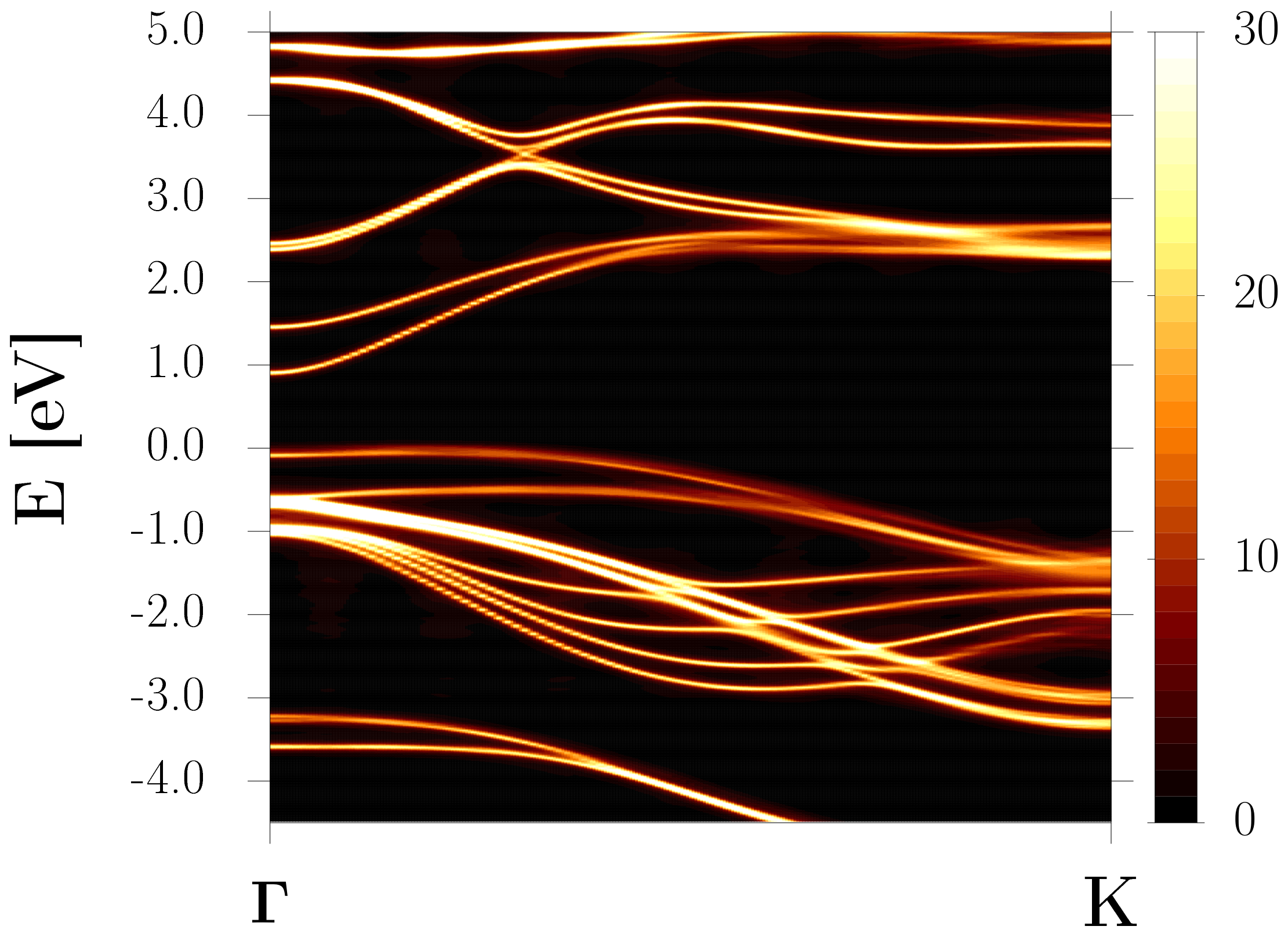
Fig. 2(a) and (b) show the A-type and B-type twisted InSe bilayers, respectively. Motifs corresponding to the different stacking configurations seen in fig. 1 can easily be identified in certain regions of the twisted system. For example, A-1 is seen at the corners of fig. 2(a), whereas the A-2 is seen between the corners and the central region along the direction. Similar atomic structures for twisted InSe bilayers can be seen in a previous study [13]. Fig. 2(c) and (d) also shows the hBN-encapsulated twisted InSe bilayer which will be further discussed below.
A selection of atomic and electronic parameters are displayed for context in table 1, specifically the lattice constant, interlayer distance, binding energy, band gap and effective mass for holes, for the InSe monolayer and for the five InSe bilayers in different stacking configuration. Previous studies [30, 31] on InSe monolayer gave similar calculated results to those obtained here: = 4.05, = 1.45 and = 2.1. The lattice constants and interlayer distances of the InSe bilayer with different stacking configurations are also consistent with previous studies [29, 13]. Note that the optimized lattice constants of InSe bilayers with different stacking configurations are very slightly different, but the difference is below 0.32%. The lattice constant of InSe monolayer (4.059 Å) was therefore adopted for all the calculations of twisted InSe bilayer.
The band gap and binding energy do not deviate significantly from a previous study [29] with the using similar computational methodology. In table 1, the binding energy is seen to be proportional to the interlayer distance, making the B-3 the most stable stacking configuration. It suggests that the repulsion (positive energy) between the atoms is smallest in B-3. This is consistent with the stacking configuration of B-3, because only In atoms in the top and bottom layers are aligned, while the repulsion is strongest between pairs of aligned Se atoms. Yang et al. also proposed that stronger vdW bonding is associated with smaller interlayer distance [29].
In addition, the indirect and direct (calculated from the topmost valence band at ) band gaps decrease as the interlayer distance decreases, consistent with previous studies [29, 32]. The effective masses for holes in the most stable stacking configuration in this work (B-3) are similar to those of a previous study [31]. Along the sequence B-3 A-2 B-1 B-2 A-1 there are clear trends: as the interlayer distance increases, so do the binding energy, band gap and the effective mass for holes. In fact, decreases in hole mass are roughly proportional to decreases in interlayer distance, relative to A-1. The band gap and effective mass for holes are both smaller in all of the InSe bilayers than in the InSe monolayer, as a result of interlayer hybridisation.
| monolayer | A-1 | A-2 | B-1 | B-2 | B-3 | |
| (Å) | 4.059 | 4.058 | 4.067 | 4.059 | 4.058 | 4.071 |
| (Å) | 9.180 | 8.449 | 8.514 | 9.178 | 8.389 | |
| (meV) | -179.52 | -269.74 | -264.23 | -179.84 | -274.22 | |
| (eV) | 1.42 | 1.02 | 0.87 | 0.92 | 1.02 | 0.82 |
| (eV) | 1.50 | 1.08 | 0.94 | 0.99 | 1.08 | 0.90 |
| (m0) | 2.22 | 1.99 | 1.03 | 1.10 | 1.93 | 1.05 |
| (m0) (at ) | -0.83 | -0.96 | -0.70 | -0.74 | -0.94 | -0.66 |
3.2 Relationship between the electronic structure and the stacking configuration of InSe bilayer
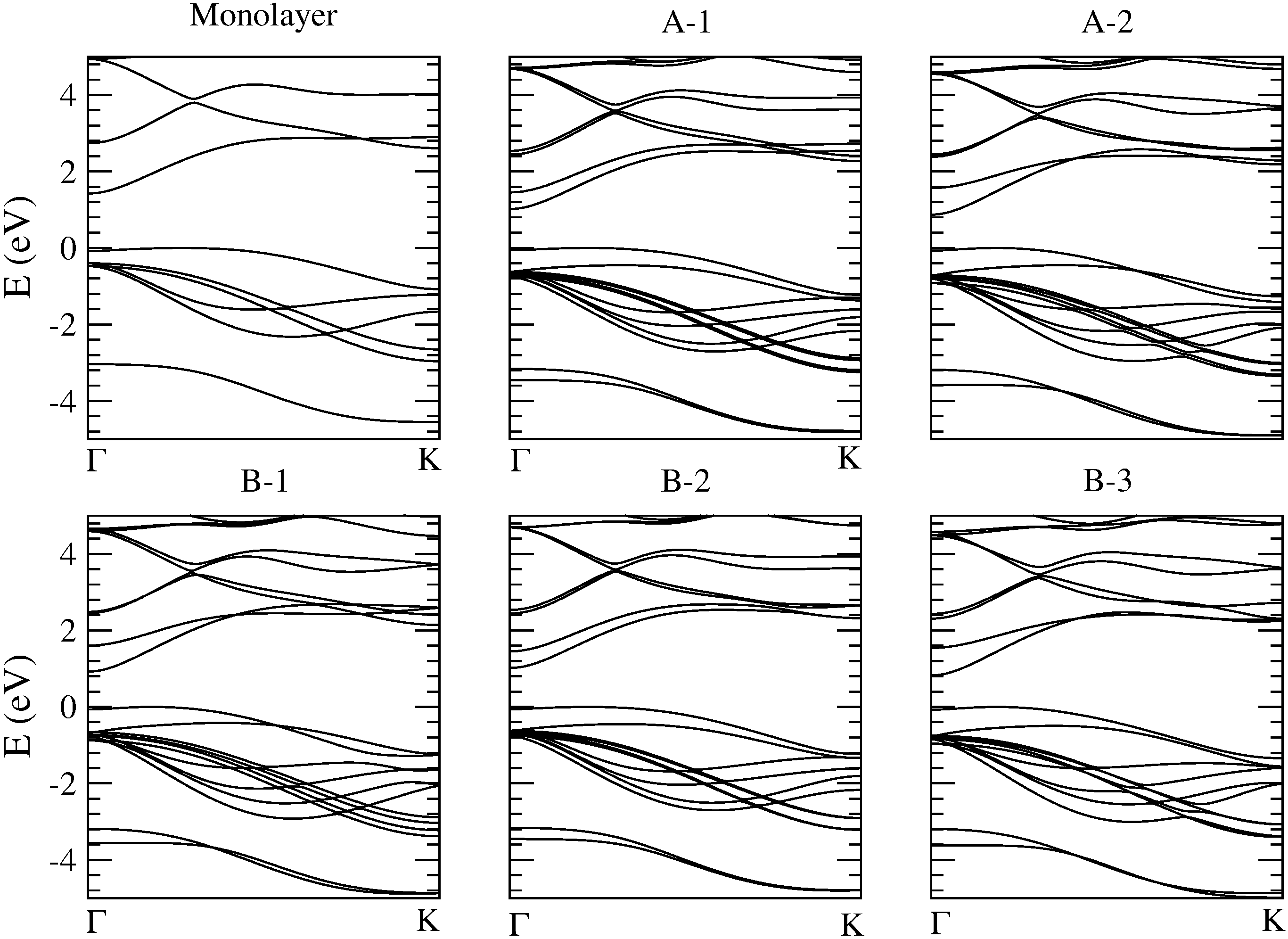
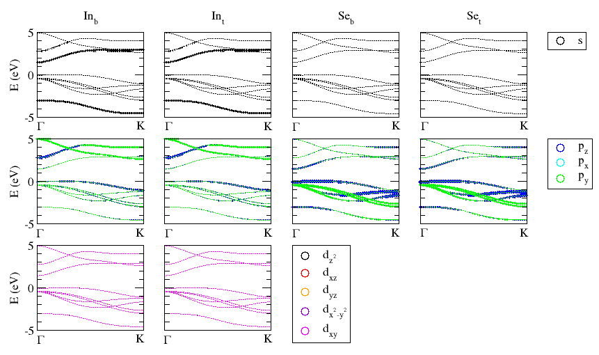
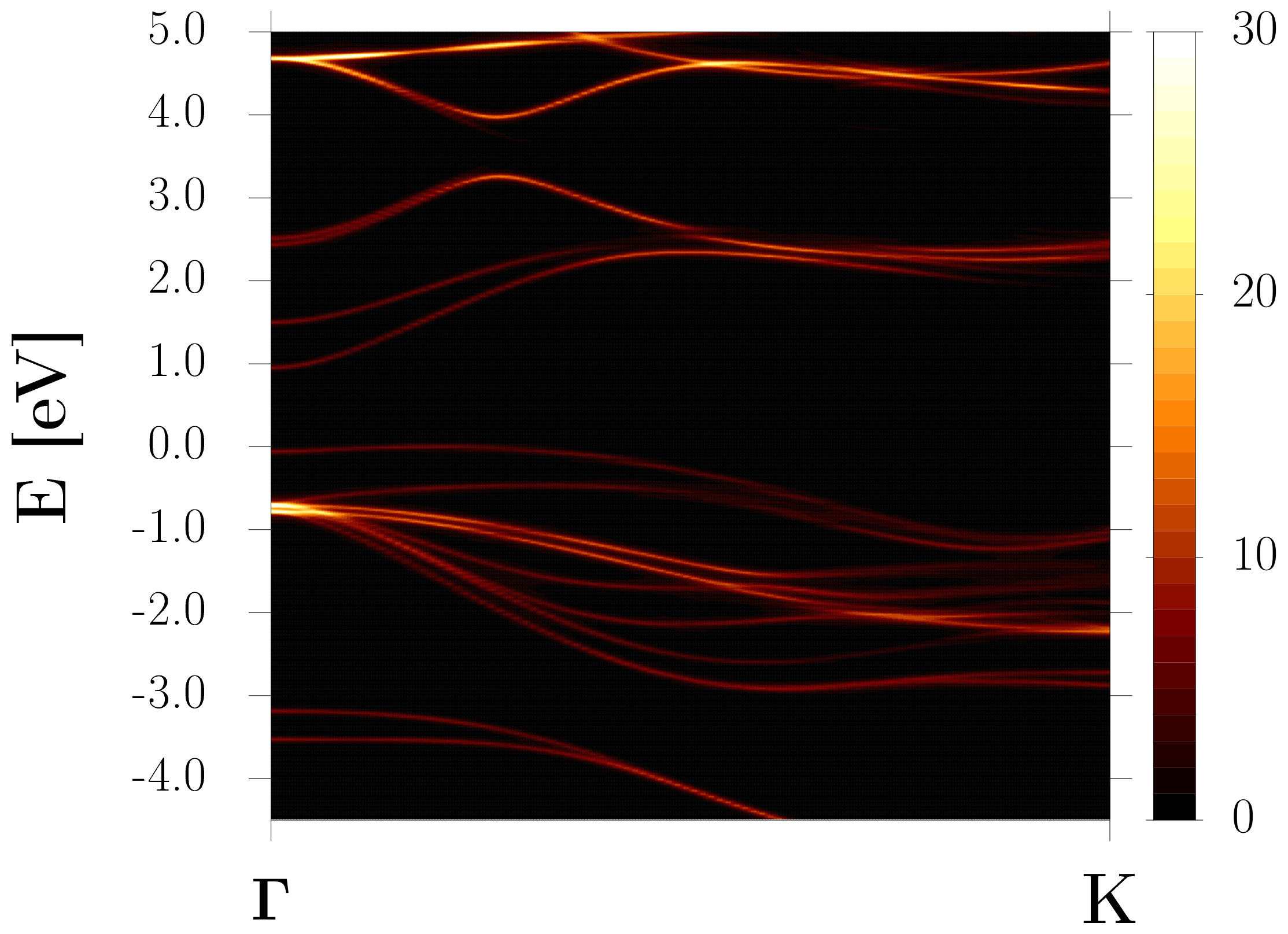
Fig. 3 displays the band structures of InSe monolayer, the A-type and B-type InSe bilayers. We mainly focus on the behaviour of the bands near the VBM in this work. Crucially, band crossings leading to a degeneracy are observed between the topmost two valence bands for stackings A-2 and B-1, whereas these are not seen for A-1 and B-2, while there is a near-crossing for B-3. This is consistent with their stacking configurations: band crossing with a degeneracy happens when there is alignment between In and Se atoms and is not observed for alignment between two Se atoms in the top and bottom layers. It can be seen that it is the topmost VB of the InSe monolayer that hybridises to form these two bands in the InSe bilayer. According to the projected band structure of the InSe monolayer in fig. S1 and table S1, the topmost VB is dominated by the orbitals of Se before 0.74 -K, and by the orbitals of In after. The band repulsion is strongest in A-1 and B-2 and weaker in A-2 and B-1, presumably because the interlayer distance is the smallest for cases with two aligned atoms, leading to there being no band crossing in A-1 and B-2 and band crossing in A-2 and B-1. The ordering of the strength of the band coupling which can be inferred as resulting from pairwise alignment of atoms is therefore Se-Se Se-In In-In. That has the consequence that the splitting of the bands increases as one approaches , due to the increasing orbital contribution of of Se atoms. Similar band structure effects can also seen in a previous study [29] but without discussing the orbital contribution along the kpoint path in detail. It is worth noting that there is no orbital contribution from Se atoms at K for the InSe monolayer.
The band energies of topmost band (labelled VBM) and the band below it (labelled VBM-1) in the InSe bilayer can be modelled, near a crossing, with a simple two-band model and a hybridisation parameter . The eigenvalues of following determinant give the resulting energies after hybridisation [33, 34]:
| (4) |
where two are the energies of the VBMs at k from top and bottom InSe monolayers. describes the interband coupling between two InSe monolayers. The main contributor to is that the orbital contributions vary along a kpoint path.
The projected density of states (PDOS) for the A-type and B-type InSe bilayers (fig. S2) closely resembles that of the InSe monolayer (fig. S1). The details of the orbital contributions of Se atoms are shown in fig. 4. In fig. 4, the classification of orbital contributions of Se atoms is consistent with the previous discussion: A-1 is similar to B-2 and A-2 is similar to B-1, whereas B-3 is distinct. The ordering of Se atom (from black to blue curves) is according to the vertical position (from top to bottom) of Se atom in InSe bilayer. The red and black curves are not seen in the A-1, B-2 and B-3 because they have same magnitudes as the green and blue curves, respectively. This means that the orbitals of the two outermost Se atoms (Sett (black) and Sebb (blue)) are the same. This is also true for the two innermost Se atoms (Sebt (red) and Setb (green)). In general, the orbitals of the outermost Se atoms are only larger than the innermost Se atoms near , excepting the discontinuous behaviour around the intermediate kpoint path and K for the A-2 and B-1.
The discontinuous behaviour that occurs just beyond the midpoint of the kpoint path is the result of to the interband coupling between the VBM and the VBM-1: where a peak occurs for the VBM, there is a trough for the VBM-1 (not shown). The discontinous behaviour in A-2 and B-1 is the same but in reverse, for example, there are peaks for Setb (green) and Sebb (blue) around the kpoint of band crossing in A-2, whereas these two curves display troughs for B-1. The discontinuous behaviour is also reversed for the VBM and VBM-1 in the A-2 or B-1 stackings. Furthermore, the divergence in the PDOS weights on approach to K for A-1 and B-2 also originates from the interband coupling for the two bands below the VBM. From the analysis of PDOS, the orbital contributions around K for these two bands do not approach zero (with values of 0.4), whereas the orbital contributions for the VBM decrease to zero as approaching toward K in InSe monolayer. The orbital contributions of these two bands (below the VBM) fall to zero and the VBM becomes non-zero for the A-1 and B-2. The interlayer coupling between the VBM and VBM-1 related to two Se atoms (Setb and Sebb) can also be seen in the B-1 stacking.
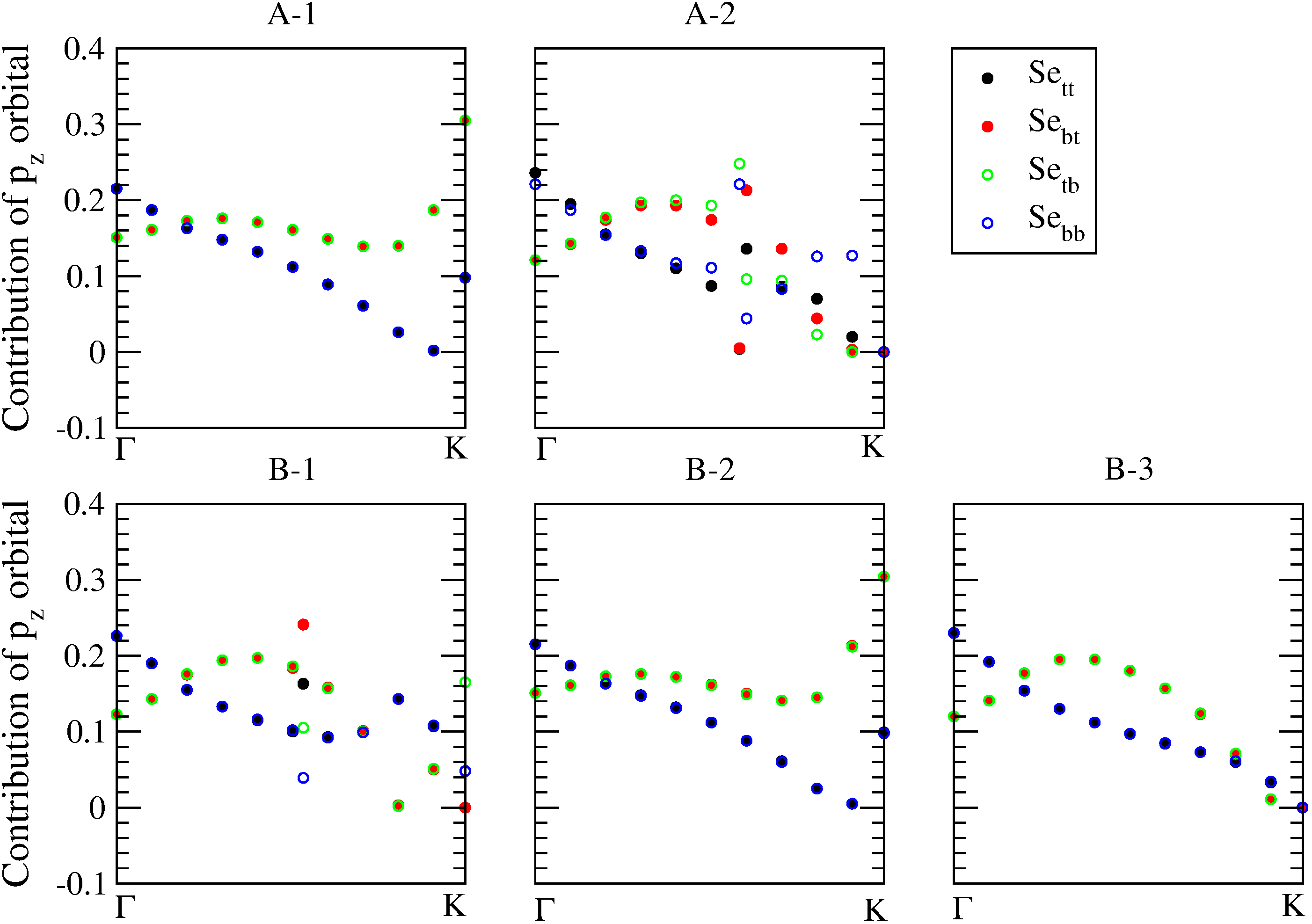
The orbital contributions of the outermost Se atoms (black and blue curves) have the same behaviour as InSe monolayer (if ignoring the sudden increase near K) because they decrease from to K. The orbital contributions of the innermost Se atoms (red and green curves) first increase to 0.3-0.4 -K, then decrease along the kpoint path (if ignoring the sudden increase in the A-1, B-1 and B-2 stackings). The orbital contributions of Se atoms in the B-3 are similar to other stacking configurations but without the weird behaviours mentioned above. There is a more rapid changes for the orbital contributions if the interlayer distance is smaller due to the increase of interlayer coupling strength. It is worth noting that the CBM of InSe monolayer and InSe bilayer are predominated by the delocalised orbitals of In atoms (see table S2).
4 Residual forces in twisted InSe bilayer
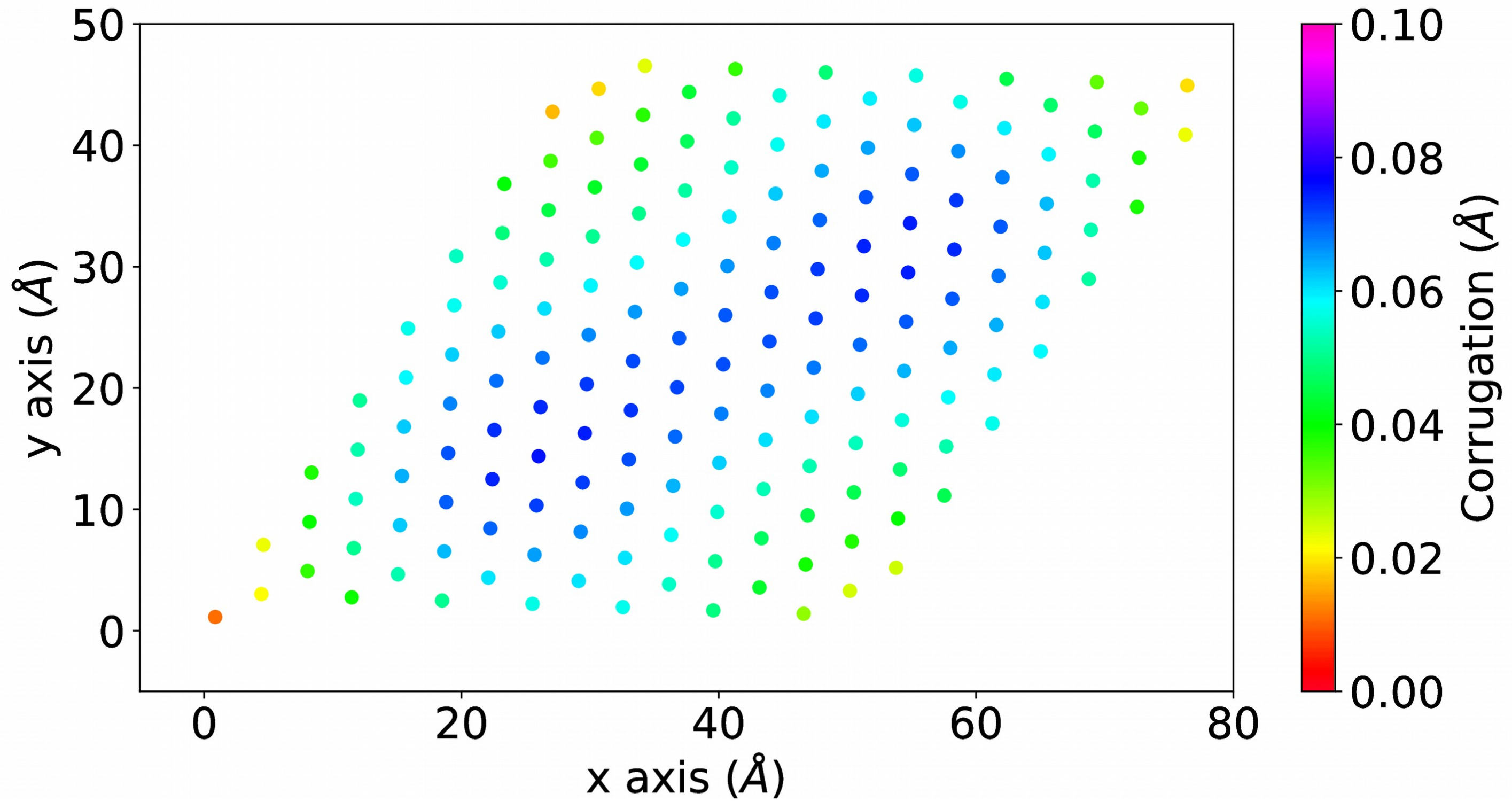
Due to the need for large-scale calculations to study the twisted InSe bilayer at smaller twist angles, we prepare structures with initial corrugations in the z positions, based on the interlayer distances from the structures shown in table 1). A fast Fourier transform (FFT) is used to Fourier interpolate from a small grid corresponding to the known stackings in the corner and midpoints, up to a grid fine enough to provide heights for each layer at each atom position. The magnitude of the corrugation required to pre-optimise the InSe bilayer to generate the twisted InSe bilayer is relatively small (fig. S4), so the effect of corrugation on the effective band structure is marginal (fig. S5). Two neighbouring bands, such as the VBM and VBM-1, are only separated slightly when considering the corrugation in the atomic structure. Corrugation is thus not expected to result directly in the occurrence of flat bands as in twisted hBN bilayer [33].
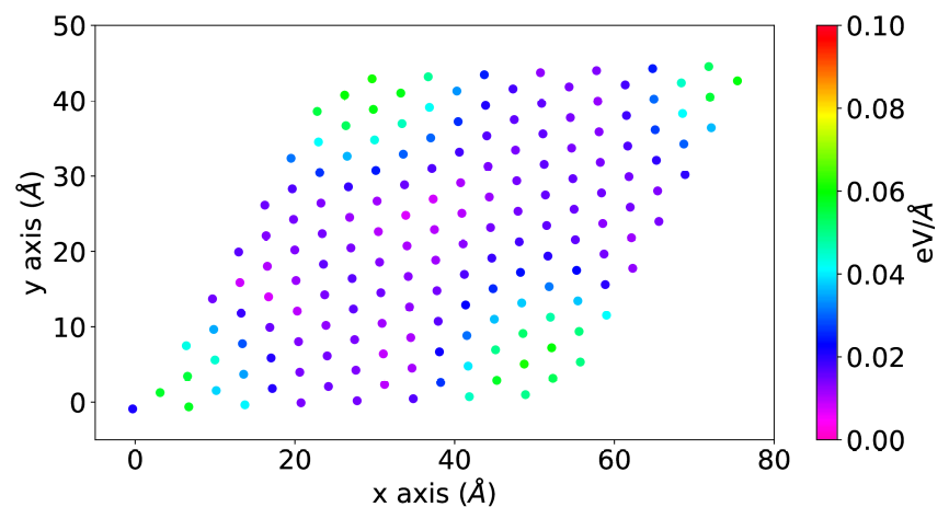
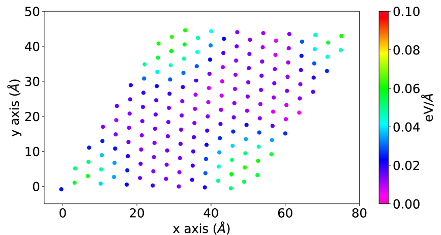
An initial atomic structure is shown in fig. S6 for the A-type twisted InSe bilayer with a twist angle of 4.4o. The corresponding residual total force associated with the innermost atoms (Inbt, Sebt, Intb and Setb) after the calculation of geometry optimisation is displayed in fig. 5. The distribution of residual total force in fig. 5 look similar to fig. S6. The outermost atoms (Intt, Sett, Inbb and Sebb) do not exhibit similar distributions in fig. S6 and their forces are smaller than the innermost atoms (not shown). This phenomenon is suggested to be intrinsic for any twisted bilayer system. The direction of the residual force provide the information of how the atoms move in full structural relaxation until no residual force is retained.
The residual total forces are mainly from the forces along the z direction (compare fig. S8 and fig. S9), implying the larger rearrangement of vertical positions of innermost atoms compared to their in-plane positions (for at least the twist angle considered here). The similarity of the residual force distributions along the x, y and z directions are seen between the neigbouring innermost In and Se atoms, whereas the forces are larger in Se atoms because the distance between two innermost Se atoms is smaller than other combinations of atoms. In addition, the two InSe layers have opposite residual forces along all directions (see fig. S8 for the residual forces in z direction).
4.1 Electronic structure of twisted InSe bilayer
The electronic parameters such as the band gap and the effective mass for holes calculated from the band structure of twisted InSe monolayer (has a twist angle relative to the referenced untwisted InSe monolayer) along the -K of the untwisted InSe monolayer do not change significantly (fig. S3). The main factor that affects the band structure is the interlayer distance, or we can say the stacking configuration, because the interlayer distance is the particular result of the interaction between atoms in a stacking configuration. Shang et al. [32] also showed that the band structure changes with the interlayer distance. The resulting interlayer distance of the twisted InSe bilayer is determined by the proportions of different stacking configurations in the different regions of twisted InSe bilayer. According to table 1, the interlayer distances are within [8.449, 9.180] and [8.389, 9.178] for the A-type and the B-type twisted InSe bilayers, respectively.
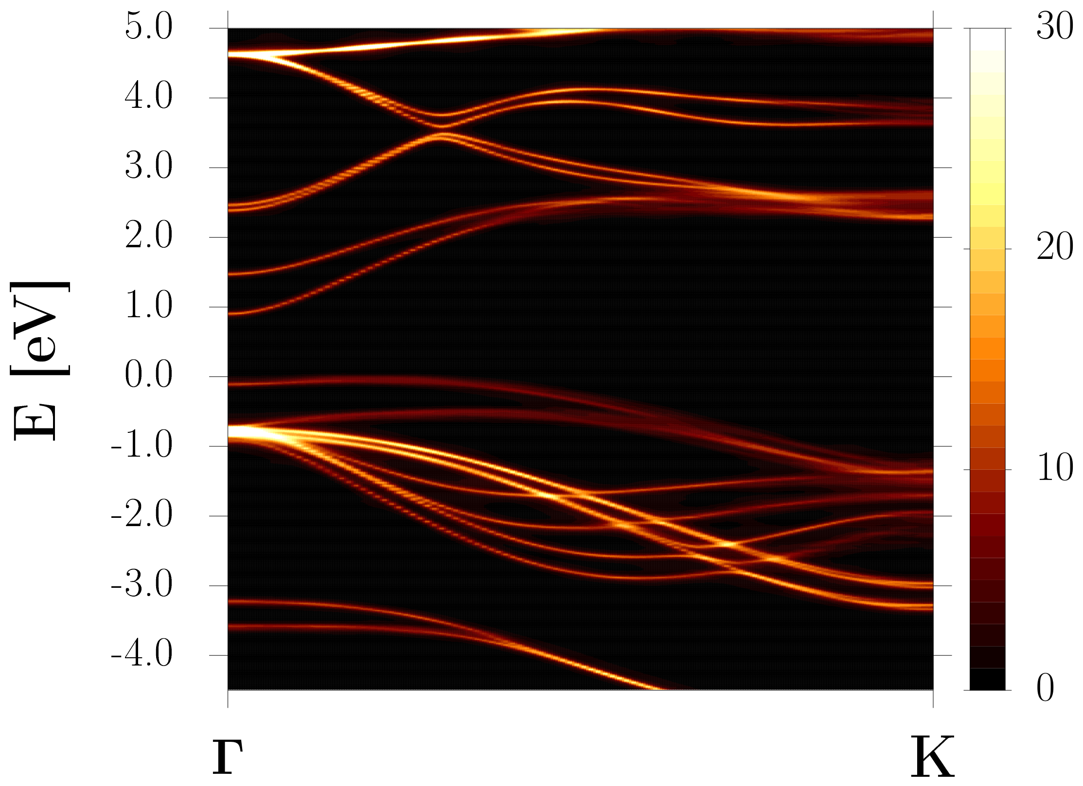
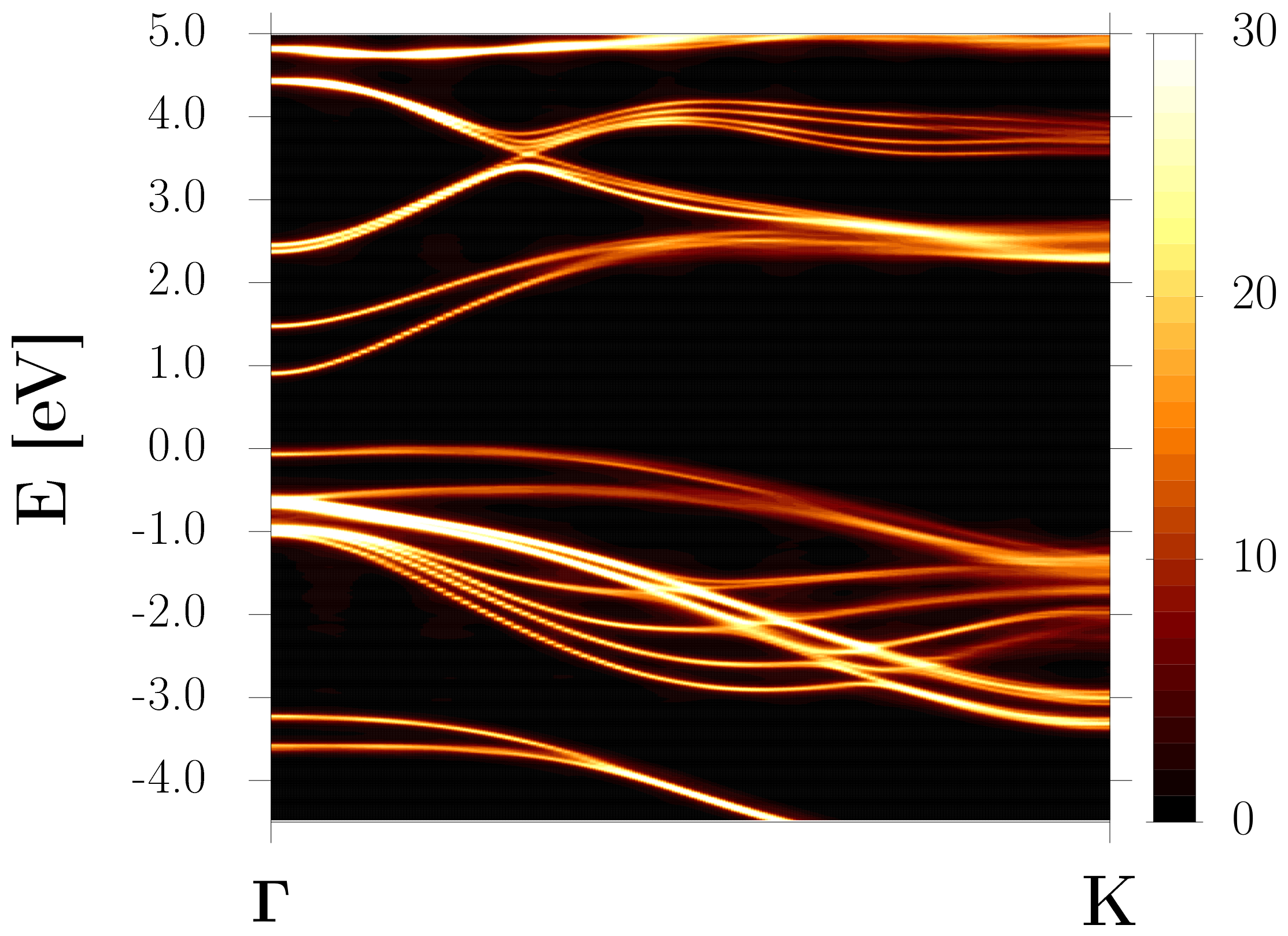
The inclusion of spin-orbit coupling (SOC) in the calculation of the effective band structure leads to the splittings of bands. The splittings of the VBM and CBM are only pronounced near K and around 0.5 -K to K, respectively, for InSe monolayer, twisted InSe bilayers and the hBN-encapsulated twisted InSe bilayers (see fig. S10 and fig. S11). Thus, its effect on the band gap and effective mass for holes can be ignored. It is interesting to see that the avoided crossing of bands around 4 eV is eliminated by the SOC for all systems. The computation effort can be reduced by not considering the SOC in the calculations. In addition, the projection of the effective band structure on the top and bottom layers have larger difference at larger twist angle, whereas the difference is very small at small twist angle (see fig. S3, fig. S14 and fig. S15).
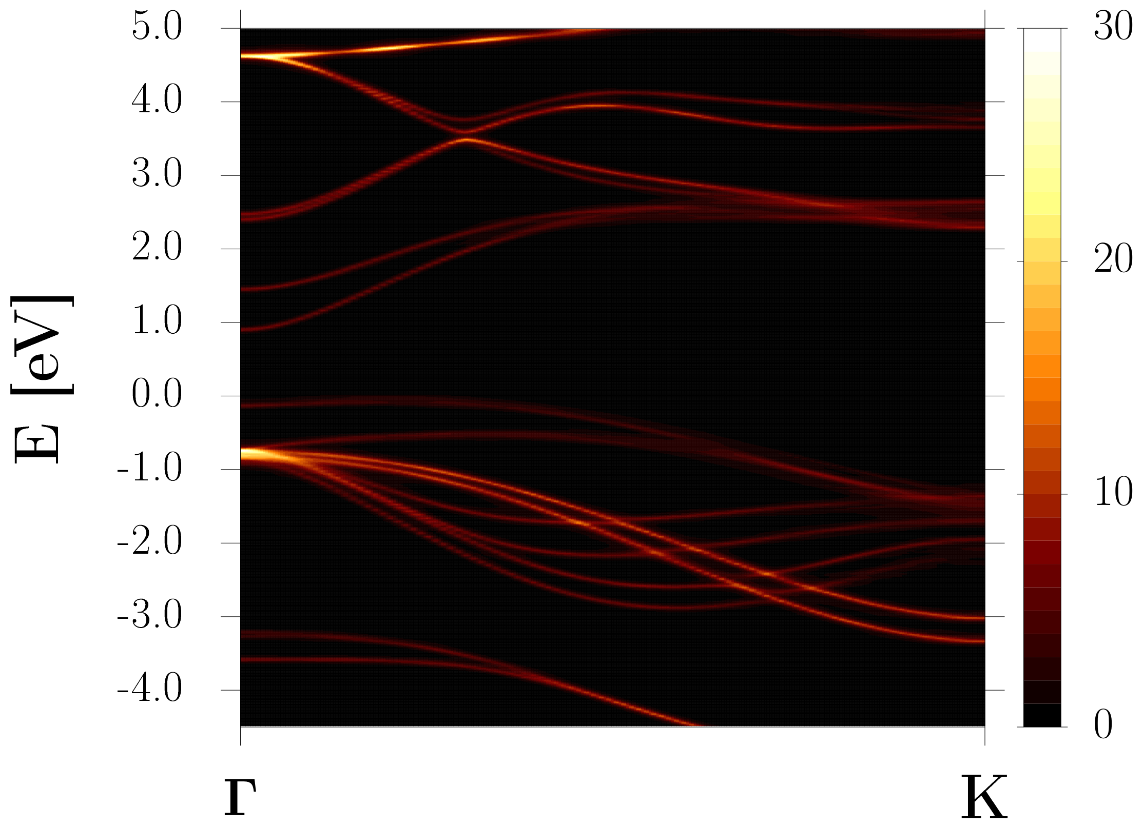
The encapsulation of the hBN layer aims to change the electronic properties of twisted InSe bilayer. The inclusion of twist angle between InSe and hBN layers does not change the band structure [35]. The insertion of the hBN layer only decreases the separation between neigbouring bands such as the VBM and VBM-1 in the twisted InSe bilayers, by increasing the distance between two InSe layers (reducing the interaction between two InSe layers). Similar result can be seen in the hBN-encapsulated black phosphorus [36]. It is worth noting that the anti-crossing bands appear near K within the range of [-2.0, -1.0] eV. The effective band structure of the hBN-encapsulated twisted InSe bilayer is suggested to approach the band structure of InSe monolayer. This is because the projection of the hBN-encapsulated twisted InSe bilayer onto the hBN layer and its PDOS both show that the VBM of the hBN layer is at least 1.5 eV below the Fermi level, thus the VBM of twisted InSe bilayer is not affected by the hBN (fig. S12 and fig. S13).
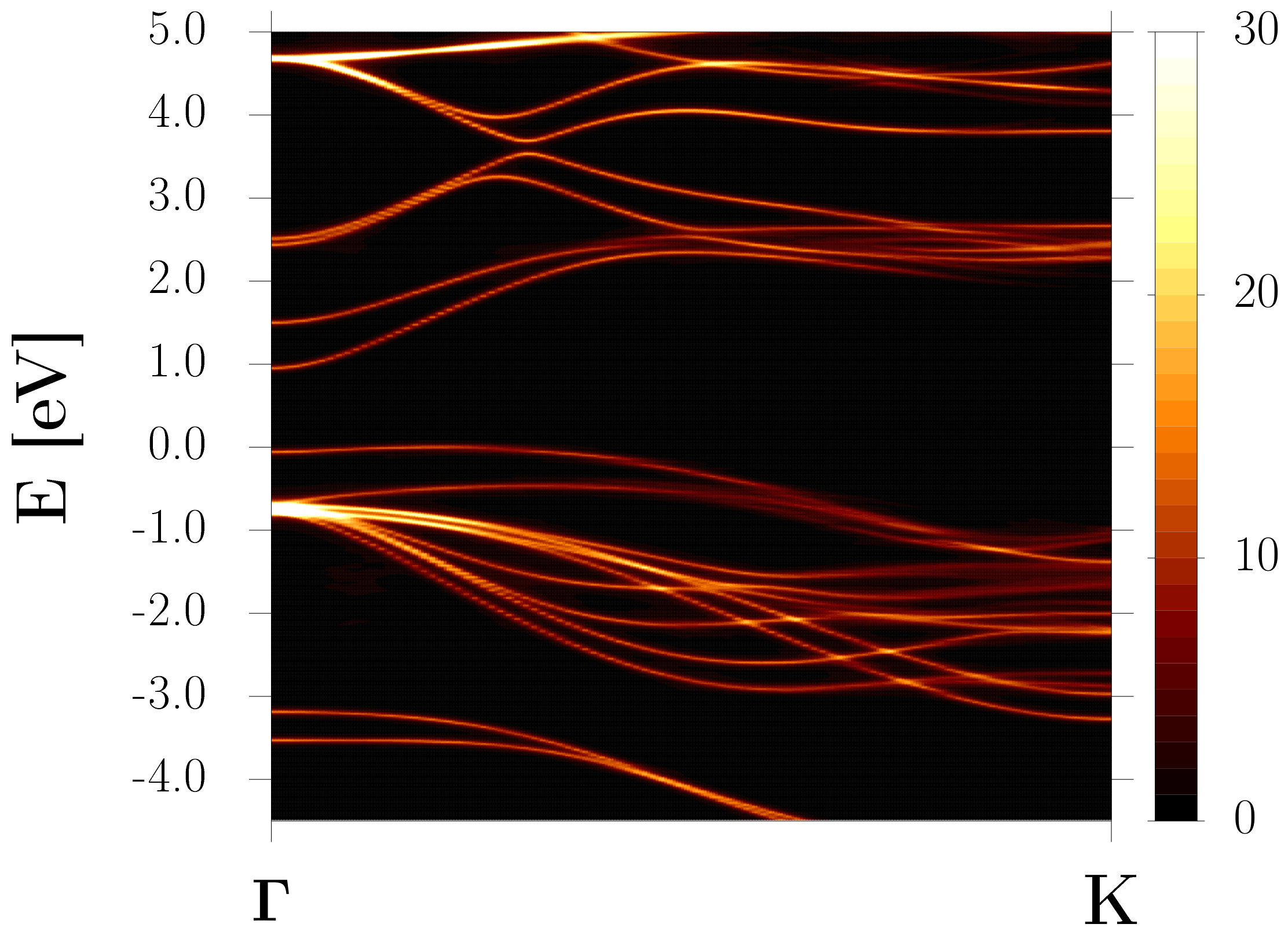
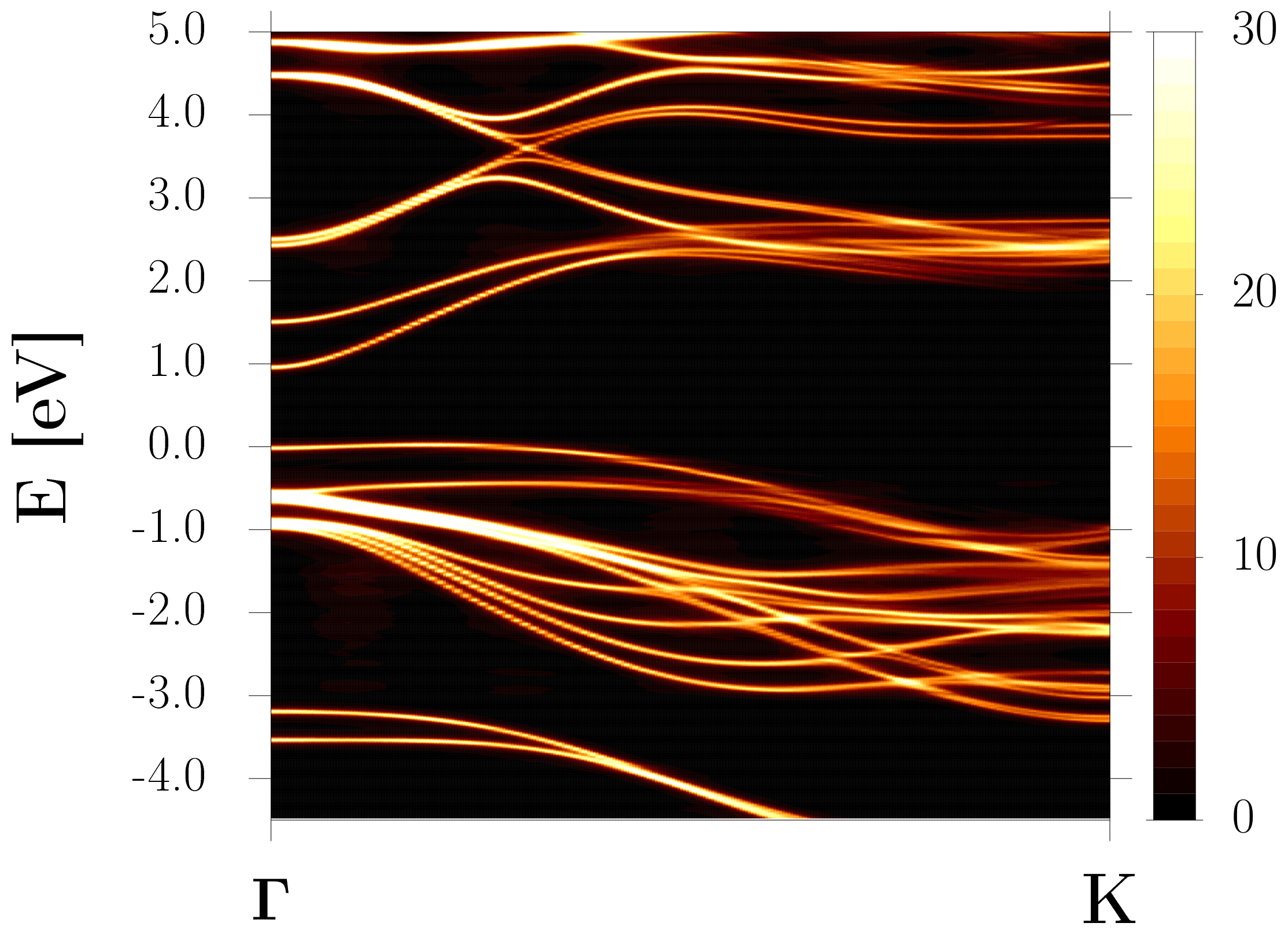
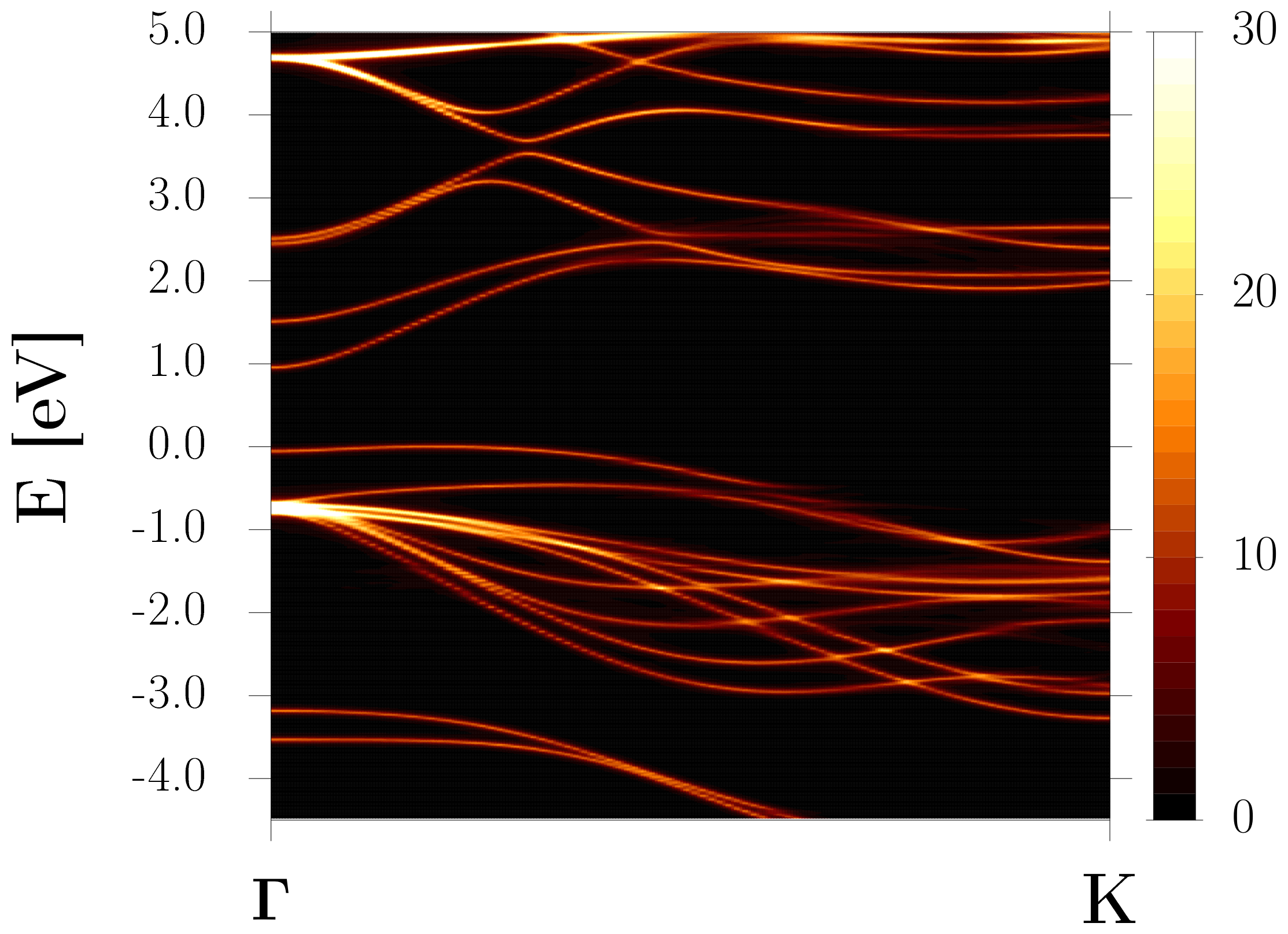
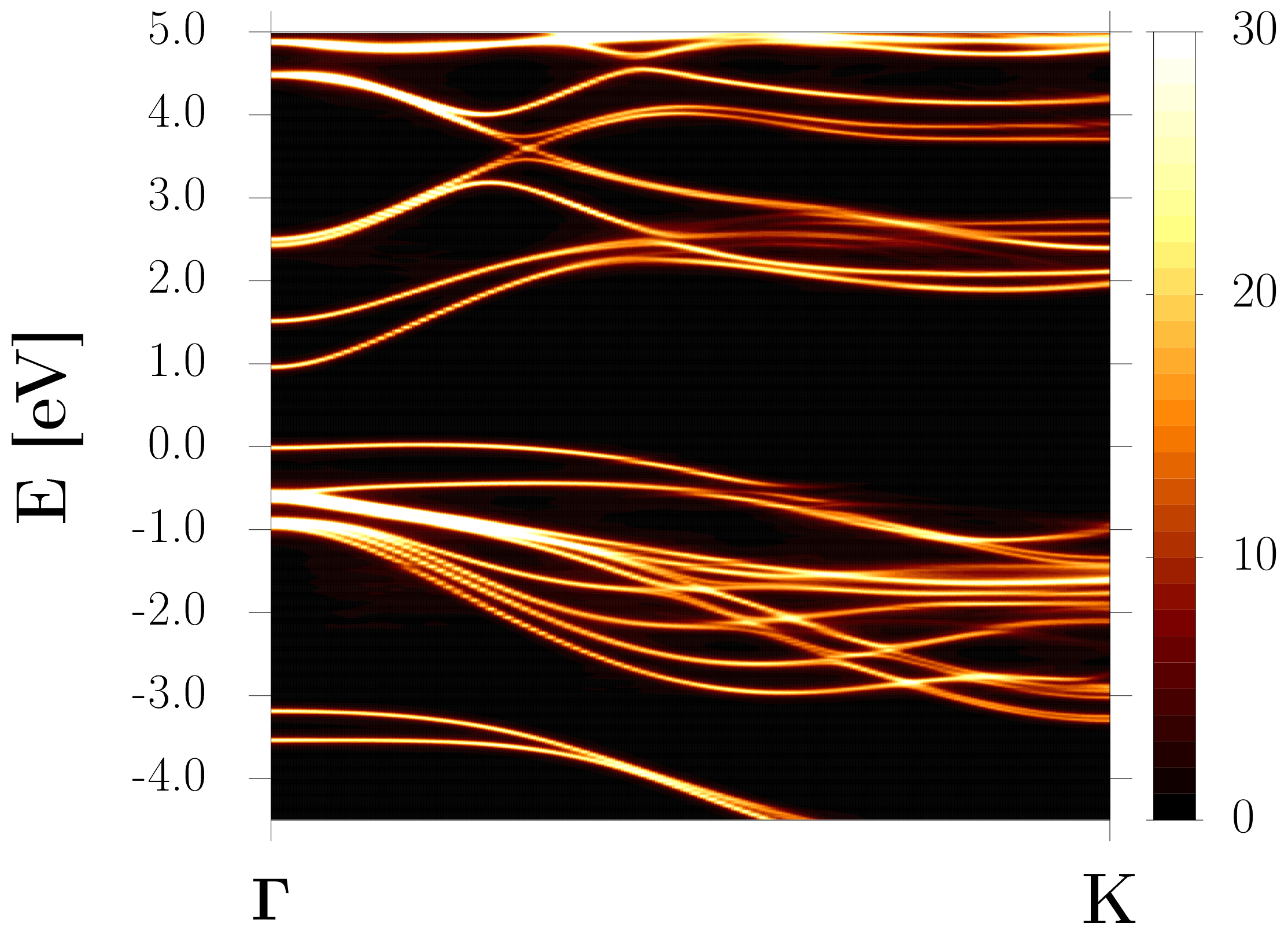
We are interested to know the effect of the different stacking configurations seen on the atomic structure of the twisted system on its band strcuture (fig. 2(a) and (b)). In fig. 6, the VBM of twisted InSe bilayer can be well-described by the same band of aligned InSe bilayer from the primitive cell calculation with the same interlayer distance. In fig. 6(a), the green and blue curves represent the bands in the A-1 and A-2 stackings, from the primitive cell calculations. The isosurfaces of charge densities in fig. 6(b) and (c) show the charge density localised around the regions corresponding to the A-1 and A-2, respectively. The finite-width bands in the effective band structure was calculated by using the spectral function unfolding method. They are contributed by the A-1, A-2 and their combinations when analysing through the isosurfaces of the charge densities. The argument also applies to the twisted InSe bilayer with considering SOC in the calculation (fig. S16). The result is partly different from twisted hBN bilayer [33] (its stacking configurations is similar to InSe bilayer) because the VBM is contributed by the A-1 stacking. However, the VBM is contributed by the A-2 stacking in twisted InSe bilayer at smaller twist angles in the previous study [13]. It is suggested that the charge densities for the VBM in our calculations may further localised in the A-2 if the twist angle is smaller than 3o. The flat bands is suggested to appear at small twist angles (magic angles are unnecessary) for twisted bilayer system composed of polar 2D semiconductor [33]. Zhao et.al. proposed that the flat bands can be obtained by reducing the sublattice symmetry of twisted system, which means increasing the difference of the atoms in the unit cell [33].
The length from to the lowest energy kpoint of the VBM equals to the length of kpoint path of the top InSe layer inside the first Brillouin zone of the bottom InSe layer: these are 0.886 -K and 0.867 -K for a twist angle of 17.9o and 27.8o, respectively (see fig. S17(c)-(f)). This phenomenon can also be seen in fig. S3 for the band structures of various twist angles considered in InSe monolayer. Furthermore, we have noticed that there is approximately no difference between the effective band structures of the A-type and B-type twisted systems at the same twist angle in fig. S17 because of the similarity of the band structure between A-type and B-type InSe bilayers in fig. 3. This is similar to the results in previous literature [37].
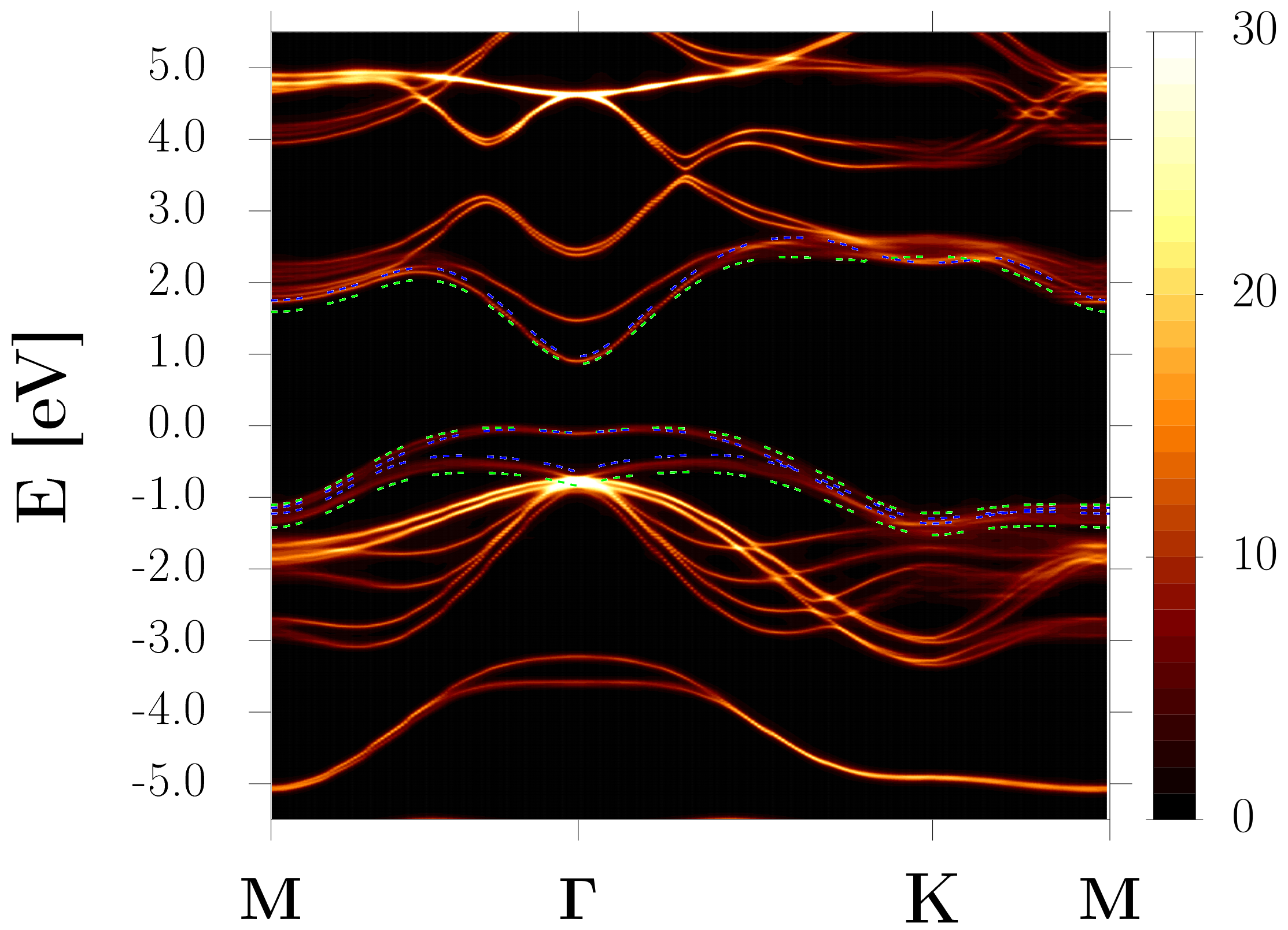
It is worth noting that the effect due to the difference of the lattice constant for different stacking configurations seen in some regions of twisted InSe bilayer can be ignored (fig. S18). The flatness of the VBM around the highest energy kpoint increases (so the effective mass for holes increases) if the interlayer distance increases (fig. S19), consistent with table 1. However, the interlayer distances of the A-type and B-type twisted InSe bilayers with various twist angles considered in this work are 8.850.04 Å (fig. S20), similar to the small variation of interlayer distance for twist angles between 13.2o and 32.2o in previous studies [37]. The small variation of interlayer distance at different twist angles implies that the proportion of each stacking configuration in the same type of twisted InSe bilayer only change slightly.
The curvatures of the VBMs which determine the effective mass for holes with different twist angles considered in this work seem kept at a constant (fig. S21). Different band foldings at different twist angles lead to the variation of flatness of the VBM, as seen in the previous literature [13]. The defect states are proposed to be formed in polar 2D semiconductor at sufficiently small twist angles and this leads to the appearance of flat bands due to the weak interactions with other host and defect states [33]. Furthermore, the studies of twisted MoS2 bilayer showed that the inhomogeneous interlayer hybridisation and the local strain can also lead to the flat bands [38]. We may possibly see the flat bands in twisted InSe bilayer if further decreasing the twist angles to smaller than 3o, as seen in the previous study [13]. The variation of band gap is small, it is 0.950.03 eV for all twist angles in both the A-type and B-type twisted systems considered in this work. This small variation of band gap does not deviate from the results of previous studies [37].
5 Calculated exciton binding energy in twisted InSe bilayer and twisted InSe/hBN/InSe heterostructure
According to the work of Viner et al. [39] (detailed calculations are shown in supporting information), we can estimate the intralayer and interlayer exciton binding energies of twisted InSe bilayer based on the effective mass for holes obtained here. In the previous literature [40], the band dispersion of GGA-PBE and GW were in good agreement except for the GW have larger band gap than the GGA-PBE. The calculated exciton binding energies in the environments of vacuum and hBN are shown in table 2, table 3 and figure 7.
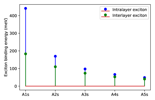
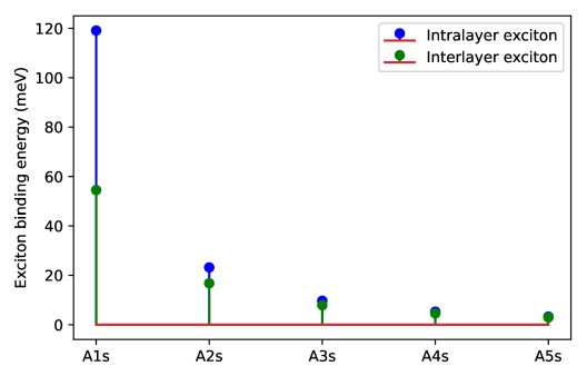
The A1s intralayer exciton binding energies in both environments are more than 2X larger than the A1s interlayer exciton binding energies. From A2s to A5s, their difference gradually decreases to 8 meV and 0 meV, in the enviroments of vacuum and hBN, respectively. Furthermore, the intralayer and interlayer exciton binding energies in the environment of vacuum are 3.7X and 3.4X larger than in the enviroment of hBN.
In addition, the similarity between the hBN-encapsulated twisted InSe bilayer and InSe monolayer can be seen through the same analysis as fig. 6(a). The VBM of InSe monolayer from the primitive cell calculation match well with the effective band structure of the hBN-encapsulated A-type and B-type twisted InSe bilayers from the supercell calculations (fig. S22). The calculated intralayer exciton binding energies in the environment of vacuum and hBN are shown in table 4. In the calculation, (eq. (13) in the supporting information) was used as the Coulomb potential because the trilayer heterostructure system can be regarded as two separated InSe layers plus a hBN layer. The result in the environment of vacuum is 1.7X larger than in the environemnt of hBN for A1s intralayer exciton binding energy.
| A1s | A2s | A3s | A4s | A5s | |
|---|---|---|---|---|---|
| Intralayer exciton (meV) | 441.1 | 169.6 | 97.5 | 66.1 | 48.7 |
| Interlayer exciton (meV) | 183.2 | 110.1 | 73.4 | 52.8 | 40.4 |
| A1s | A2s | A3s | A4s | A5s | |
|---|---|---|---|---|---|
| Intralayer exciton (meV) | 119.1 | 23.2 | 9.7 | 5.3 | 3.3 |
| Interlayer exciton (meV) | 54.5 | 16.8 | 7.9 | 4.6 | 3.0 |
| A1s | A2s | A3s | A4s | A5s | |
|---|---|---|---|---|---|
| Intralayer exciton (meV) (vacuum) | 232.9 | 60.9 | 27.4 | 15.5 | 9.9 |
| Intralayer exciton (meV) (hBN) | 138.8 | 27.8 | 11.5 | 6.2 | 3.9 |
6 Conclusions
The atomic and electronic parameters of InSe monolayer and InSe bilayers with different stacking configurations are discussed in this work. The binding energy, band gap and effective mass for holes increase as the interlayer distance increases. The most stable stacking configuration is the B-3. The stacking configuration with the largest band gap and the effective mass for holes are the A-1. The band gap and the effective mass for holes in InSe monolayer are larger than InSe bilayer with different stacking configurations because there is no interlayer hybridisation in the monolayer form.
Only the band structure of the A-2 and B-1 show the band crossings for the two bands below the Fermi level. The orbitals of Se atoms and orbitals of In atoms give the largest contributions to the VBM and CBM, respectively, for InSe monolayer and InSe bilayer with different stacking configurations. The variation of the VBM in InSe bilayer with different stacking configurations can be explained by the variation of the orbital contribution of each Se atom.
The residual force in each innermost atom displays a similar distribution with the distribution of interlayer distance according to the regions corresponding to each stacking configuration in twisted InSe bilayer. The residual forces in the outermost atoms are smaller than the innermost atoms because there is a direct interaction between the innermost atoms in the two different layers. The same reason also leads to the larger residual forces for innermost Se atoms than In atoms. The innermost atoms mostly do the vertical movements when forming twisted system (for at least the twist angle considered here) from the analysis of residual force.
The spin-orbit coupling does not change significantly the VBM, especially around the highest energy kpoint of the VBM where we concern. The variation of the VBM near K and around the kpoint we concern becomes larger and remains the same as the twist angle increases, respecstively. The effective band structure of the A-type (B-type) twisted InSe bilayer with acceptable lattice mismatch can be well described by the A-type (B-type) InSe bilayer with different stacking configurations from the primitive cell calculations. It is necessary to include the bands from both the top and bottom InSe layers from the primitive cell calculations along the same kpoint path (especially at large twist angles) for getting a better mapping on the twisted InSe bilayer.
The effective mass for holes will increase if the interlayer distance in twisted InSe bilayer increases. However, the interlayer distance of A-type and B-type twisted InSe bilayers with different twist angles considered in this work are 8.850.04 Å. The differences of effective mass of holes and band gap among different twist angles are very small, they are calculated to be 1.570.18 mo and 0.950.03 eV, respectively.
The curvature of the VBM becomes less obvious owing to the increase of band folding as the twist angle decreases and not owing to the changes of the VBM at different twist angles. The effective mass for holes of InSe bilayer at different twist angles are approximately the same and the exciton binding energies were calculated to be 441.1 meV and 119.1 meV for A1s intralayer excitons in the environments of vacuum and hBN, respectively. While the A1s interlayer exciton binding energies are 183.2 meV and 54.5 meV in the environments of vacuum and hBN, respectively.
In addition, the hBN layer in the twisted InSe/hBN/InSe heterostructuere only decreases the interlayer hybridisation between two InSe layers. A good match between the effective band structure of twisted InSe/hBN/InSe heterostructure and the bands of InSe monolayer from the primitive cell calculation can also be seen. This gives A1s intralayer exciton binding energies of 232.9 meV and 138.8 meV in the environments of vacuum and hBN, respectively.
7 Acknowledments
The Engineering and Physical Sciences Research Council supported N.D.M.H through grant EP/P01139X/1. S.M.L were supported by University of Warwick Chancellor’s Scholarships. Computing resources were provided by the Scientific Computing Research Technology Platform of the University of Warwick, and the UK national high performance computing service, ARCHER and ARCHER2, via the UKCP consortium (EP/P022561/1). We acknowledge the use of Athena at HPC Midlands+, which was funded by the EPSRC through Grant No. EP/P020232/1.
References
- [1] H. C. Po, L. Zou, A. Vishwanath, and T. Senthil. Origin of mott insulating behavior and superconductivity in twisted bilayer graphene. Phys. Rev. X, 8:031089, 2018. https://doi.org/10.1103/PhysRevX.8.031089.
- [2] G. Tarnopolsky, A. J. Kruchkov, and A. Vishwanath. Origin of magic angles in twisted bilayer graphene. Phys. Rev. Lett., 122:106405, 2019. https://doi.org/10.1103/PhysRevLett.122.106405.
- [3] G. T. de Laissardière, D. Mayou, and L. Magaud. Localization of Dirac electrons in rotated graphene bilayers. Nano Lett., 10:804–808, 2010. https://doi.org/10.1021/nl902948m.
- [4] J. M. B. Lopes dos Santos, N. M. R. Peres, and A. H. Castro Neto. Continuum model of the twisted graphene bilayer. Phys. Rev. B, 86:155449, 2012. https://doi.org/10.1103/PhysRevB.86.155449.
- [5] S. Venkateswarlu, A. Honecker, and G. T. de Laissardière. Electronic localization in twisted bilayer MoS2 with small rotation angle. Phys. Rev. B, 102:081103(R), 2020. https://doi.org/10.1103/PhysRevB.102.081103.
- [6] Z. Zhan, Y. Zhang, P. Lv, H. Zhong, G. Yu, F. Guinea, J. Á. Silva-Guillén, and S. Yuan. Tunability of multiple ultraflat bands and effect of spin-orbit coupling in twisted bilayer transition metal dichalcogenides. Phys. Rev. B, 102:241106(R), 2020. https://doi.org/10.1103/PhysRevB.102.241106.
- [7] F. Wu, T. Lovorn, and A. H. MacDonald. Topological exciton bands in moiré heterojunctions. Phys. Rev. Lett., 118:147401, 2017. https://doi.org/10.1103/PhysRevLett.118.147401.
- [8] N. Liu, J. Zhang, S. Zhou, and J. Zhao. Tuning the electronic properties of bilayer black phosphorene with the twist angle. J. Mater. Chem. C, 8:6264–6272, 2020. https://doi.org/10.1039/d0tc00062k.
- [9] C. R. Woods, P. Ares, H. Nevison-Andrews, M. J. Holwill, R. Fabregas, F. Guinea, A. K. Geim, K. S. Novoselov, N. R. Walet, and L. Fumagalli. Charge-polarized interfacial superlattices in marginally twisted hexagonal boron nitride. Nat. Commun., 12:347, 2021. https://doi.org/10.1038/s41467-020-20667-2.
- [10] C. Sun, H. Xiang, B. Xu, Y. Xia, J. Yin, and Z. Liu. Ab initio study of carrier mobility of few-layer InSe. Appl. Phys. Express, 9:035203, 2016. https://doi.org/10.7567/APEX.9.035203.
- [11] D. A. Bandurin, A. V. Tyurnina, G. L. Yu, A. Mishchenko, V. Zólyomi, S. V. Morozov, R. K. Kumar, R. V. Gorbachev, Z. R. Kudrynskyi, S. Pezzini, Z. D. Kovalyuk, U. Zeitler, K. S. Novoselov, A. Patanè, L. Eaves, I. V. Grigorieva, V. I. Fal’ko, A. K. Geim, and Y. Cao. High electron mobility, quantum hall effect and anomalous optical response in atomically thin InSe. Nature Nanotech., 12(223-227), 2017. https://doi.org/10.1038/nnano.2016.242.
- [12] Y. Sun, S. Luo, X.-G. Zhao, K. Biswas, S.-L. Li, and L. Zhang. InSe: a two-dimensional material with strong interlayer coupling. Nanoscale, 10:7991–7998, 2018. https://doi.org/10.1039/C7NR09486H.
- [13] P. Kang. Indirect-to-direct bandgap transition in bilayer InSe: roles of twistronics. 2D Mater., 7:021002, 2020. https://doi.org/10.1088/2053-1583/ab6707.
- [14] P. Giannozzi, S. Baroni, N. Bonini, M. Calandra, R. Car, C. Cavazzoni, D. Ceresoli, G. L. Chiarotti, M. Cococcioni, I. Dabo, A. D. Corso, S. de Gironcoli, S. Fabris, G. Fratesi, R. Gebauer, U. Gerstmann, C. Gougoussis, A. Kokalj, M. Lazzeri, L. Martin-Samos, N. Marzari, F. Mauri, R. Mazzarello, S. Paolini, A. Pasquarello, L. Paulatto, C. Sbraccia, S. Scandolo, G. Sclauzero, A. P. Seitsonen, A. Smogunov, P. Umari, and R. M. Wentzcovitch. QUANTUM ESPRESSO: a modular and open-source software project for quantum simulations of materials. J. Phys.: Condens. Matter, 21:395502, 2009. https://doi.org/10.1088/0953-8984/21/39/395502.
- [15] P. Giannozzi, O. Andreussi, T. Brumme, O. Bunau, M. B. Nardelli, M. Calandra, R. Car, C. Cavazzoni, D. Ceresoli, M. Cococcioni, N. Colonna, I. Carnimeo, A. Dal Corso, S. de Gironcoli, P. Delugas, R. A. DiStasio Jr, A. Ferretti, A. Floris, G. Fratesi, G. Fugallo, R. Gebauer, U. Gerstmann, F. Giustino, T. Gorni, J. Jia, M. Kawamura, H.-Y. Ko, A. Kokalj, E. Küçükbenli, M. Lazzeri, M. Marsili, N. Marzari, F. Mauri, N. L. Nguyen, H.-V. Nguyen, A. Otero-de-la-Roza, L. Paulatto, S. Poncé, D. Rocca, R. Sabatini, B. Santra, M. Schlipf, A. P. Seitsonen, A. Simogunov, I. Timrov, T. Thonhauser, P. Umari, N. Vast, X. Wu, and S. Baroni. Advanced capabilities for materials modelling with Quantum ESPRESSO. J. Phys.: Condens. Matter, 29:465901, 2017. https://doi.org/10.1088/1361-648X/aa8f79.
- [16] K. F. Garrity, J. W. Bennett, K. M. Rabe, and D. Vanderbilt. Pseudopotentials for high-throughput DFT calculations. Comput. Mater. Sci., 81:446–452, 2014. https://doi.org/10.1016/j.commatsci.2013.08.053.
- [17] J. Klimeš, D. R. Bowler, and A. Michaelides. Chemical accuracy for the van der Waals density functional. J. Phys.: Condens. Matter, 22:022201, 2010. https://doi.org/10.1088/0953-8984/22/2/022201.
- [18] D. R. Hamann. Optimized norm-conserving Vanderbilt pseudopotentials. Phys. Rev. B, 88:085117, 2013. https://doi.org/10.1103/PhysRevB.88.085117.
- [19] M. J. van Setten, M. Giantomassi, E. Bousquet, M. J. Verstraete, D. R. Hamann, X. Gonze, and G.-M. Rignanese. The PSEUDODOJO: Training and grading a 85 element optimized norm-conserving pseudopotential table. Comput. Phys. Commun., 226:39–54, 2018. https://doi.org/10.1016/j.cpc.2018.01.012.
- [20] H. J. Monkhorst and J. D. Pack. Special points for Brillouin-zone integrations. Phys. Rev. B, 13:5188, 1976. https://doi.org/10.1103/PhysRevB.13.5188.
- [21] C.-K. Skylaris, P. D. Haynes, A. A. Mostofi, and M. C. Payne. Introducing ONETEP: Linear-scaling density functional simulations on parallel computers. J. Chem. Phys., 122:084119, 2005. https://doi.org/10.1063/1.1839852.
- [22] J. C. A. Prentice, J. Aarons, J. C. Womack, A. E. A. Allen, L. Andrinopoulos, L. Anton, R. A. Bell, A. Bhandari, G. A. Bramley, R. J. Charlton, R. J. Clements, D. J. Cole, G. Constantinescu, F. Corsetti, S. M.-M. Dubois, K. K. B. Duff, J. M. Escartín, A. Greco, Q. Hill, L. P. Lee, E. Linscott, D. D. O’Regan, M. J. S. Phipps, L. E. Ratcliff, Á. Ruiz Serrano, E. W. Tait, G. Teobaldi, V. Vitale, N. Yeung, T. J. Zuehlsdorff, J. Dziedzic, P. D. Haynes, N. D. M. Hine, A. A. Mostofi, M. C. Payne, and C.-K. Skylaris. The ONETEP linear-scaling density functional theory program. J. Chem. Phys., 152:174111, 2020. https://doi.org/10.1063/5.0004445.
- [23] P. E. Blöchl. Projector augmented-wave method. Phys. Rev. B, 50:17953, 1994. https://doi.org/10.1103/PhysRevB.50.17953.
- [24] G. Kresse and D. Joubert. From ultrasoft pseudopotentials to the projector augmented-wave method. Phys. Rev. B, 59:1758, 1999. https://doi.org/10.1103/PhysRevB.59.1758.
- [25] N. D. M. Hine. Linear-scaling density functional theory using the projector augmented wave method. J. Phys.: Condens. Matter, 29:024001, 2017. https://doi.org/10.1088/0953-8984/29/2/024001.
- [26] A. H. Larsen, J. J. Mortensen, J. Blomqvist, I. E. Castelli, R. Christensen, M. Dułak, J. Friis, M. N. Groves, B. Hammer, C. Hargus, E. D. Hermes, P. C. Jennings, P. B. Jensen, J. Kermode, J. R. Kitchin, E. L. Kolsbjerg, J. Kubal, K. Kaasbjerg, S. Lysgaard, J. B. Maronsson, T. Maxson, T. Olsen, L. Pastewka, A. Peterson, C. Rostgaard, J. Schiøtz, O. Schütt, M. Strange, K. S. Thygesen, T. Vegge, L. Vilhelmsen, M. Walter, Z. Zeng, and K. W. Jacobsen. The atomic simulation environment—a Python library for working with atoms. J. Phys.: Condens. Matter, 29:273002, 2017. https://doi.org/10.1088/1361-648X/aa680e.
- [27] K. Momma and F. Izumi. VESTA 3 for three-dimensional visualization of crystal, volumetric and morphology data. J. Appl. Cryst., 44:1272–1276, 2011. https://doi.org/10.1107/S0021889811038970.
- [28] D. Stradi, L. Jelver, S. Smidstrup, and K. Stokbro. Method for determining optimal supercell representation of interfaces. J. Phys.: Condens. Matter, 29:185901, 2017. https://doi.org/10.1088/1361-648X/aa66f3.
- [29] X. Yang, B. Sa, H. Zhan, and Z. Sun. Electric field-modulated data storage in bilayer InSe. J. Mater. Chem. C, 5:12228–12234, 2017. https://doi.org/10.1039/C7TC03698A.
- [30] S. Gopalan, G. Gaddemane, M. L. Van de Put, and M. V. Fischetti. Monte Carlo study of electronic transport in monolayer InSe. Materials, 12:4210, 2019. https://doi.org/10.3390/ma12244210.
- [31] G. W. Mudd, M. R. Molas, X. Chen, V. Zólyomi, K. Nogajewski, Z. R. Kudrynskyi, Z. D. Kovalyuk, G. Yusa, O. Makarovsky, L. Eaves, M. Potemski, V. I. Fal’ko, and A. Patanè. The direct-to-indirect band gap crossover in two-dimensional van der Waals indium selenide crystals. Sci. Rep., 6:39619, 2016. https://doi.org/10.1038/srep39619.
- [32] J. Shang, L. Pan, X. Wang, J. Li, and Z. Wei. Tunable electric properties of bilayer InSe with different interlayer distances and external electric field. Semicond. Sci. Technol., 33:034002, 2018. https://doi.org/10.1088/1361-6641/aaaad2.
- [33] X.-J. Zhao, Y. Yang, D.-B. Zhang, and S.-H Wei. Formation of Bloch flat bands in polar twisted bilayers without magic angles. Phys. Rev. Lett., 124:086401, 2020. https://doi.org/10.1103/PhysRevLett.124.086401.
- [34] M. Kindermann, B. Uchoa, and D. L. Miller. Zero-energy modes and gate-tunable gap in graphene on hexagonal boron nitride. Phys. Rev. B, 86:115415, 2012. https://doi.org/10.1103/PhysRevB.86.115415.
- [35] N. Shen, X. Yang, X. Wang, G. Wang, and J. Wan. Two-dimensional van der Waals heterostructure of indium selenide/hexagonal boron nitride with strong interlayer coupling. Chem. Phys. Lett., 749:137430, 2020. https://doi.org/10.1016/j.cplett.2020.137430.
- [36] G. C. Constantinescu and N. D. M. Hine. Multipurpose black-phosphorus/hBN heterostructures. Nano Lett., 16:2586–2594, 2016. https://doi.org/10.1021/acs.nanolett.6b00154.
- [37] X. Yao and X. Zhang. Electronic structures of twisted bilayer InSe/InSe and heterobilayer graphene/InSe. ACS Omega, 6:13426–13432, 2021. https://doi.org/10.1021/acsomega.1c01562.
- [38] M. H. Naik, S. Kundu, I. Maity, and M. Jain. Origin and evolution of ultraflat bands in twisted bilayer transition metal dichalcogenides: Realization of triangular quantum dots. Phys. Rev. B, 102:075413, 2020. https://doi.org/10.1103/PhysRevB.102.075413.
- [39] J. J.S. Viner, L. P. McDonnell, D. A. Ruiz-Tijerina, P. Rivera, X. Xu, V. I. Fal’ko, and D. C. Smith. Excited Rydberg states in TMD heterostructures. arXiv:2103.09004, 2021. https://arxiv.org/abs/2103.09004.
- [40] M. Wu, J. Shi, M. Zhang, Y. Ding, H. Wang, Y. Cen, and J. Lu. Enhancement of photoluminescence and hole mobility in 1- to 5-layer InSe due to the top valence-band inversion: strain effect. Nanoscale, 10:11441–11451, 2018. https://doi.org/10.1039/C8NR03172J.
- [41] A. Ceferino, K. W. Song, S. J. Magorrian, V. Zólyomi, and V. I. Fal’ko. Crossover from weakly indirect to direct excitons in atomically thin films of InSe. Phys. Rev. B, 101:245432, 2020. https://doi.org/10.1103/PhysRevB.101.245432.
- [42] P. Cudazzo, I. V. Tokatly, and A. Rubio. Dielectric screening in two-dimensional insulators: Implications for excitonic and impurity states in graphane. Phys. Rev. B, 84:085406, 2011. https://doi.org/10.1103/PhysRevB.84.085406.
- [43] J. Rigoult, A. Rimsky, and A. Kuhn. Refinement of the 3R -indium monoselenide structure type. Acta Cryst. B, 36:916–918, 1980. https://doi.org/10.1107/S0567740880004840.
- [44] A. Laturia, M. L. Van de Put, and W. G. Vandenberghe. Dielectric properties of hexagonal boron nitride and transition metal dichalcogenides: from monolayer to bulk. npj 2D Mater. Appl., 2:6, 2018. https://doi.org/10.1038/s41699-018-0050-x.
- [45] M. Danovich, D. A. Ruiz-Tijerina, R. J. Hunt, M. Szyniszewski, N. D. Drummond, and V. I. Fal’ko. Localized interlayer complexes in heterobilayer transition metal dichalcogenides. Phys. Rev. B, 97:195452, 2018. https://doi.org/10.1103/PhysRevB.97.195452.
- [46] D. A. Ruiz-Tijerina, I. Soltero, and F. Mireles. Theory of moiré localized excitons in transition metal dichalcogenide heterobilayers. Phys. Rev. B, 102:195403, 2020. https://doi.org/10.1103/PhysRevB.102.195403.
8 Supporting information
Fig. S1 shows the projected band structure of InSe monolayer. Table S1 and table S2 show the projected density of states for the valence band maximum (VBM) and the conduction band minimum (CBM) in InSe monolayer, respectively. There is no difference of orbital contribution from the same type of atom in InSe monolayer. The orbitals of Se and In atoms predominate the VBM before and after 0.74 -K, respectively. The CBM is predominated by the orbitals of In atoms. The decrease of orbitals of Se atoms leads to the decrease of separation between the VBM and the band below it as approaching K because the interaction between two Se atoms in the two different layers is the strongest. Due to the structural symmetry, the and contribute equally. The projected band structures for the A-type and B-type InSe bilayers in fig. S2 looks similar to InSe monolayer, however, there are some differences from InSe monolayer in details.
| K-length | In | Se |
|---|---|---|
| s: 0.048, : 0.062, : 0.003 | : 0.375 | |
| 0.1 | : 0.040, : 0.077, : 0.003 | :0.344, : 0.012, : 0.012 |
| 0.2 | : 0.035, : 0.097, : 0.003 | : 0.001, : 0.329, : 0.013, : 0.013 |
| 0.3 | : 0.035, : 0.110, : 0.003 | : 0.002, : 0.317, : 0.013, : 0.013 |
| 0.4 | : 0.036, : 0.121, : 0.002 | : 0.003, : 0.298, : 0.016, : 0.016 |
| 0.5 | : 0.039, : 0.131, : 0.003, : 0.003, : 0.002 | : 0.004, : 0.268, : 0.022, : 0.022 |
| 0.6 | : 0.042, : 0.143, : 0.006, : 0.006, : 0.002 | : 0.005, : 0.230, : 0.031, : 0.031 |
| 0.7 | : 0.045, : 0.160, : 0.009, : 0.009, : 0.001 | : 0.006, : 0.186, : 0.040, : 0.040 |
| 0.8 | : 0.049, : 0.188, : 0.010, : 0.010, : 0.001 | : 0.005, : 0.131, : 0.052, : 0.052 |
| 0.9 | : 0.057, : 0.236, : 0.005, : 0.005, : 0.001 | : 0.002, : 0.053, : 0.069, : 0.069 |
| K | : 0.064, : 0.271, : 0.001 | : 0.081, : 0.081 |
| K-length | In | Se |
|---|---|---|
| : 0.196, : 0.049 | : 0.043, : 0.193 | |
| 0.1 | : 0.191, : 0.038, : 0.002, : 0.002 | : 0.037, : 0.172, : 0.019, : 0.019 |
| 0.2 | : 0.194, : 0.022, : 0.005, : 0.005 | : 0.029, : 0.147, : 0.040, : 0.040 |
| 0.3 | : 0.208, : 0.009, : 0.006, : 0.006 | : 0.021, : 0.129, : 0.052, : 0.052 |
| 0.4 | : 0.229, : 0.002, : 0.004, : 0.004 | : 0.014, : 0.110, : 0.062, : 0.062 |
| 0.5 | : 0.249, : 0.001, : 0.001 | : 0.007, : 0.086, : 0.072, : 0.072 |
| 0.6 | : 0.262, : 0.002 | : 0.003, : 0.059, : 0.080, : 0.080 |
| 0.7 | : 0.271, : 0.006 | : 0.001, : 0.034, : 0.086, : 0.086 |
| 0.8 | : 0.278, : 0.011 | : 0.015, : 0.089, : 0.089 |
| 0.9 | : 0.283, : 0.015 | : 0.003, : 0.091, : 0.091 |
| K | : 0.285, : 0.016 | : 0.091, : 0.091 |
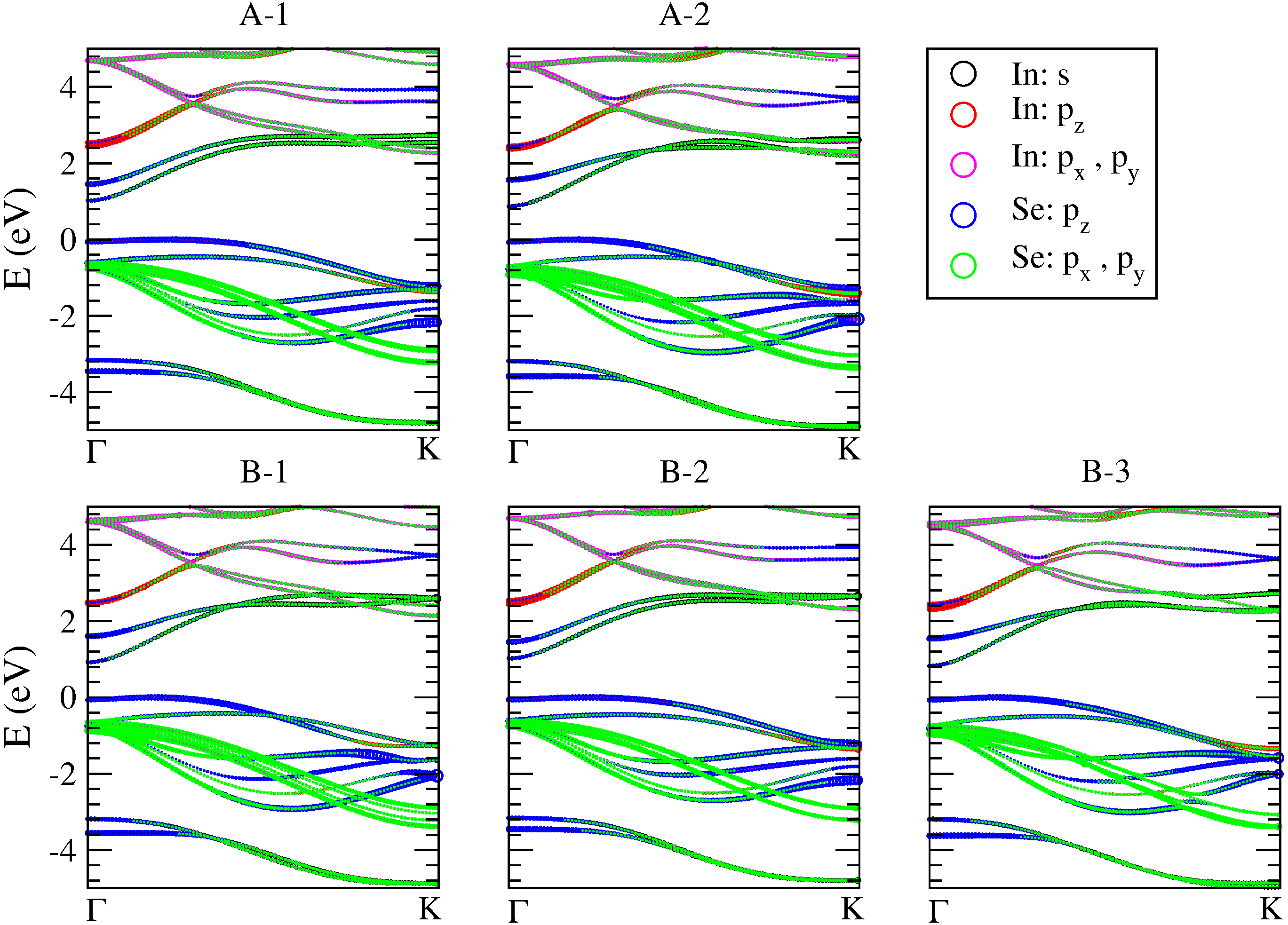
Fig. S3 shows the various band structures of twisted InSe monolayers along to K of the untwisted (0o) InSe monolayer. The band structures remain almost the same from to the highest energy kpoint of the VBM (the kpoint we concern) for various twist angles. It suggests that the band gap and the effective mass for holes are not affected by the variation of kpoint path at different twist angles.
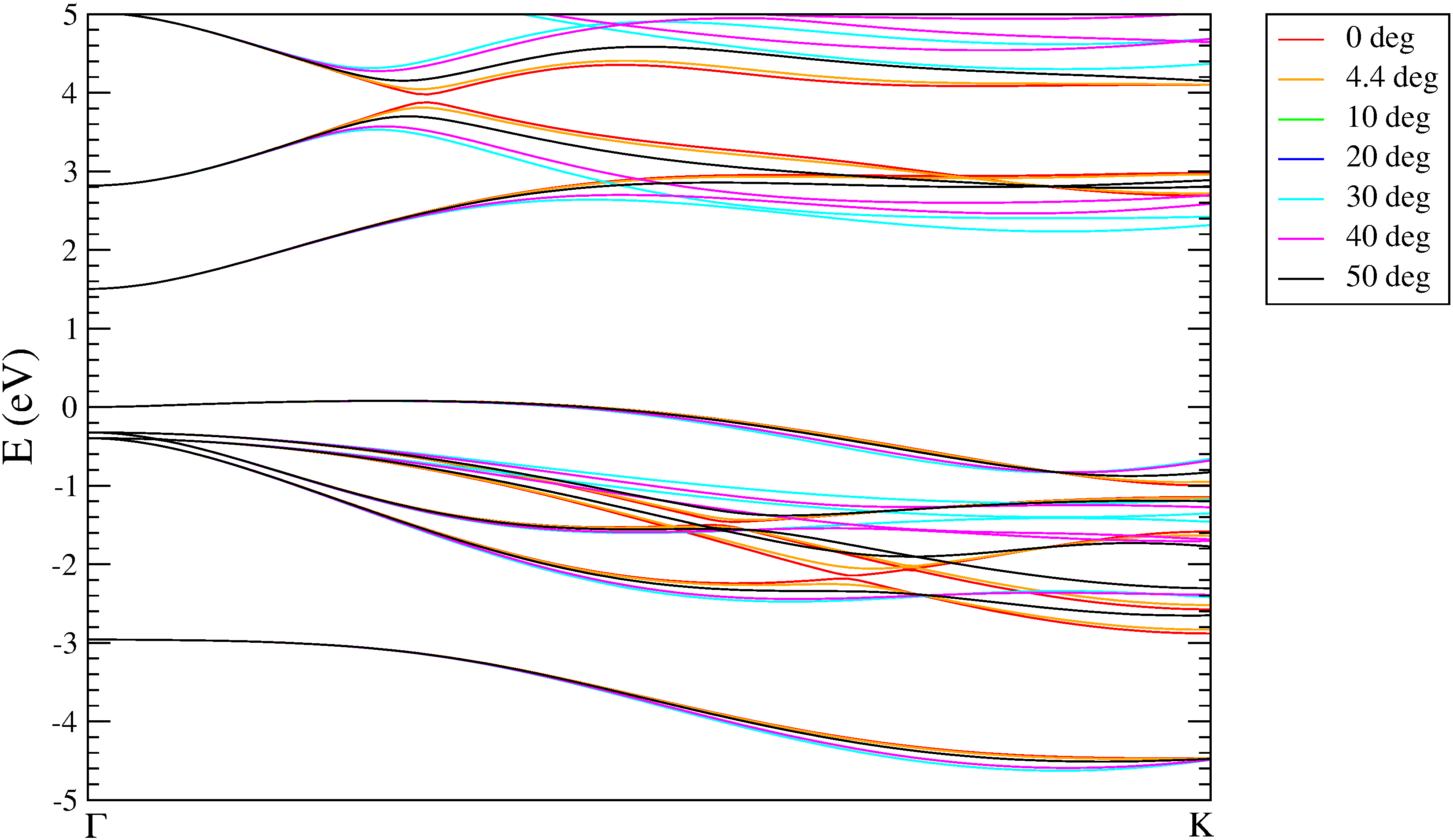
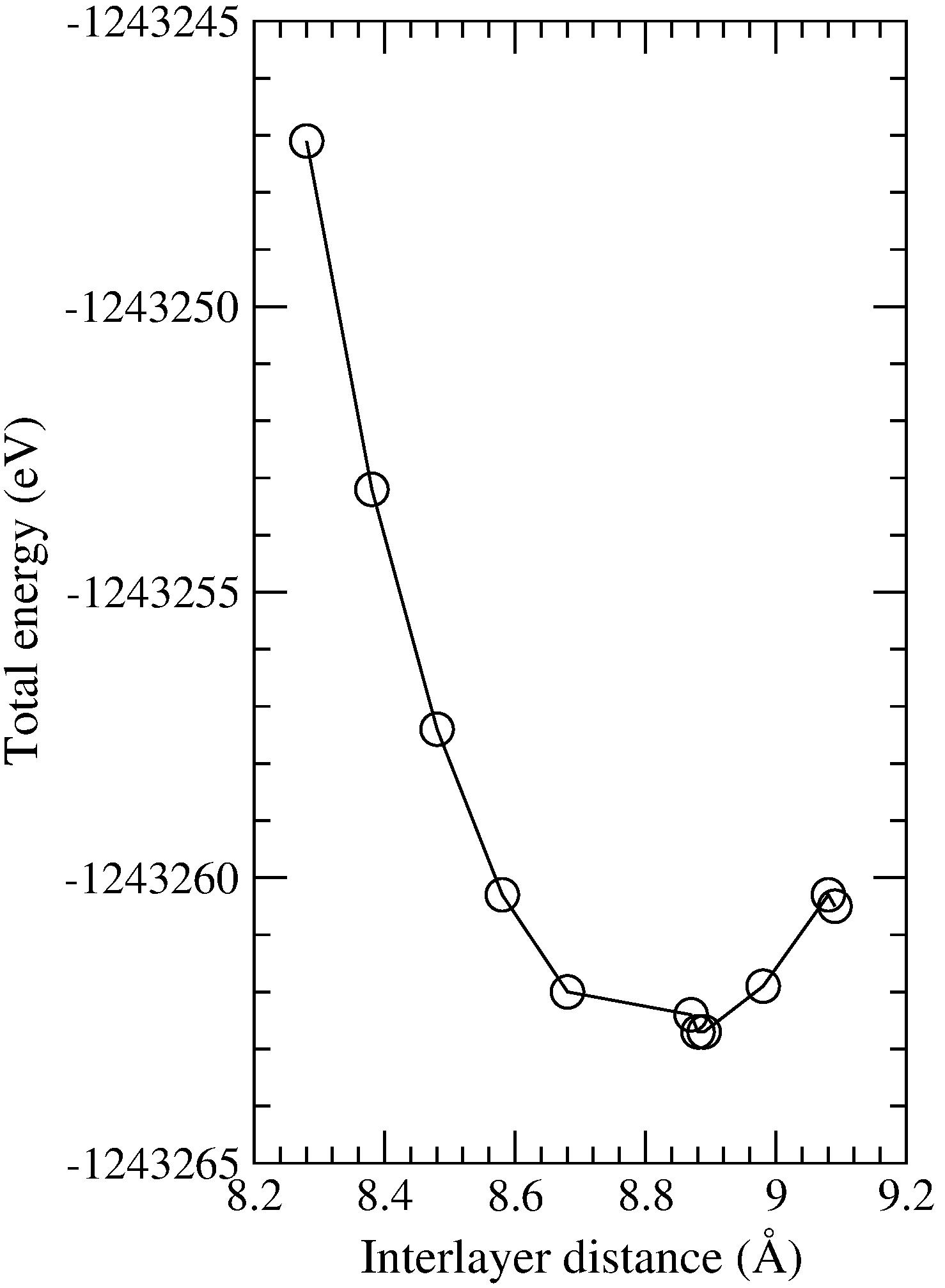
Fig. S4(a) shows the total energy versus interlayer distance for the A-type twisted InSe bilayer with a twist angle of 4.4o. The interlayer distance is optimised to be 8.89 Å. The small corrugation ( 0.1 Å) is obtained at the optimised interlayer distance (d= 8.88 Å and d= 8.89 Å). In contrast, a larger corrugation ( 0.3 Å) is obtained if deviating from the optimised interlayer distance (d= 9.05 Å and d= 9.25 Å). According to the previous literature [13], the averaged corrugation in this work is defined as
| (5) |
where and are the averaged interlayer distance calculated from each In and Se sublayers in the top layer to the same sublayer in the bottom layer when including out-of-plane corrugation and the optimised interlayer distance without including out-of-plane corrugation, respectively.
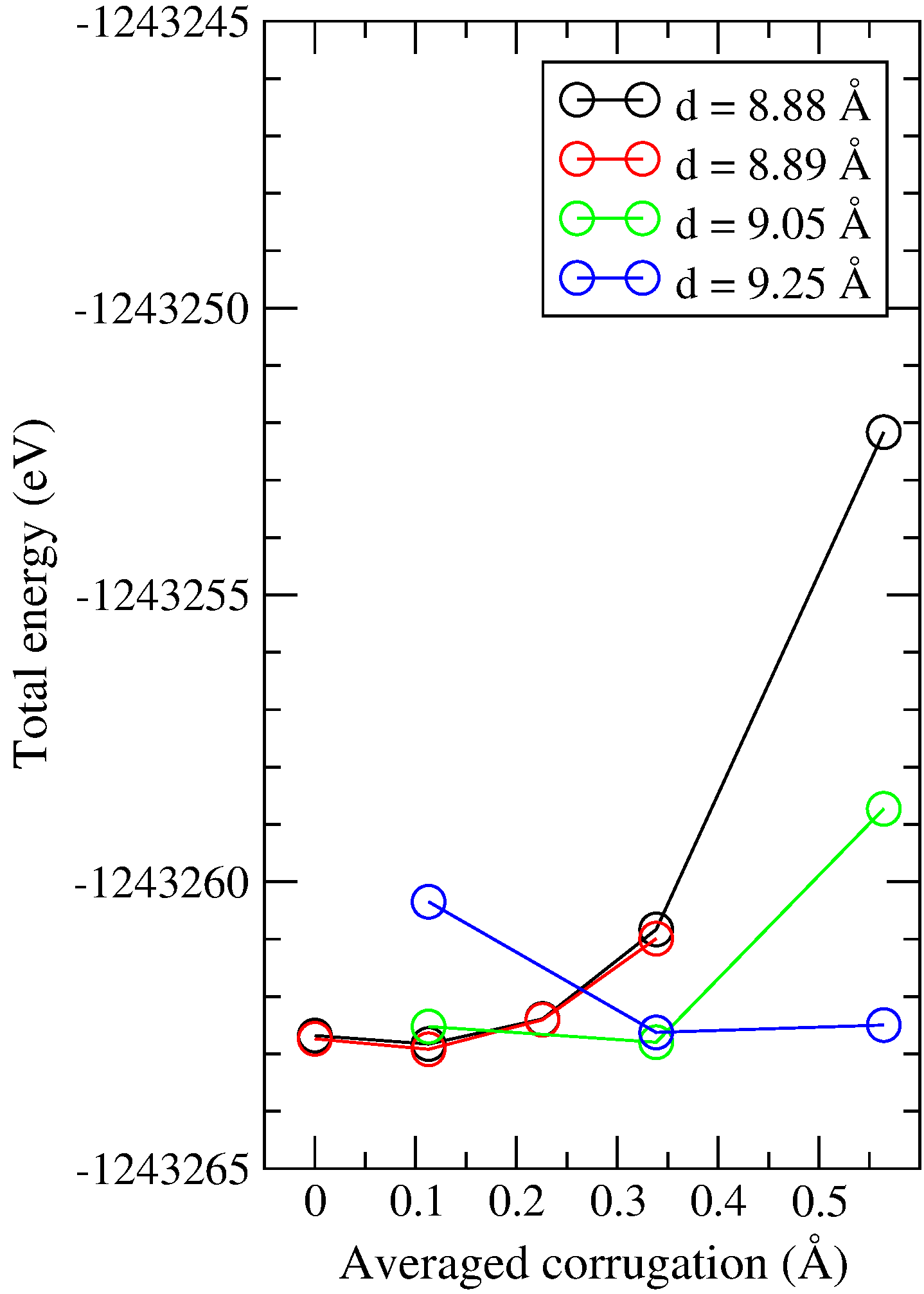
The effective band structure with the consideration of the corrugation looks similar to the effective band structure without consideration of the corrugation. The separation between neighbouring bands such as the VBM and the band below it slightly increases by the corrugation.


An initial atomic structure was given according to the distribution of the interlayer distance corresponding to different stacking configurations seen in some regions of twisted InSe bilayer (see table 1). Fig. S6 shows an initial atomic structure with the consideration of the averaged corrugation ( 0.1 Å) for the A-type twisted InSe bilayer with a twist angle of 4.4o.
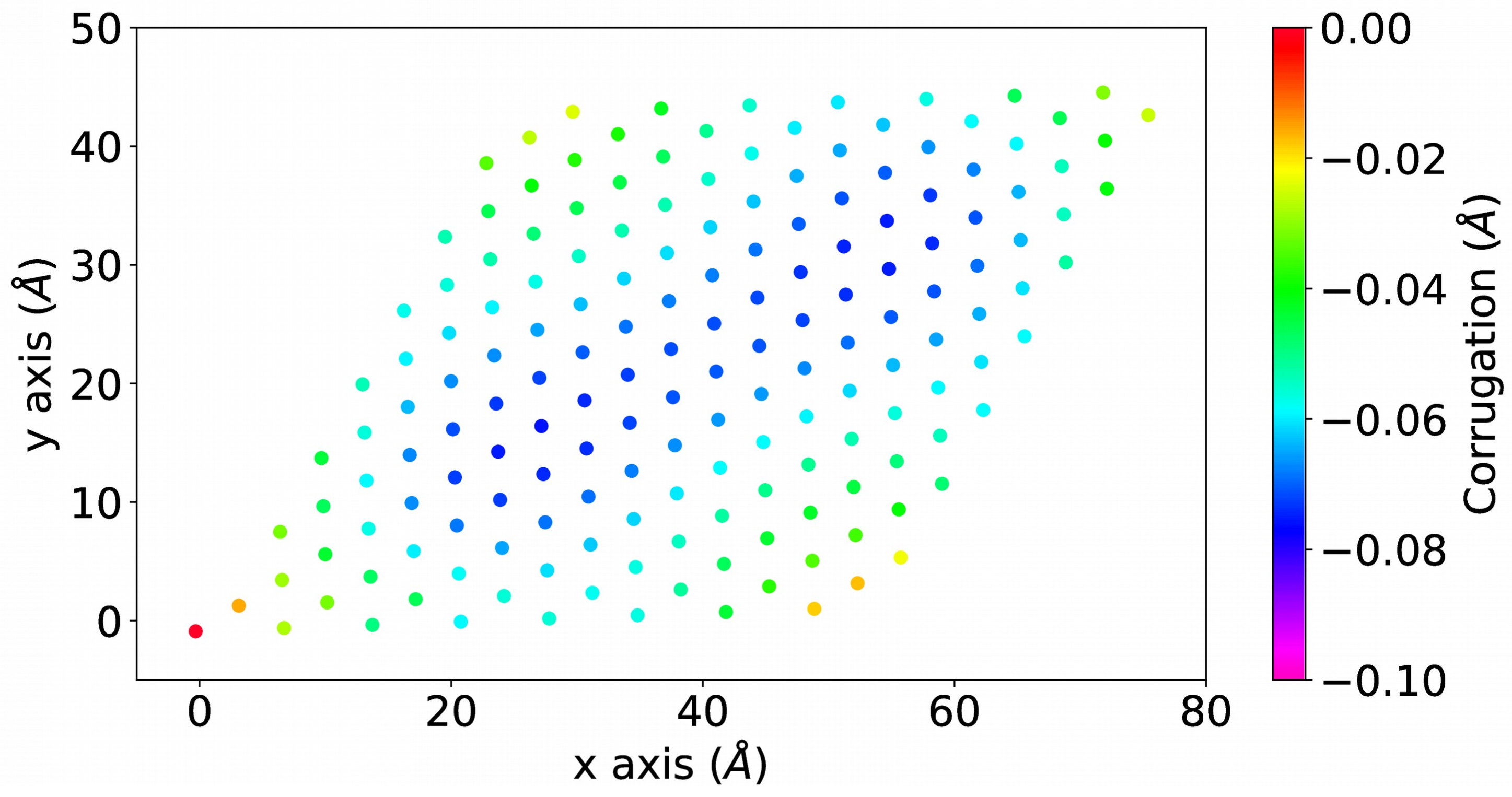
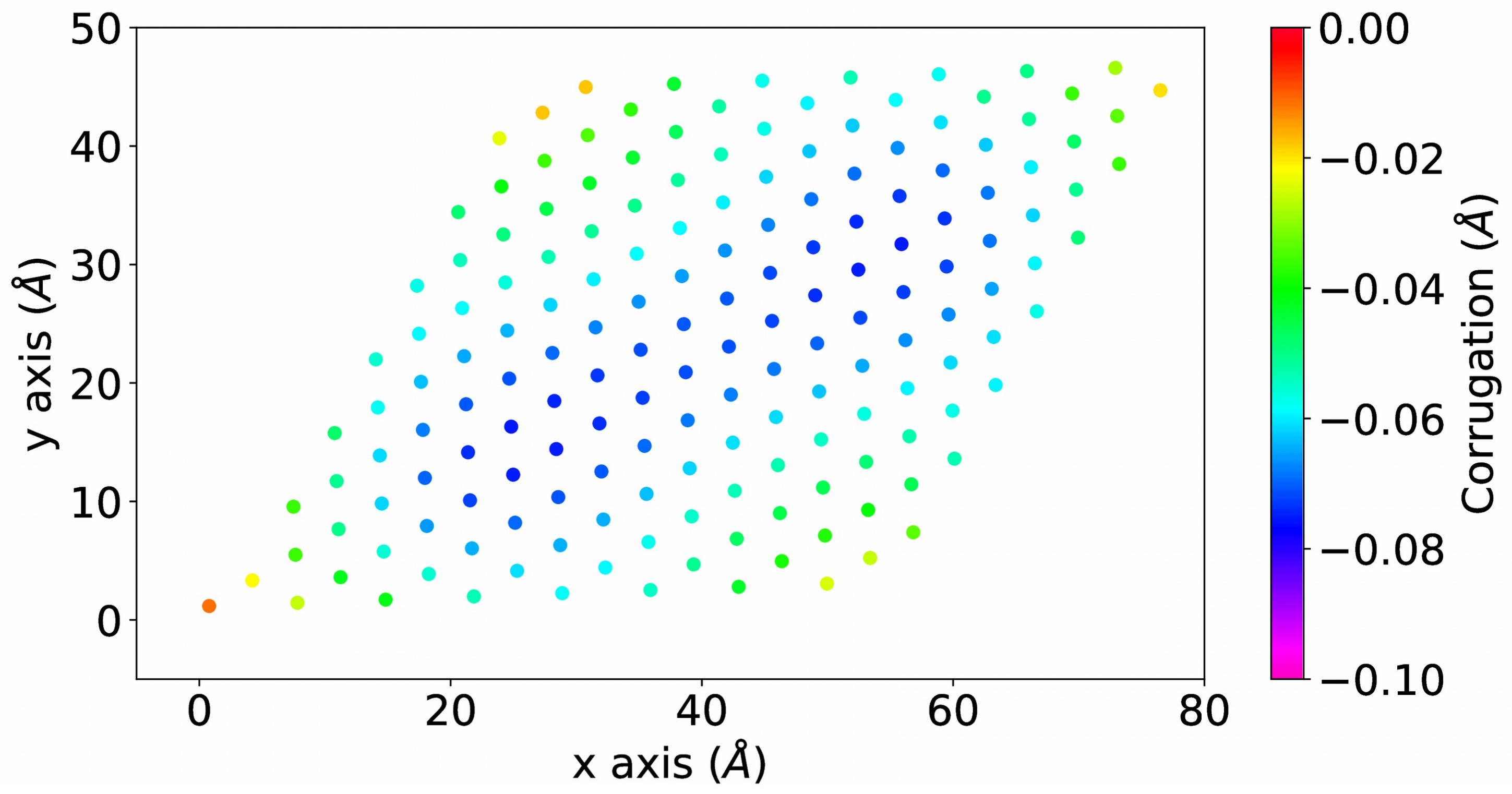
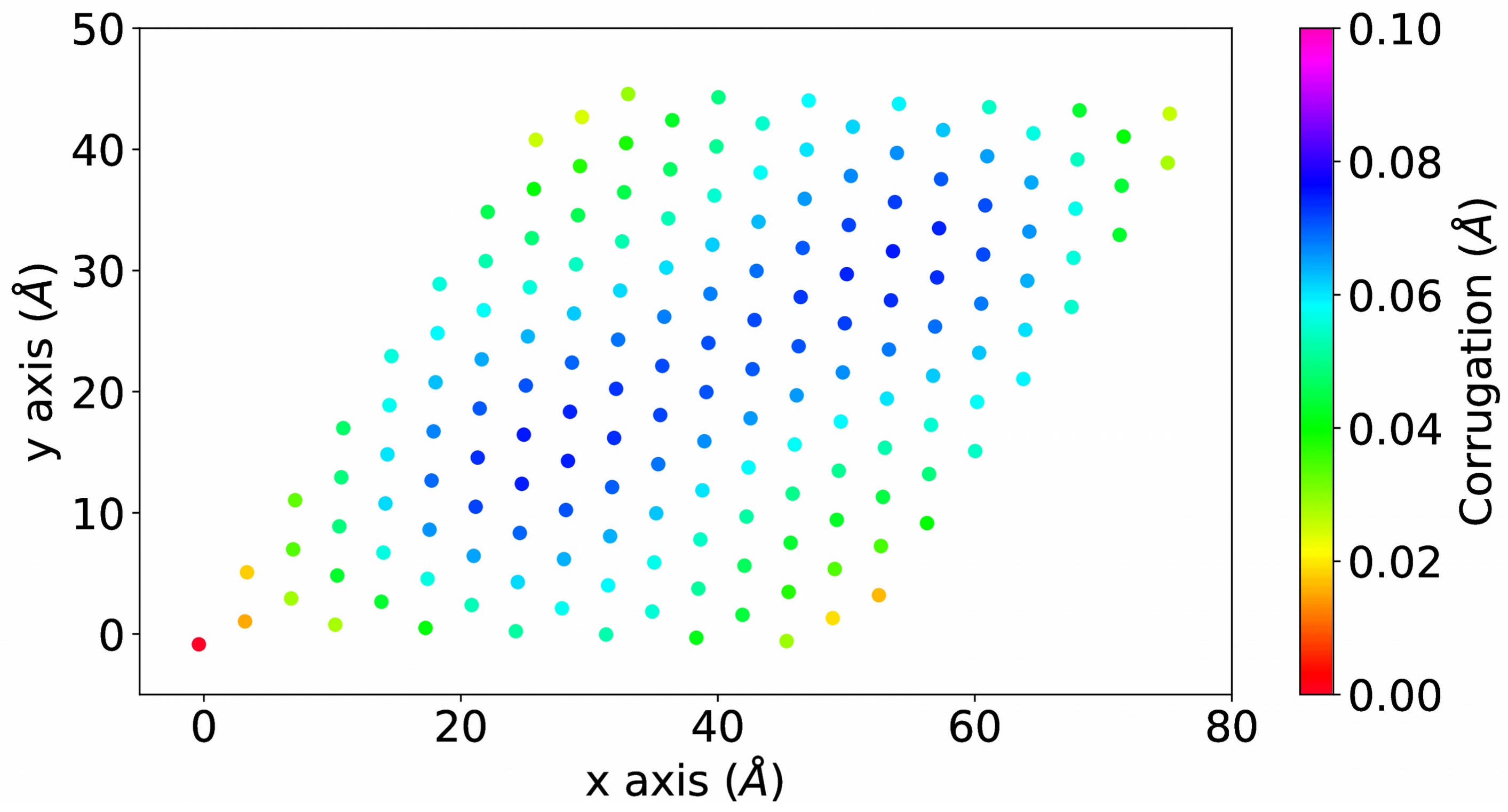
Before structural relaxation, the innermost In atoms (Inbt and Intb) do not show a similar distribution of the residual total force to the neighbouring Se atoms (Sebt and Setb).
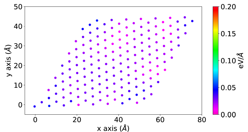
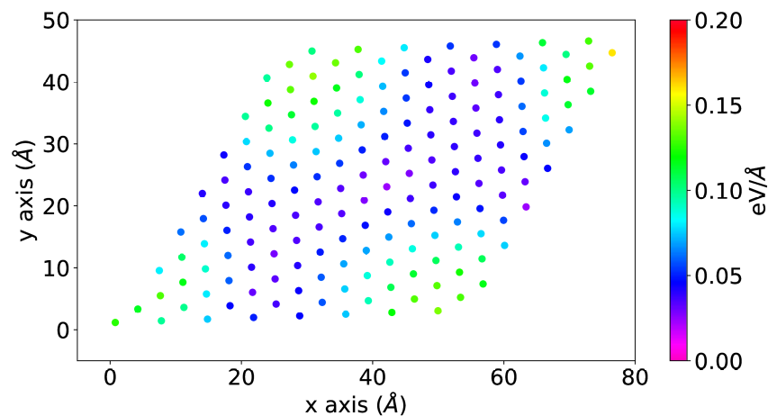

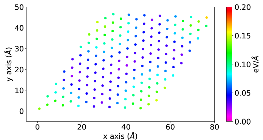
After the structural relaxation, the similarity between fig. 5 and fig. S6 is remained for the residual force in the z direction. The distribution is similar for the neigbouring In and Se atoms, whereas the residual force is larger in Se atoms. The z direction of the residual force is opposite in the top and bottom InSe layers. The total residual forces mostly originate from the residual forces along the z direction.
After the structural relaxation, the similarity between fig. 5 and fig. S6 is remained for the residual force in xy plane. The distribution is similar for the neigbouring In and Se atoms, whereas the residual force in the xy plane is larger in Se atoms.
The effective band structures of InSe monolayer, the A-type twisted InSe bilayer and the hBN-encapsulated A-type twisted InSe bilayer with a twist angle of 4.4o are shown in fig. S10. The inclusion of spin-orbit coupling in the calculation leads to the band splittings. The splitting of the VBM is only slightly pronounced near K for these three different systems.
The effective band structures of the B-type twisted InSe bilayers with twist angles of 4.4o, 17.9o and 27.8o are shown in fig. S11. The inclusion of spin-orbit coupling in the calculation leads to the band splittings. The splitting of the VBM is only slightly pronounced near K for these three different systems.
The hBN layer does not affect the VBM of twisted InSe layers in the hBN-encapsulated twisted InSe bilayer because the energy difference between the VBM of the hBN layer and the VBM of twisted InSe bilayer is at least 1.5 eV (see fig. S12 and fig. S13).
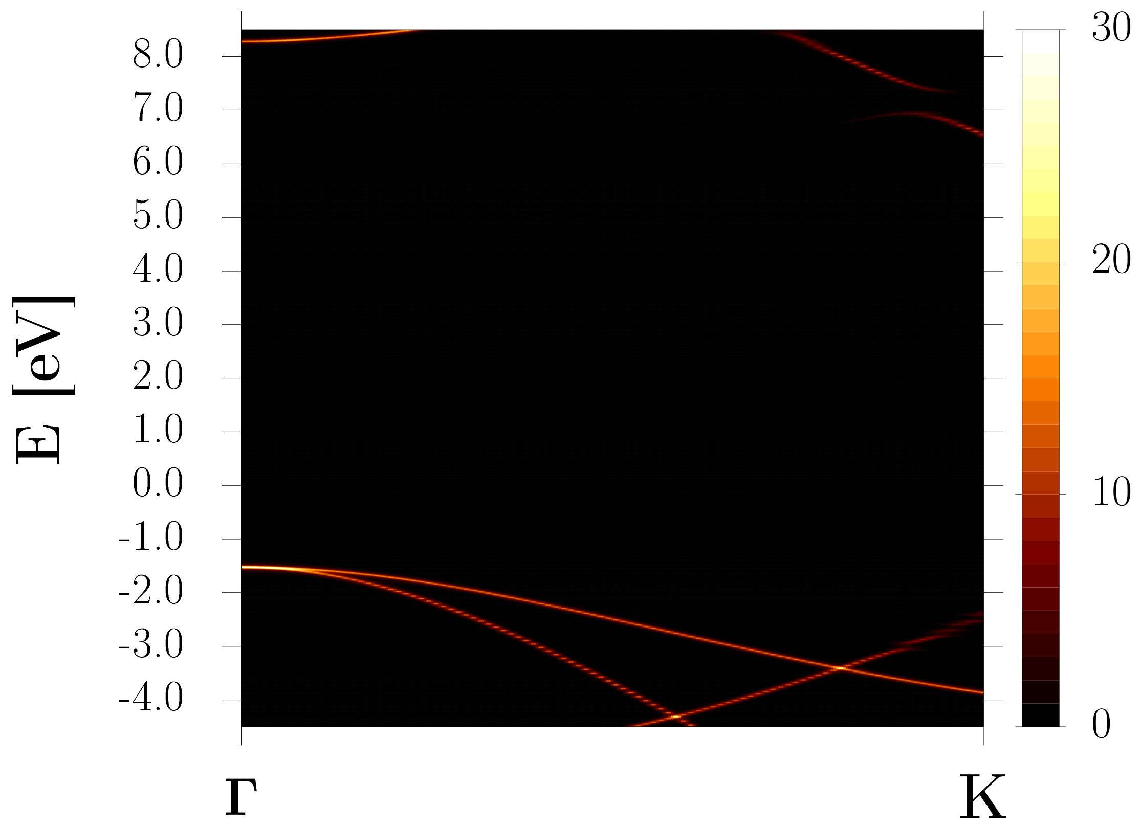
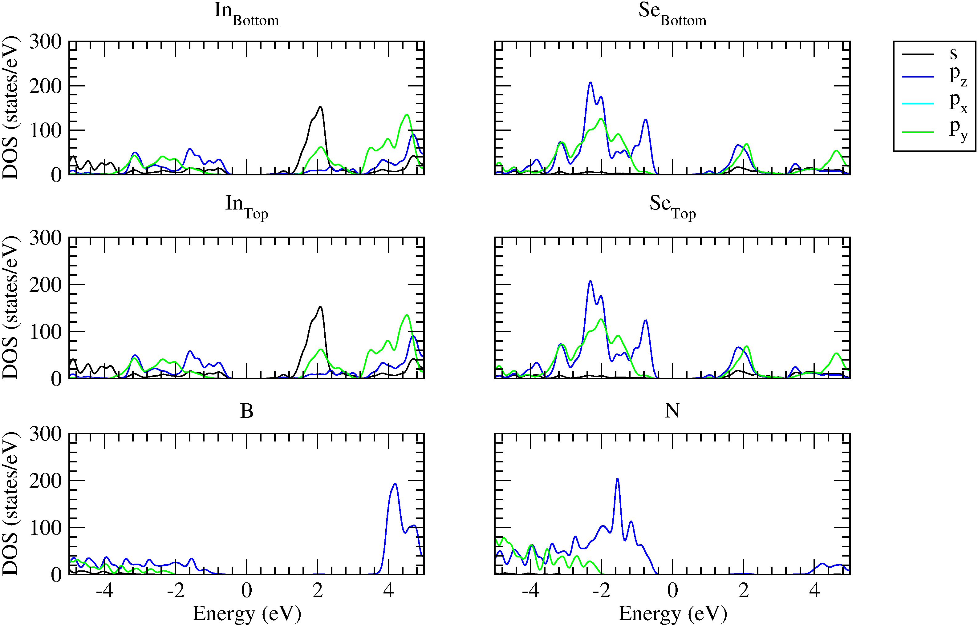
Fig. S14 shows the effective band structures of the A-type twisted InSe bilayer and the hBN-encapsulated A-type twisted InSe bilayer with a twist angle of 4.4o projected on the bottom and top InSe layers along to K of the bottom layer. The difference of the VBM between the bottom and top layers increases near K as the twist angle increases (see also fig. S3).

the bottom layer) (= 4.4o)

the top layer) (= 4.4o)

the bottom layer) (= 17.9o)

the top layer) (= 17.9o)
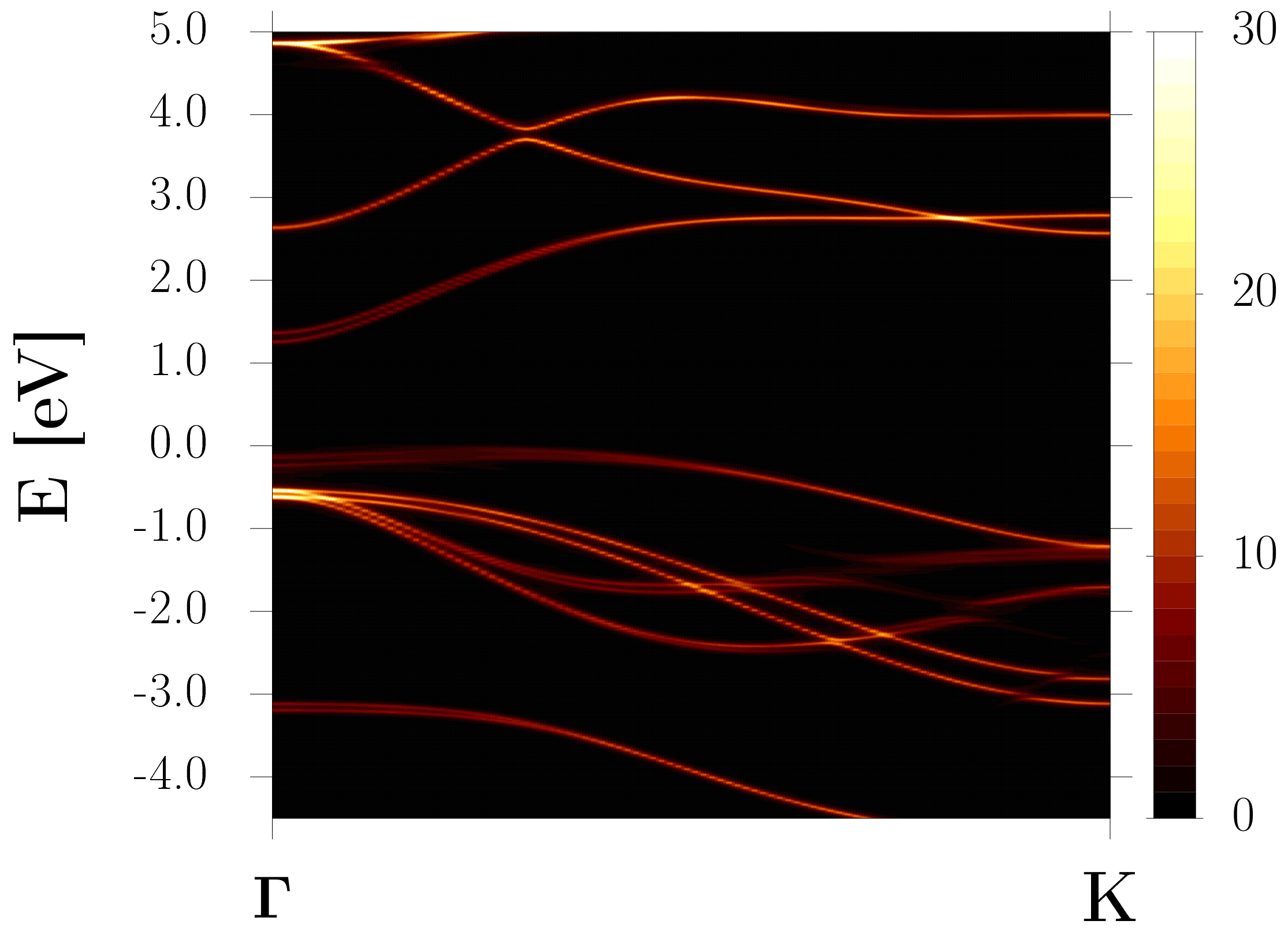

Fig. S15 shows the effective band structures of the B-type twisted InSe bilayers with twist angles of 4.4o, 17.9o and 27.8o projected on the bottom and top InSe layers along to K of the bottom layer. The difference of the VBM between the bottom and top layers increases near K as the twist angle increases (see also fig. S3).
the bottom layer)

the top layer)

the bottom layer)
the top layer)

the bottom layer)
the top layer)
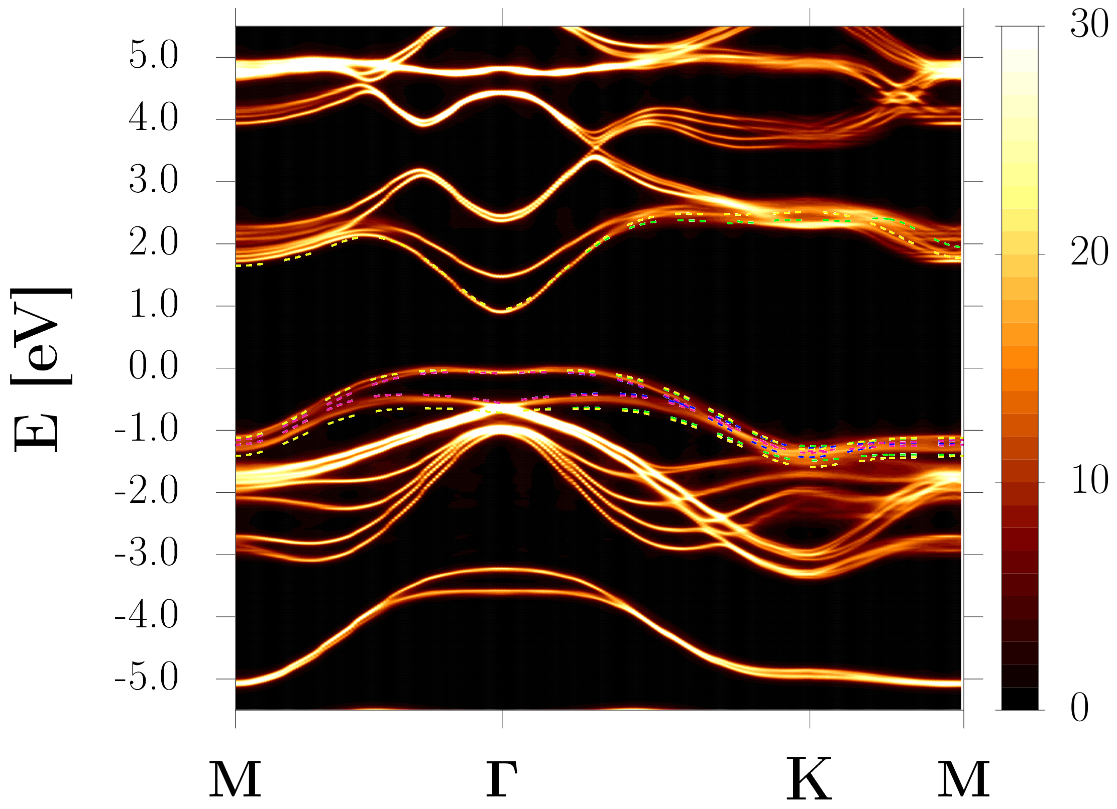
Fig. S17 shows the effective band structure of the A-type and B-type twisted InSe bilayers with different twist angles. The contribution of bands from the top InSe layer becomes obvious as the twist angle increases.

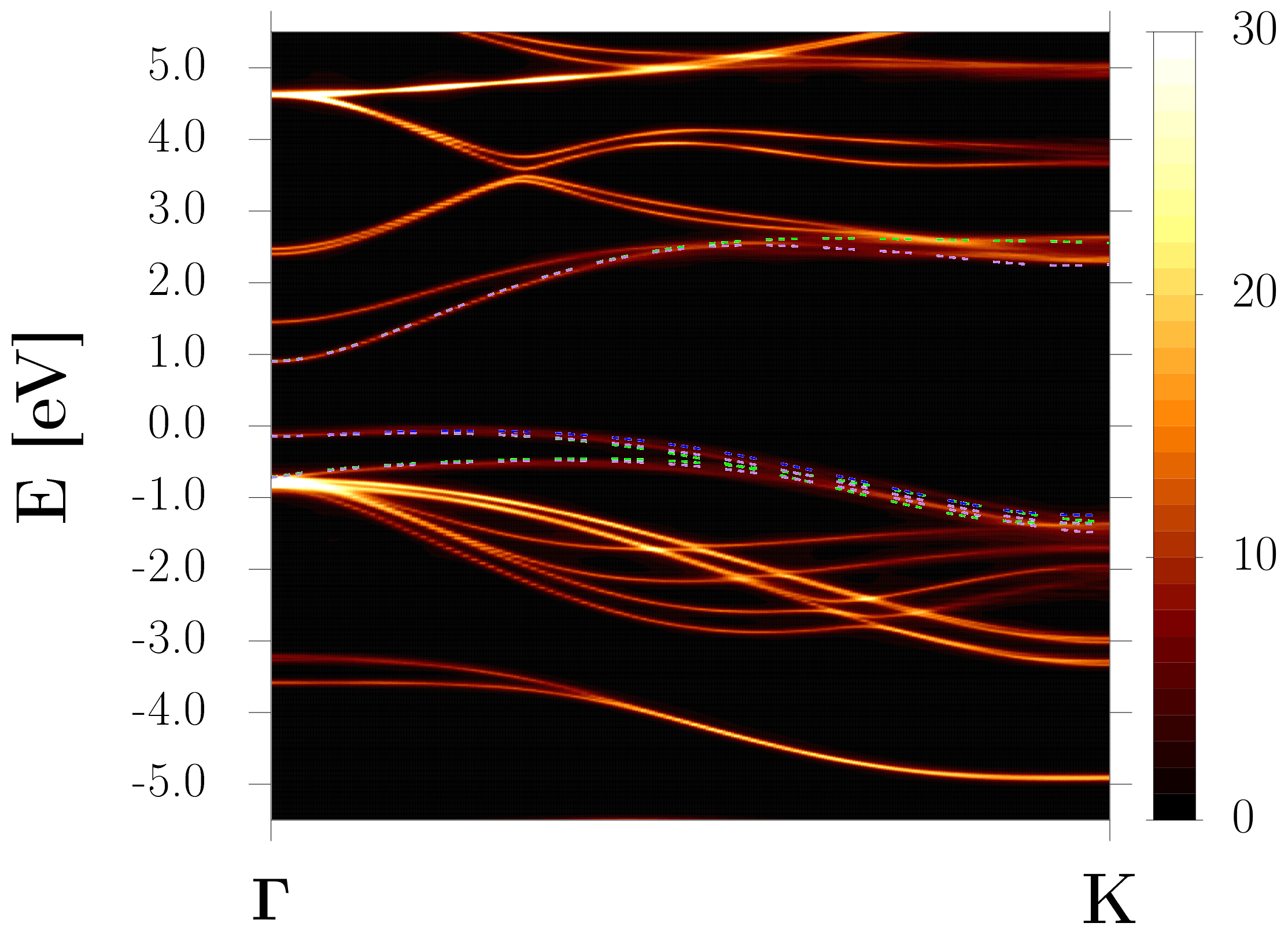


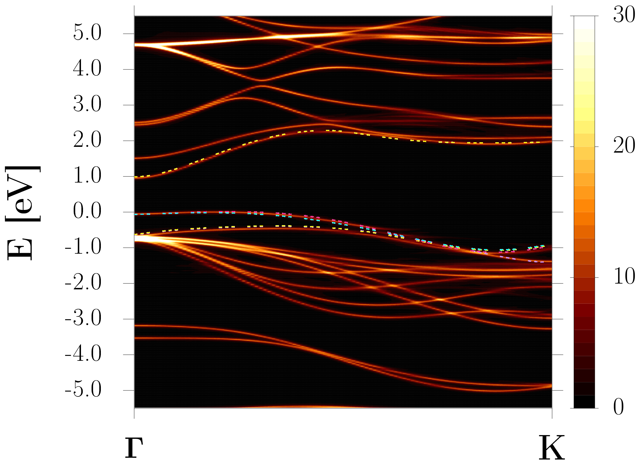
Fig. S18 shows the comparison of the VBM and the band below it between two different lattice constants for the A-2 stacking. 4.059 Å is the lattice constant for twisted InSe bilayer, whereas 4.063 Å is the lattice constant for the A-2 stacking. It shows that the difference of the VBM and the band below it between these two lattice constants is very small. We can ignore the effect of the lattice constant for different stacking configurations seen in some regions of twisted InSe layer when using 4.059 Å as the lattice constant of twisted InSe bilayer.
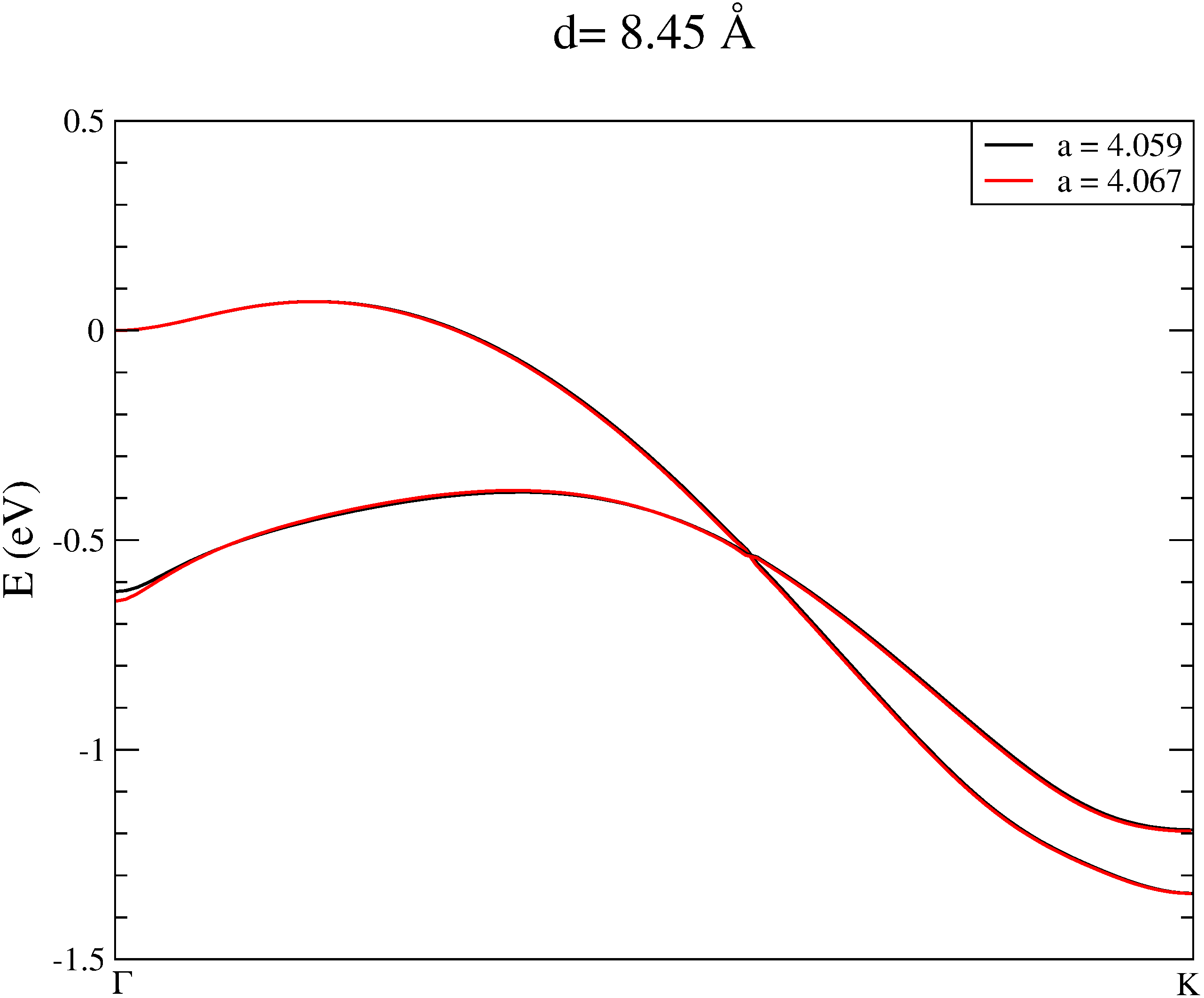
Fig. S19 shows the comparison of the VBM and the band below it between two different interlayer distances for the A-type and B-type stacking configurations. One of the interlayer distances is the optimised interlayer distance for InSe bilayer with each type stacking configuration, the other is the optimised interlayer distance for twisted InSe bilayer with a twist angle of 4.4o. The interlayer distances for the A-type and B-type twisted InSe bilayers with a twist angle of 4.4o are 8.89 Å and 8.82 Å, respectively (see also table 1). The flatter VBM at the highest energy kpoint (red curve) associated with a larger interlayer distance, which means the effective mass for holes is larger with a larger interlayer distance (consistent with table 1). The VBM and the band below is getting closer with increasing interlayer distance because of the weakening of the repulsion between these two bands.
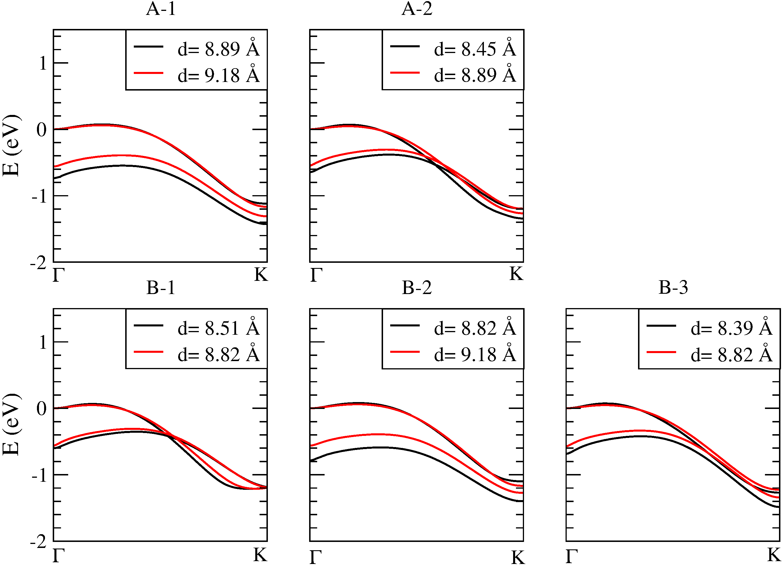
Figure S20 shows the interlayer distance versus the twist angle for twisted InSe bilayer. For the twist angles considered in this work, the interlayer distances are 8.850.04 Å.
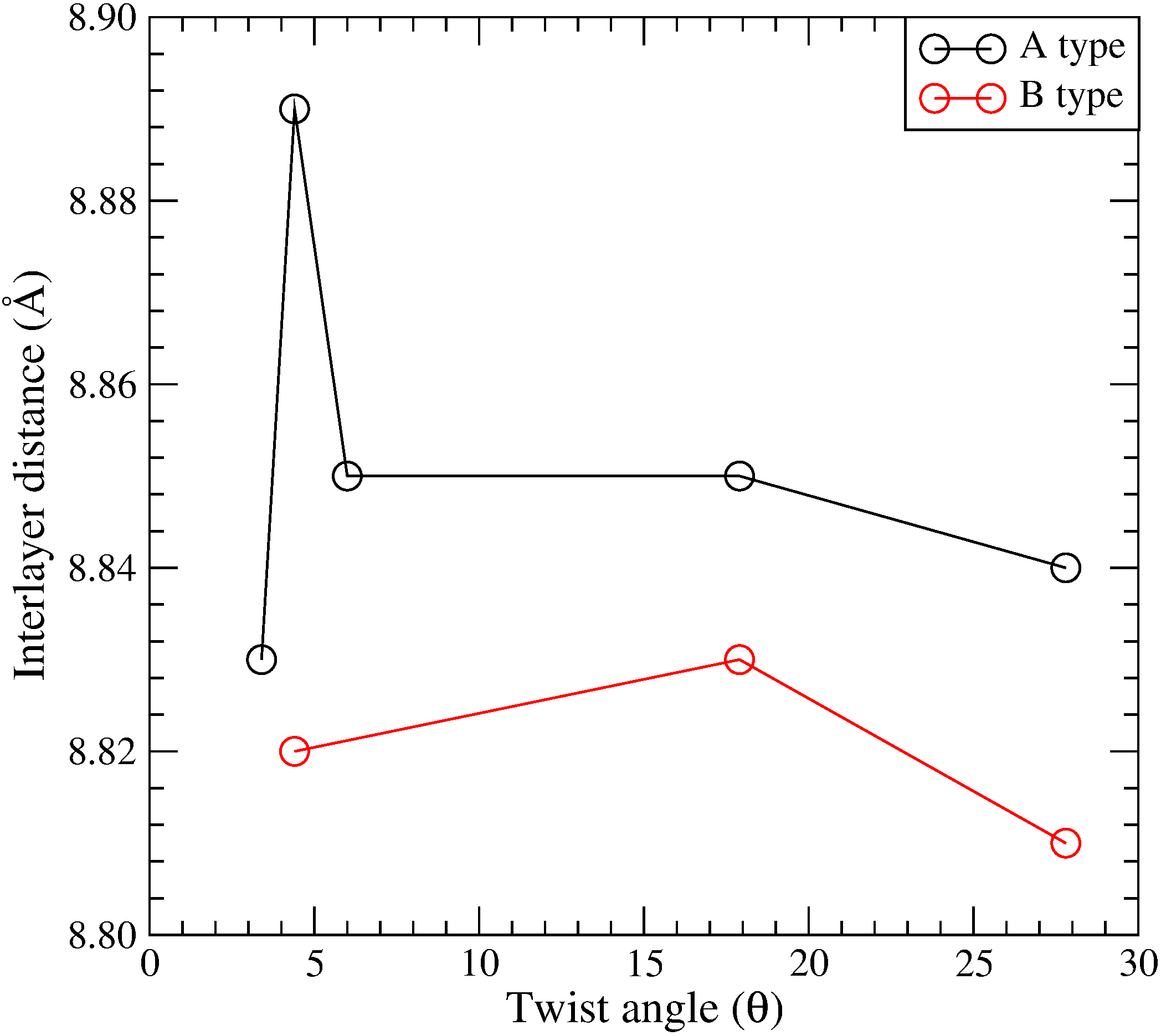
Figure S21 shows the VBM and the band below it for InSe bilayers with different stacking configurations at different interlayer distances and twist angles. The difference of the effective mass for holes calculated around the highest energy kpoint of the VBM is very small for different twist angles considered in this work.
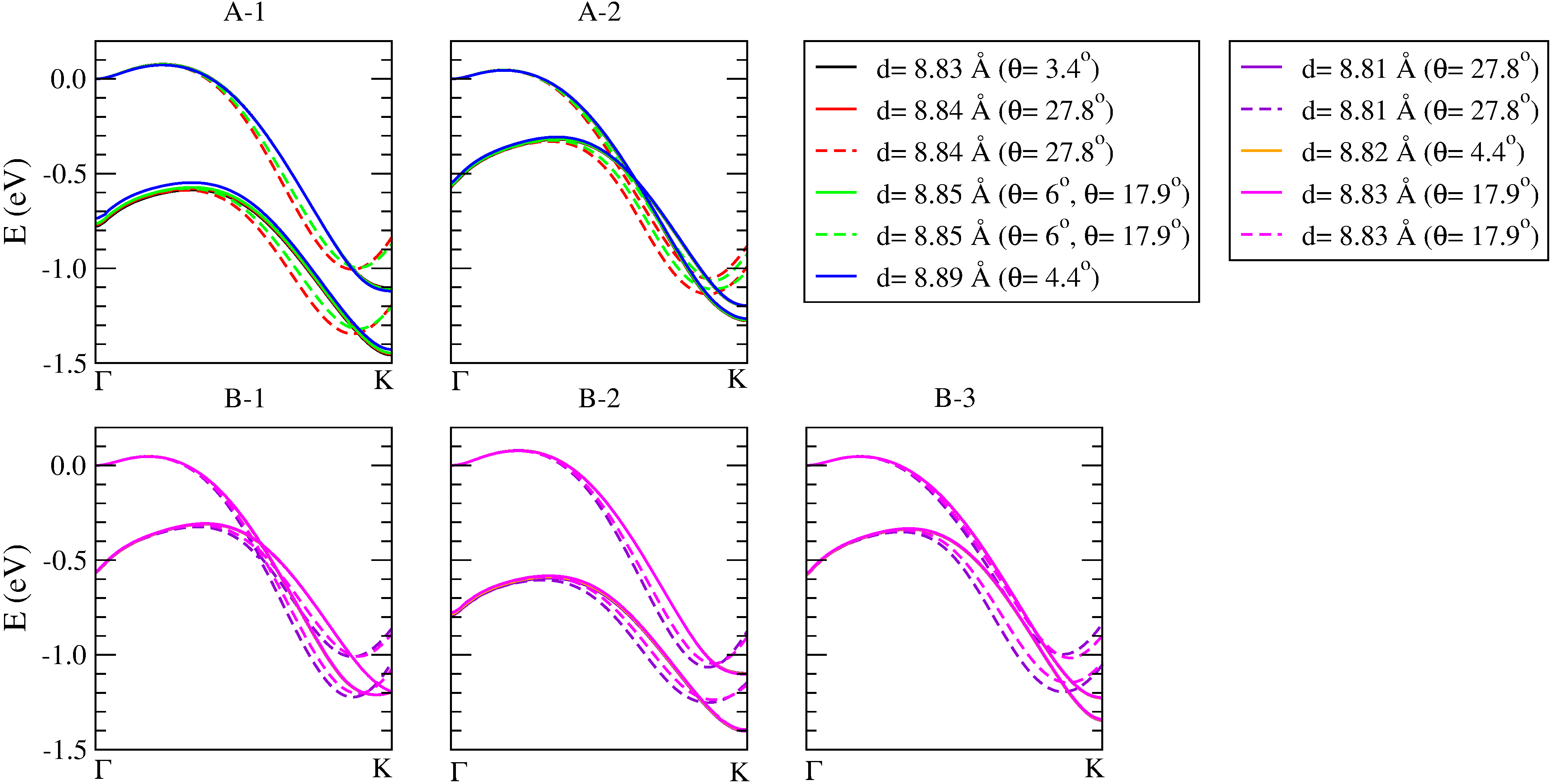
Fig. S22 shows the superposition of the VBM and the CBM in InSe monolayer from the primitive cell calculations (purpe curves) on the effective band structure of the hBN-encapsulated A-type and B-type twisted InSe bilayers from the supercell calculations. These bands from the primitive cell calculation match well with the same bands in the effective band structures from the supercell calculations for both the hBN-encapsulated A-type and B-type twisted InSe bilayers. This further verifies the argument that the insertion of the hBN layer causing the separation of two InSe layers.

9 Calculation of exciton binding energy
According to the previous literature [39, 45, 46], the intralayer and interlayer exciton binding energies are calculated as following procedure. The Hamiltonian of the system is
| (6) |
with and
| (7) |
can be any values and (, ) is within the range of possible exciton Bohr radius. The Hamiltonian problem becomes
| (8) |
with in analytical form and , where in analytical form is
| (9) |
and . With different , can refer to intralayer or interlayer potential energy matrix elements with considering the screening effect from other layer. can be obtained from the Rytova-Keldysh potential (: zeroth Struve functions and : zeroth Bessel functions of the second kind).
| (10) |
| (11) |
| (12) |
The definition of parameters are ( is the interlayer distance), ( is the dielectric constant of environment) and ( is the in-plane polarizability) for the screening length.
Furthermore, the intralayer exciton binding energy of twisted InSe/hBN/InSe can be calculated according to the Coulomb potential for the monolayer in analytical form below:
| (13) | ||||