Insights into electron transport in a ferroelectric tunnel junction
Abstract
The success of a ferroelectric tunnel junction (FTJ) depends on the asymmetry of electron tunneling as given by the tunneling electroresistance (TER) effect. This characteristic is mainly assessed considering three transport mechanisms: direct tunneling, thermionic emission, and Fowler-Nordheim tunneling. Here, by analyzing the effect of temperature on TER, we show that taking into account only these mechanisms may not be enough in order to fully characterize the performance of FTJ devices. We approach the electron tunneling in FTJ with the non-equilibrium Green function (NEGF) method, which is able to overcome the limitations affecting the three mechanisms mentioned above. We bring evidence that the performance of FTJs is also affected by temperature, in a non-trivial way, via resonance (Gamow-Siegert) states, which are present in the electron transmission probability and are usually situated above the barrier. Although the NEGF technique does not provide direct access to the wavefunctions, we show that, for single-band transport, one can find the wavefunction at any given energy and in particular at resonant energies in the system.
I Introduction
The asymmetric ferroelectric tunnel junction (FTJ), a thin ferroelectric (FE) film sandwiched between two dissimilar metallic electrodes or with different interfaces in the case of the same electrode material(Fig. 1), is a promising electron device for many applications such as low power memories [1] or neuromorphic computing [2]. The salient mechanism of FTJ is based on the tunneling electroresistance (TER) effect, i. e., a change in the electrical resistivity when the electric polarization is reversed under external electric field [3, 4]. In other words, the electrical resistance of FTJ switches from a high conduction (ON) state to the low conduction (OFF) state or vice-versa when a high voltage pulse is applied. Ferroelectrics like BaTiO3, PbZr0.2Ti0.8O3, BiFeO3 [5, 6, 7] as well as high-k dielectrics like HfO2, Hf0.5Zr0.5O2 [8, 9] have been shown to work as FTJs. The latter are particularly attractive since they a compatible with CMOS technology.
The TER effect that is based modulation of the barrier potential upon the polarization reversing can be characterized the TER ratio
| (1) |
where are current densities in the two different states. The higher the TER ratio and the , the better is the FTJ performance. The extent of barrier modulation depends on numerous factors, such as: i) the thickness and spontaneous polarization of the ferroelectric film, ii) the bias voltage, iii) the difference between work functions and also between screening lengths of electrodes, iv) the built-in field and screening of the polarization charge, as well as the variation of barrier thickness due to piezoelectricity [10].
To understand, describe, and model the TER effect, the ab-intio methods may provide an accurate image of the physics governing FTJ systems like the geometry, polarization, electronic structure [11], and transport properties [12, 13]. Nevertheless,ab-initio methods require large computational resources, which may prevent their intensive use in the early stages of FTJ design, when there is a requirement of a quite fast scan in parameter space to obtain a device with required functionalities. In the search of optimized devices, the semi-empirical methods are fast and, despite all simplifications, are extremely useful for the treatment of the charge transport as long as they are fed with appropriate physical parameters [14, 15]. These semi-empirical methods are based on the non-equilibrium Green function (NEGF) method that can calculate exactly, in principles, the tunneling current and the I-V characteristic in an FTJ [15].
In semi-empirical methods based on NEGF the parameters can be adjusted to match the experimental data [14]. In many cases, in order to characterize the electron transport in FTJs and interpret the I-V curves, various models of transport mechanisms involving direct tunneling, thermionic emission, and Fowler-Nordheim tunneling are used [16]. Direct tunneling presumes low energy for incident electrons such that tunneling probability doesn’t depend on the profile of the barrier, which is assumed to be rectangular on average in the case of Simmons formula [17, 18] or trapezoidal in the case of Brinkman et al. formula [18, 19]. Thermionic emission is that part of the current carried over the top of the barrier by thermally activated charge carriers [20]. The last mechanism, the Fowler-Nordheim tunneling, is used for triangular barrier profiles which are encountered at finite applied bias voltages [21]. The treatment of the above mechanisms is based on some approximations for electron transport. Simmons and Brinkman et al. as well as the Fowler-Nordheim formulae are based on the semi-classical WKB approximation [17, 21], while thermionic emission tacitly assumes a homogeneous transmission probability of one for all electrons with energy above the top of the barrier [20].

In this work, by the exact treatment of the tunneling within the NEGF method, we show that the above models describing direct tunneling, thermionic emission, and Fowler-Nordheim tunneling are not accurate enough for performance characterization of the FTJs. These models cannot capture resonant features emerging in FTJ structures that might play an important role in carrier transport and ultimately in the performances of device. The electric current of an impinging electron at a given energy is determined by the electron transmission probability at that energy weighted (multiplied) by its Fermi-Dirac distribution function. Hence, even though they seem unlikely to play a role in the tunneling due to relative simple structure of the barriers, the resonances can contribute significantly to the electric current since their contribution to transmission probability may offset temperature-dependent Fermi-Dirac factor. In the following we will show that the resonances emerging close or above the top of the barriers play a decisive role for transport at room temperature, fact that is not captured by the simple models previously mentioned. Moreover, resonances may appear in composite (both a ferroelectric and a dielectric) barriers. The NEGF method can accurately describe also these types of heterostructures. Generally, the NEGF approach cannot provide full access to the wavefunctions especially for multi-band transport [22], however for a single-band transport we show that this is not the case, the eigenvectors of the spectral functions are just the wavefunctions of the system. At this stage we are able to identify the Green function of the device as the discrete version of the outgoing Green function which is used in diverse scattering problems like nuclear reactions [23] or electron transport in nanostructures [23, 24]. The advantage of such correspondence is that the NEGF of the device and the transmission probability can be expanded as a sum of resonance or Gamow-Siegert states [23, 24, 25, 26]. Thus we are able to sort out the resonances that count for the electron transport in FTJs.
The paper is organized as follows. The next section deals with the theoretical background: the calculation of polarization induced electrostatic potential across the FTJ, the calculation of transport quantities like I-V curve and conductance by NEGF method, and the evaluation of wavefunctions and resonance states from NEGF calculations. The third section presents numerical results regarding the effect of temperature on electric conductance and TER ratio for several practical cases of simple or composite BaTiO3 based FTJs. In addition, the wavefunctions and resonance states for such FTJ structures are analyzed. The fourth section summarizes the conclusions of this work. Lastly, in the Appendix we present the steps to obtain a discrete tight-binding Hamiltonian from the BenDaniel and Duke Hamiltonian [22].
II Theoretical background
II.1 The profile of potential barrier
In semi-empirical methods the calculation of tunneling current and electric conductance is performed by solving simultaneously the electrostatic and transport problems They are intricately interrelated since the charge density in Poisson equation is calculated self-consistently from the NEGFs [22]. However, when one deals with free carriers only in the metallic contacts they can decouple each other. So, let us first deal with the electrostatics and the profile of the barrier potential. In the following we treat the composite FTJ, where the barrier is composed of a dielectric and a ferroelectric layer. If the thickness of dielectric is fixed to and that of the ferroelectric to , we assume that the dielectric and ferroelectric are located for between - and 0 and for between 0 and , respectively, while the metallic contact ML is at and the metallic contact MR is at . A widely used and good approximation of the electrostatics in metals is the Thomas-Fermi approximation [14, 27]. Within this framework, the electrical fields in ML and MR are given by
| (2) |
| (3) |
In Eqs (2) and (3) S is the screening charge at ML/dielectric and ferroelectric/MR interfaces, 1( and 2( are the Thomas-Fermi screening lengths (dielectric constants) of ML and MR, respectively, and 0 is the vacuum permittivity. In the following we respectively denote by FE, , and the dielectric constant, the electric field, and the intrinsic polarization of ferroelectric and by , DE the electric field and the dielectric constant of the dielectric. The electrostatic equations are in fact the continuity of the normal component of the electric induction at both ferroelectric/MR and ML/dielectric interfaces
| (4) |
Additionally, the bias voltage across the structure obeys the equation
| (5) |
where is the applied voltage and is the built-in voltage bias due to mismatch of the conduction bands (conduction band discontinuities) and of Fermi energies ( ) of ML(MR)
| (6) |
In Eq. (6) is the elementary electric charge, 1 is the band discontinuity at the first interface between ML and the dielectric, 2 is the band discontinuity at the second interface between the ferroelectric and MR, and C is the band discontinuity at the interface between the dielectric and ferroelectric when the ferroelectric is unpolarized. Eliminating and from Eqs. (4) and (5) we obtain the screening charge S
| (7) |
Now it is straightforward to obtain the electric potential and the barrier profile knowing that the electric field is homogeneous in both the dielectric and the ferroelectric
| (8) |
In Eq. (8) is considered positive when points from ML to MR and negative when it points the other way around.
II.2 Transport by NEGF
Transport properties like electric current density and conductance can be calculated by solving the Schrödinger equation with scattering boundary conditions, i. e., either an incoming wave from the left or from the right. For a single band, the equation is merely 1D with a BenDaniel and Duke Hamiltonian, where the effective mass of electrons can vary across the structure [22]:
| (9) |
In Eq. (9) it is assumed that the energy band is parabolic with an isotropic effective mass in each layer of the nanostructure, is the transverse wavevector (parallel to each interface), is the effective mass, and potential energy given by Eq. (8). Equation (9) can be discretized into 1D problem in a tight-binding representation [22]. The details are presented in the Appendix. The Hamiltonian in the matrix format has the following tridiagonal form
| (10) |
In this format one can easily see that the Hamiltonian has three parts: the semi-infinite left (L) and right (R) metallic electrodes and the device (D) that is defined by , an matrix. Both electrodes act as reservoirs, hence they have well defined chemical potentials and temperatures. We can define the retarded Green function ( of the system at energy as the inverse matrix of [( + i) - ], where = 0+. Similarly the advanced Green function is the inverse of [(E - i], i. e.,
| (11) |
In the NEGF method one eliminates the degrees of freedom of contacts by introducing self-energies into the projected Green functions of the device (D)
| (12) |
The self-energy has two components due to the coupling to the left and right contact. It replaces the boundary conditions that otherwise would be fulfilled by the construction of a Green function in the device region. The self-energy due to the left contact has the following expression:
| (13) |
where is the Green function of the semi-infinite left contact. Also, has a similar expression. Here, we notice that due to the fact that we deal with a nearest-neighbor tight-binding Hamiltonian, the self-energies and are matrices with just one non-zero element, the (1,1) element for and (, for . Thus the retarded Green function is
| (14) |
The poles of the device Green function are no longer real, an attribute of an open quantum system. Starting from Eq. (13), the calculation of involves the calculation of matrix element (0,0) of , which is the surface Green function of the left contact. Bearing in mind that and are the tight-binding parameters of the left contact and defining a longitudinal wavevector , the energy can be parameterized according to the single-band dispersion relation for the left contact . One can find that the matrix element (0,0) of is and [14, 22, 27]. The expression of is calculated with outgoing boundary condition [27], hence the self-energy is for this kind of boundary condition.
One can further define: (a) the spectral function , which also has a matrix form, whose diagonal is just local density of states up the 2 factor, and (b) the broadening function due to the coupling to the left and right contacts . Using the projection operator on the device one can show that the projection of the full spectral function on the device space is [28]
| (15) |
Moreover one can further show that partial spectral densities
| (16) |
are spectral densities due to incident Bloch waves that come respectively from the left (L) and from right (R) [28]. Thus contains information about both solutions of the scattering problem. Furthermore it can be shown that the current flow from an incident Bloch wave that comes from the left electrode into the right electrode is
| (17) |
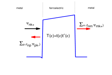
is just the matrix of transmission probability that has a schematic representation in Fig. 2. From Eq. (17) the expression of the total current takes the form of Landauer-Büttiker formula [15, 22]:
| (18) |
In Eq. (18) the Tr() operation includes both the trace over the matrix and the integration over the transverse wavevector k . The functions are the Fermi-Dirac distribution functions of the and electrodes. Performing the trace operation only over matrix we obtain the transmission probability coefficient and the the Landauer-Büttiker formula becomes
| (19) |
In addition, in the linear regime (small bias voltages and at temperature of 0K we obtain the Landauer conductance formula [15]
| (20) |
II.3 Retrieving the wavefunction from the spectral function. Resonance states
Let us consider the spectral function . It signifies the projected spectral function on the device for incident waves coming from the left. As it was pointed out in Ref. [28], in general the eigenvectors of cannot be identified with the wavefunction in the device region since there are several eigenvectors of with non-zero eigenvalues. This is rather obvious in the tight-binding representation but for multi-band problem. For a single-band problem, however, this is not the case. has just one non-zero eigenvalue. Its corresponding eigenvector is just the function that is proportional to the wavefunction in the device region. This statement can be proven directly. The matrix has just one element different from 0 like its corresponding self-energies
| (21) |
Denoting by the matrix elements of and by the matrix elements of , it is easy to check that , where the * means complex conjugation. One can further see that the -dimensional vector
| (22) |
is an eigenvector of with the eigenvalue
| (23) |
The fact that ensures that L is the only non-zero eigenvalue of . In a bra and ket notation we thus write as
| (24) |
since the norm of is just . Eqs. (22) and (24) of and guarantee that is proportional to the solution of Schrödinger equation for incoming waves from the left projected on the device space
| (25) |
Similar calculations can be performed for , explicitly, the matrix form is with the eigenvector
| (26) |
the eigenvalue
| (27) |
and the simple bra and ket form
| (28) |
Also, Eqs. (26) and (28) of and guarantee that is proportional to the solution of Schrödinger equation for incoming waves from the right projected on the device space
| (29) |
The total spectral function is the sum of and , hence its range is spanned by and with two eigenvalues 1 and 2. They obey the following equation: . Also, it is easy to find that the squared modulus of the overlap between and is
| (30) |
From the analysis we are going to perform in the next section on realistic examples we will see that for energies in the direct tunneling regime there are two distinct solutions with low overlap. In this case 1 and 2 are close to L and R . In the opposite case, at resonance, one of the two eigenvalues 1 or 2 is much larger than the other, hence the overlap is large. In a similar manner we can obtain the explicit expression of the transmission probability in terms of the Green function
| (31) |
Eq. (31) has been previously deduced using an iterative procedure to calculate the Green function [22, 29]. It additionally shows that the transmission probability has the spectral properties of the Green function.
There is a large body of work in which the Green function is set in a meaningful representation. Such a representation is given by the expansion of the Green function in resonance (Siegert-Gamow) states [23, 24], which lead to Breit-Wigner formula for resonances in transmission. Here we will outline a few results about resonant states representation that are connected with our results discussed above. The expansion of the Green function in resonance states is the sum over these states plus a background and it looks like the following
| (32) |
where is a resonant state that satisfies the Schrodinger equation
| (33) |
with outgoing boundary conditions at the boundary of the device. Since these boundary conditions are not hermitian, the eigenvalues are rather complex, i. e., . Resonant states come into pairs with a negative and positive imaginary part [23, 25, 26]. Now, it is rather obvious that for energy far from any resonant energy the solution of Schrödinger equation for incoming waves from the left is different from the solution of Schrödinger equation for incoming waves from the right due to different mixing of the tails of various resonances. However, for energy near a resonant energy both solution from the left and from the right are similar since the dominant term is that given by . Finally, there is quite straightforward to notice by using Eq. (31) that transmission probability coefficient has a multi-resonance Breit-Wigner like form [24]
| (34) |
The term
| (35) |
is the Breit-Wigner expression, is the interference term between resonances, and is the term resulting from the background.
III Numerical analysis of tunneling in relevant FTJs
III.1 Temperature influence on conductance and TER ratio
Numerically we calculated all quantities defined in the previous section using NEGF formalism. The calculation of I-V characteristics is performed with Eq. (19), which is able to reproduce the non-linear regime for large bias voltages. Equation (20) describe the linear regime at 0K and is often used (especially in ab-initio calculations, where a full I-V curve is extremely costly) in the calculation of the TER ratio defined by Eq. (1). In the following we shall analyze a few practical FTJ structures.
III.1.1 Pt/BaTiO3/SrRuO3 FTJ
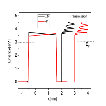
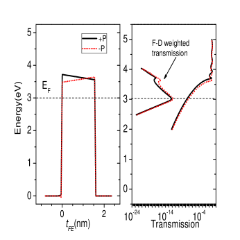
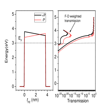
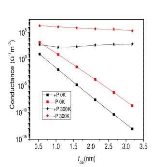
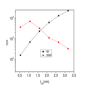
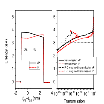
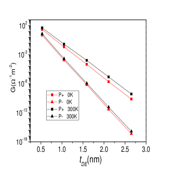
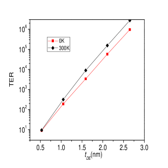
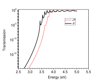
The first system to deal with is that of a BaTiO3 ferroelectric barrier on top of a SrRuO3 substrate which acts as contact layer, and on top of BaTiO3 is the Pt contact, which is considered as the left contact. Physical parameters are: nm, nm, , 2=8.45, FE=125, =3 eV, 1=2=3.6 eV, =16 C/cm2. The effective masses are: 5 m0 for SrRuO3, 2 m0 for BaTiO3, and m0 for Pt, where m0 is the free electron mass [30]. The Fermi energy is set to =3 eV. One should note that the electron effective masses are different in the three layers of the structure, hence the calculations need full numerical integration over transverse k wavevector in Eqs. (19) and (20). In Fig. 3 we show the potential profiles of a 2 nm thick BaTiO3 barrier for both directions of polarization. The transmission probability coefficients, also depicted in Fig. 3 right, exhibit resonances below and above the very top of the barriers. The resonances are associated with the peaks in the transmission spectra and if they are well resolved they obey Eq. (35). In Fig. 4 we plot the conductance of the system and in Fig.4 the TER ratio at 0K and 300K.
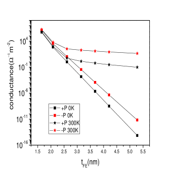
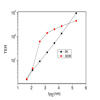
The calculation of the conductance at 300 K was performed with an applied bias of 0.0001 V which is low enough to satisfy the linear regime conditions. Both the conductance and TER ratio behave differently at 300K with respect to 0K. At 300K we observe two regimes depending on the ferroelectric thickness, one regime up to 2.5 nm and another one beyond that value. The difference between the two regimes is explained in Fig. 5. At 0K the channels open to electron flow are those up to Fermi energy represented by dashed line. These channels are those of direct tunneling such that the Simmons and Brinkman formulae are appropriate [17, 18, 19]. For the barrier of 1.6 nm thickness (Fig. 5) the transport occurs around Fermi energy even at room temperature (300K), hence that similar behavior of the conductance at 300K with respect to 0K, see Fig. 4. There is a small contribution to the transmitted current from the resonance states, but the contribution is orders of magnitude smaller. However, for thicker barriers, like the one shown in the Fig. 5, things may change. First, the direct tunneling current is much smaller since it has an exponential dependence on thickness. Second, the resonance levels are spaced much closer, hence their contribution increases considerably. Even if their occupancy, given by Fermi-Dirac function, might be small, it is offset by the large transmission probability. In Fig. 5 it can be easily seen that the contribution from resonance states is overwhelmingly larger than the contributions from states near the Fermi energy. Moreover, electrons with energies closer to the barrier top encounter a triangular barrier profile and so they may still reach a resonance state; this mechanism cannot be described within the semiclassical WKB theory of Fowler-Nordheim [21]. A similar behavior of the TER ratio at room temperature was also observed in experimental data [31]. It was found even a degradation of TER when increasing the ferroelectric thickness. However, performing their analysis based on Brinkman model at finite bias voltage, the authors attributed the TER degradation to the rather high levels of noise in the measurements.
III.1.2 Pt/SrTiO3 /BaTiO3 /SrRuO3 composite barrier FTJ
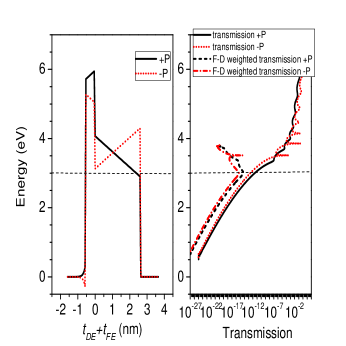
The second system we analyze is a composite TFJ, where a dielectric barrier (SrTiO is added beside the BaTiO3 ferroelectric barrier. The electrodes are Pt (left) and SrRuO3 (right). The role of the dielectric layer is to increase the asymmetry of the system, hence it is expected a higher TER ratio [32]. Physical parameters are slightly changed with respect the previous case [32, 33]: =0.045 nm, =0.08 nm, =2, =8.45, =90, =90,, =3 eV, ==3.6 eV, =0 eV, =20 C/cm2. The effective masses are: 5 m0 for SrRuO3, 2 m0 for BaTiO3 and SrTiO3, and m0 for Pt. In the following, BaTiO3 thickness is fixed to 2.4 nm and we have varied the SrTiO3 thickness from 0.5 nm to 3 nm. The results of calculations are presented in Fig. 6.
At 0K the conductance for both polarization directions shows an exponential dependence on dielectric thickness. At room temperature, on the other hand, it appears that this exponential dependence is no longer valid, as revealed by the TER ratio. In this case, a decrease of TER ratio takes place when the dielectric thickness increases (Fig. 6). The explanation of TER degradation is provided by the results presented in Fig. 7. One may observe that the electric charges are mainly transported through quantum states that a close or above the barrier top, the contribution of the states near the Fermi energy being negligible . The total barrier thickness is 3 nm at least, a value at which the resonance states start to play a significant role. As the barrier thickness is increased the contribution of the resonance states is enhanced. Nevertheless, those resonances located above the barrier (see the Fermi-Dirac wieghted curves in Fig. 7) become less sensitive to barrier profile and hence the decline of TER ratio with barrier thickness increase.
III.1.3 Metal/ CaO/BaTiO3/Metal composite FTJ
The third system studied herein is also a composite TFJ, with a CaO dielectric barrier added to the BaTiO3 ferroelectric barrier. The electrodes are of the same generic metal Me. In this case the asymmetry is ensured just by the presence of dielectric. We have set the the physical parameters to [32]: =0.1 nm, = =1, =90, =10,, =3 eV, =5.5 eV, =3.6 eV, =1.9 eV, =40 C/cm2. The effective masses are equal to m0 for all materials. We have also kept the thickness of BaTiO3 to 2.4 nm and we have varied the thickness of CaO from 0.5 nm to 3 nm. In comparison to the previous system, in this particular case the barrier is much higher on the dielectric side. The calculations of conductance and TER ratio are presented in Fig.8.
In contrast to Pt/SrTiO3/BaTiO3/SrRuO3, the conductance and the TER ratio of Me/CaO/BaTiO3/Me composite FTJ exhibit an exponential dependence on dielectric thickness at both 0K and 300K. Therefore, qualitatively at least, a 0K analysis remains valid also at room temperature. In Fig. 9 we show the data for a quantitative explanation of conductance and TER ratio behavior with temperature. One can see that resonance states have a minor contribution to the current; the vast majority of carriers are transported through states around Fermi energy, although there are many resonances below the top of the barrier. Due to the higher dielectric barrier, these resonance states are just weakly coupled to the contacts, hence they show low transmission coefficients and they have a modest contribution to conductance.
III.2 The tunneling wavefunctions. The wavefunctions of resonances
In the previous section it was discussed that the energy dependent transmission in FTJs has resonant features besides an exponential background. In this section we show that the wavefunctions also exhibit general features, some of which, e. g., those corresponding to resonances, are also observed in other nanostructures like quantum wells, multi-barrier structures, etc. Usually, as a scattering problem, the electron transport in FTJs has two solutions at a given energy: one solution for an incident electron wave coming from the left and the other for the electron wave coming from the right. In the following we will illustrate the wavefunctions at some representative energy values for two FTJs: Pt/BaTiO3/SrRuO3 and Pt/SrTiO3/BaTiO3/SrRuO3
III.2.1 The wavefunctions of Pt/BaTiO3/SrRuO3 FTJ
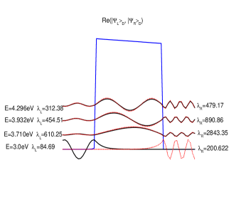
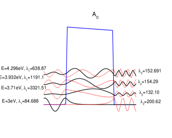
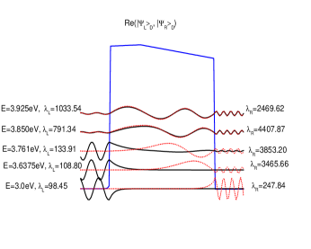
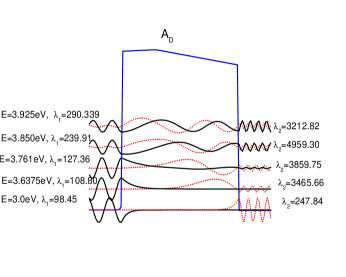
We illustrate the wave functions at Fermi energy (3 eV) and at some resonant energies like that can be taken from Fig. 10.
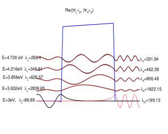
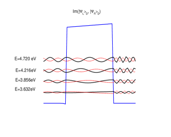
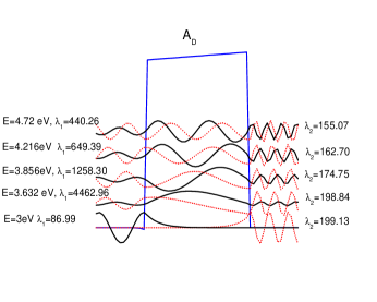
It is obvious that up to about 3.5 eV the transmission probability has an exponential dependence with respect to energy. In Fig. 11 we plotted the wavefunctions of a 1.6 nm thick BaTiO3 barrier at Fermi energy as well as the first few resonance energies for both directions of polarization. In order to compare those wavefunctions we plotted the “normalized” eigenvectors of , , and . In other words, for instance, are divided by and the eigenvectors of are divided by with , the corresponding eigenvalues. The device region is comprised of the barrier and several layers of contact regions, such that the region outside the device should exhibit a flat electrostatic potential. In practice this is achieved when a few nanometers of contacts are added to device region. At Fermi energy the wavefunctions are almost real and their overlap is almost zero. They decay exponentially in the barrier, hence the Simmons or Brinkman formula applies for states around Fermi energy.
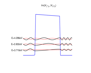
Since the barrier is thin the resonances are well separated. From Figs. 11, 11, and Figs. 11, 11 we see that the “normalized” is almost identical with the complex conjugation of “normalized”, however the values of provide the levels of electron density inside the device for the corresponding wavefunction. These states exhibit a confining character within the barrier, in contrast to the states shown at Fermi energy. These solutions belong to resonance and anti-resonance states in the complex wavevector plane [23, 25, 26]. Moreover, the real and the imaginary parts of can be found in the normalized eigenvectors of (Figs. 11 and 11). Finally, by analyzing Figs. 5 and 11, we notice that just the first resonance would participate to the electron transport at room temperature.
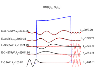
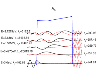
III.2.2 The wavefunctions of Pt/SrTiO3/BaTiO3/SrTiO3 composite FTJ
The plots of the wave functions for this composite FTJ are shown in Fig. 12. The transmission probability for polarizations is shown in Fig. 12 from which we can extract the resonances that play a role in the electron transport at room temperature. The physical parameters are those that have already been used in the calculations. The effective thickness of the barrier is larger than in simple FTJ presented in the previous subsection; hence the resonances are closely spaced. Still, at Fermi energy the wavefunctions decay exponentially in the barrier and are almost real, while their overlap is almost zero. The wavefunctions of the first four resonances in transmission have a much smaller imaginary part, which is not shown here. Like in the previous section, these wavefunctions manifest confining character in the barrier. Moreover, the dielectric induces a much smaller coupling to one of the two contacts, such that the first two resonances in transmission contain a significant background contribution as a decaying wavefunction in the barrier seen in the solution from the left (Fig. 12, positive polarization) and in the solution from the right (Fig. 12, negative polarization). Analyzing Figs 12 and 12 one can notice that the overlap between the solution from the left and that from the right is almost zero for the first two resonances in transmission. The next two resonances in transmission, however, can be distinguished from the background, the normalized eigenvectors of and , being quite similar, yet the corresponding wavefunctions and have quite different amplitudes. The difference in amplitudes starts to close in as we move to higher energies, since at sufficiently higher energy the asymmetry of the barrier will not play any major role in the electron transmission. As a final comment, all four resonances shown here participate to temperature activated transport (Fig. 7). However, the main contribution to temperature dependent transport is given by the first three resonances, even though the couplings to the contacts of the first two resonances are not so strong as the couplings of the third one which is further apart in energy.
IV Conclusions
In conclusion, the semi-empirical model of electrostatic and NEGF calculations can provide a detailed picture of electron transport in systems with FTJs. It treats on equal footing several transport mechanisms that are usually invoked when studying these devices like direct tunneling, thermionic emission, and Fowler-Nordheim tunneling. This feature of NEGF allows us to assess in detailed form the role of temperature in electron transport and how temperature affect TER ratio. We have found that for simple or composite BaTiO3 based FTJs the transport through temperature activated resonance (Gamow-Siegert) states may become dominant, affecting both the conductance and the TER ratio; thus, the more resonances are activated and the stronger their couplings to the contacts the more powerful is the effect of temperature. The effect of temperature is obvious in thicker FTJs, since the resonance states, especially those above the barrier, are closer to each other, hence more of them may participate in the transport. More insides into this phenomenology may be acquired by calculating and plotting the wavefunctions at any given energy. We show that this is possible for NEGF calculations of single-band transport. Thus the transport by direct tunneling is made through states whose wavefunctions have a decaying shape in the barrier. These states belong to the background generated by all resonance states. Furthermore, where the resonances are strong and well separated, the wavefunctions show confinement character in the barrier. In the intermediate regime, where the resonances are weak, the confining character of the resonance competes with the decaying character of the background. Lastly, we suggest that these thorough insights can be used in the optimization process of the FTJ design in various applications, particularly at high temperature.
Appendix A The BenDaniel and Duke Hamiltonian
The BenDaniel and Duke Hamiltonian
| (36) |
can be cast into 1D problem by rewriting it as
| (37) |
where is the effective mass in the left contact and
| (38) |
Equation (37) is discretized and its discrete form can be mapped into a tight-binding Hamiltonian. Thus the continuous variable is transformed in the discrete version n, where is the discretization step and is an integer running from - to . We define a localized orbital with n and as longitudinal and transverse positions. Moreover, we construct transverse Bloch orbitals as a sum over localized orbitals in the transverse plane
| (39) |
In this Bloch basis the Hamiltonian has the following expression
| (40) |
where
| (41) |
| (42) |
| (43) |
| (44) |
The tight-binding version (40) of BenDaniel and Duke Hamiltonian has a tridiagonal form. The left contact is defined for running from - to 0, the device is defined for running from 1 to , and the right contact from +1 to . The left and the right contacts are homogeneous systems; hence we define the tight-binding parameters as follows. The diagonal term of the left (right) contact is defined as (, while the off-diagonal terms as (.
Acknowledgements.
The authors acknowledge financial support from UEFISCDI Grant No. PN-III-P4-ID-PCE-2020-1985 and from the Romanian Core Program Contract No.14 N/2019 Ministry of Research, Innovation, and Digitalization.References
- Garcia and Bibes [2014] A. Garcia and M. Bibes, Nat. Commun. 5, 4289 (2014).
- .Guo et al. [2020] R. .Guo, W. Lin, X. Yan, T. Venkatesan, and J. Chen, Appl. Phys. Rev. 7, 011304 (2020).
- Zhuravlev et al. [2005] M. Y. Zhuravlev, R. F. Sabrianov, S. S. Jaswal, and E. Y. Tsymbal, Phys. Rev. Lett. 94, 246802 (2005).
- et al. [2005] H. K. , N. A. Pertsev, J. R. Contreras, and R. Waser, Phys. Rev. B 72, 125341 (2005).
- Zenkevich et al. [2013] A. Zenkevich, M. Minnekaev, Y. Matveyev, Y. Lebedinskii, K. Bulakh, A. Chouprik, A. Baturin, K. Maksimova, S. Thiess, and W. Drube, Appl. Phys. Lett. 102, 062907 (2013).
- Pantel et al. [2012] A. Pantel, H. Lu, S. Goetze, P. Werner, D. J. Kim, A. Gruverman, D. Hesse, and M. Alexe, Appl. Phys. Lett. 100, 232902 (2012).
- Hambe et al. [2010] M. Hambe, A. Petraru, N. A. Pertsev, P. M. V. Nagarajan, and H. Kohlstedt, Adv. Funct. Mater. 20, 2436 (2010).
- Mueller et al. [2012a] S. Mueller, J. Mueller, A. Singh, S. Riedel, J. Sundqvist, W. Schroeder, and T. Mikolajick, Adv. Funct. Mater. 22, 2412 (2012a).
- Mueller et al. [2012b] J. Mueller, T. S. Boscke, U. Schroder, S. Mueller, D. Brauhaus, U. Bottger, L. Frey, and T. Mikolajick, Nano Lett. 12, 4318 (2012b).
- abd D. Wu [2020] Z. W. abd D. Wu, Adv. Mater. 32, 1904123 (2020).
- Junquera and Gosez [2008] J. Junquera and P. Gosez, J. Comput. Theor. Nanosci. 5, 2071 (2008).
- Velev et al. [2016] J. P. Velev, J. D. Burton, M. Y. Zhuravlev, and E. Y. Tsymbal, npj Comput. Mater. 2, 16009 (2016).
- Bragato et al. [2018] M. Bragato, S. Achilli, F. Cargnoni, D. Ceresoli, R. Martinazzo, R. Soave, and M. I. Trioni, Materials 11, 2030 (2018).
- Chang et al. [2017] S. C. Chang, A. Naeemi, D. E. Nikonov, and A. Gruverman, Phys. Rev. Applied 7, 024005 (2017).
- Datta [2007] S. Datta, Quantum Transport: Atom to Transistor, 2nd ed. (Cambridge University Press, Cambridge, UK, 2007).
- Pantel and Alexe [2010] D. Pantel and M. Alexe, Phys. Rev. B 82, 134105 (2010).
- Simmons [1963] J. G. Simmons, J. Appl. Phys. 34, 1793 (1963).
- Gruverman et al. [2009] A. Gruverman, D. Wu, H. Lu, Y. Wang, H. W. Jang, C. M. Folkman, M. Y. Zhuravlev, D. Felker, M. Rzchowski, C. B. Eom, and E. Y. Tsymbal, Nano Lett. 9, 3539 (2009).
- Brinkman et al. [1970] W. F. Brinkman, R. C. Dynes, and J. M. Rowell, J. Appl. Phys. 41, 1915 (1970).
- Sze [2007] S. M. Sze, Physics of Semiconductor Devices, 3rd ed. (Wiley-Interscience, Hoboken, NJ, 2007).
- Fowler and Nordheim [1928] R. H. Fowler and L. Nordheim, Proc. R. Soc. Lond. A 119, 173 (1928).
- Lake et al. [1997] R. Lake, G. Klimeck, R. C. Bowen, and D. Jovanovic, J. Appl. Phys. 81, 7845 (1997).
- Garcia-Calderon [2010] G. Garcia-Calderon, Adv. Quantum Chem. 60, 407 (2010).
- Garcia-Calderon et al. [1993] G. Garcia-Calderon, R. Romo, and A. Rubio, Phys. Rev. B 47, 9572 (1993).
- Tolstikhin et al. [1997] O. I. Tolstikhin, V. N. Ostrovsky, and H. Nakamura, Phys. Rev. Lett. 79, 2026 (1997).
- Hatano and Ordonez [2011] N. Hatano and G. Ordonez, Int. J. Theor. Phys. 50, 1105 (2011).
- Chen et al. [1989] A. B. Chen, Y. M. Lai-Hsu, and W. Chen, Phys. Rev. B 39, 923 (1989).
- Paulsson and Brandbyge [2007] M. Paulsson and M. Brandbyge, Phys. Rev. B 76, 115117 (2007).
- Klimeck et al. [1995] G. Klimeck, R. Lake, R. C. Bowen, W. R. Frensley, and T. S. Moise, Appl. Phys. Lett. 67, 2539 (1995).
- He et al. [2019] J. He, Z. Ma, W. Geng, and X. Chou, Mater. Res. Express 6, 116305 (2019).
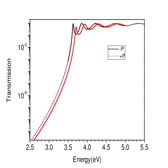
- Wang et al. [2016] L. Wang, M. R. Cho, Y. J. Shin, J. R. Kim, R. Das, J. G. Yoon, J. G. Chung, and T. W. Noh, Nano Lett. 16, 3911 (2016).
- Zhuravlev et al. [2009] M. Y. Zhuravlev, Y. Wang, S. Maekawa, and E. Y. Tsymbal, Appl. Phys. Lett. 95, 052902 (2009).
- Ma et al. [2019] Z. J. Ma, L. Q. Li, K. Liang, T. J. Zhang, N. Valanoor, H. P. Wu, Y. Y. Wang, and X. Y. Liu, MRS Communications 9, 258 (2019).