Spatially-Resolved Bandgap and Dielectric Function in 2D Materials from Electron Energy Loss Spectroscopy
Abstract
The electronic properties of two-dimensional (2D) materials depend sensitively on the underlying atomic arrangement down to the monolayer level. Here we present a novel strategy for the determination of the bandgap and complex dielectric function in 2D materials achieving a spatial resolution down to a few nanometers. This approach is based on machine learning techniques developed in particle physics and makes possible the automated processing and interpretation of spectral images from electron energy loss spectroscopy (EELS). Individual spectra are classified as a function of the thickness with -means clustering and then used to train a deep-learning model of the zero-loss peak background. As a proof-of-concept we assess the bandgap and dielectric function of InSe flakes and polytypic WS2 nanoflowers, and correlate these electrical properties with the local thickness. Our flexible approach is generalizable to other nanostructured materials and to higher-dimensional spectroscopies, and is made available as a new release of the open-source EELSfitter framework.
keywords:
Scanning Transmission Electron Microscopy, Electron Energy Loss Spectroscopy, Neural Networks, Machine Learning, van der Waals materials, Bandgap, Dielectric Function.Kavli]Kavli Institute of Nanoscience, Delft University of Technology, 2628CJ Delft, The Netherlands \altaffiliationEqual contribution Nikhef]Nikhef Theory Group, Science Park 105, 1098 XG Amsterdam, The Netherlands \alsoaffiliation[VU]Physics and Astronomy, VU Amsterdam, 1081 HV Amsterdam, The Netherlands \altaffiliationEqual contribution Kavli]Kavli Institute of Nanoscience, Delft University of Technology, 2628CJ Delft, The Netherlands \altaffiliationEqual contribution Kavli]Kavli Institute of Nanoscience, Delft University of Technology, 2628CJ Delft, The Netherlands Kavli]Kavli Institute of Nanoscience, Delft University of Technology, 2628CJ Delft, The Netherlands NIST]Materials Science and Engineering Division, National Institute of Standards and Technology, Gaithersburg, MD, 20899 USA NIST]Materials Science and Engineering Division, National Institute of Standards and Technology, Gaithersburg, MD, 20899 USA Nikhef]Nikhef Theory Group, Science Park 105, 1098 XG Amsterdam, The Netherlands \alsoaffiliation[VU]Physics and Astronomy, VU Amsterdam, 1081 HV Amsterdam, The Netherlands Kavli]Kavli Institute of Nanoscience, Delft University of Technology, 2628CJ Delft, The Netherlands
![[Uncaptioned image]](/html/2202.12572/assets/plots/TOC.png)
Introduction
Accelerating ongoing investigations of two-dimensional (2D) materials, whose electronic properties depend on the underlying atomic arrangement down to the single monolayer level, demands novel approaches able to map this sensitive interplay with the highest possible resolution. In this context, Electron Energy Loss Spectroscopy (EELS) analyses in Scanning Transmission Electron Microscopy (STEM) provide access to a plethora of structural, chemical, and local electronic information 1, 2, 3, 4, 5, from thickness and composition to the bandgap and complex dielectric function. Crucially, EELS-STEM measurements can be acquired as spectral images (SI), whereby each pixel corresponds to a highly localised region of the specimen. The combination of the excellent spatial and energy resolution provided by state-of-the-art STEM-EELS analyses 6, 7, 8 makes possible deploying EELS-SI as a powerful and versatile tool to realise the spatially-resolved simultaneous characterisation of structural and electric properties in nanomaterials. Such approach is complementary to related techniques such as cathodoluminescence in STEM (STEM-CL), which however is restricted to radiative processes while STEM-EELS probes both radiative and non-radiative processes 9, 10, 11.
Fully exploiting this potential requires tackling two main challenges. First, each SI is composed by up to tens of thousands of individual spectra, which need to be jointly processed in a coherent manner. Second, each spectra is affected by a different Zero-Loss Peak (ZLP) background 12, which depends in particular with the local thickness 13, 5. A robust subtraction of this ZLP is instrumental to interpret the low-loss region, , in terms of phenomena 11 such as phonons, excitons, intra- and inter-band transitions, and to determine the local bandgap. Furthermore, one should avoid the pitfalls of traditional ZLP subtraction methods 14, 15, 16, 17, 18, 19, 20, 21, 22 such as the need to specify an ad hoc parametric functional dependence.
In this work we bypass these challenges by presenting a novel strategy for the spatially-resolved determination of the bandgap and complex dielectric function in nanostructured materials from EELS-SI. Our approach is based on machine learning (ML) techniques originally developed in particle physics 23, 24, 25 and achieves a spatial resolution down to a few nanometers. Individual EEL spectra are first classified as a function of the thickness with -means clustering and subsequently used to train a deep-learning model of the dominant ZLP background 26. The resultant ZLP-subtracted SI are amenable to theoretical processing, in particular in terms of Fourier transform deconvolution and Kramers-Kronig analyses, leading to a precise determination of relevant structural and electronic properties at the nanoscale.
As a proof-of-concept we apply our strategy to the determination of the bandgap and the complex dielectric function in two representative van der Waals materials, InSe flakes and polytypic WS2 nanoflowers 27. Both electronic properties are evaluated across the whole specimen and can be correlated among them, e.g. to assess the interplay between bandgap energy or the location of plasmonic resonances with the local thickness. Our approach is amenable to generalisation to other families of nanostructured materials, is suitable for application to higher-dimensional datasets such as momentum-resolved EELS, and is made available as a new release of the EELSfitter open-source framework 26.
Computational Details
Spectral images in EELS-STEM are constituted by a large number, up to , of individual spectra acquired across the analysed specimen. They combine the excellent spatial resolution, , achievable with STEM with the competitive energy resolution, , offered by monochromated EELS. From these EELS-SI it is possible to evaluate key quantities such as the local thickness, the bandgap energy and type, and the complex dielectric function, provided one first subtracts the ZLP background which dominates the low-loss region of the EEL spectra. The information provided by an EELS-SI can hence be represented by a three-dimensional data cube, Fig. 1(a),
| (1) |
where indicates the total recorded intensity for an electron energy loss corresponding to the position in the specimen. This intensity receives contributions from the inelastic scatterings off the electrons in the specimen, , and from the ZLP arising from elastic scatterings and instrumental broadening, . In order to reduce statistical fluctuations, it is convenient to combine the information from neighbouring spectra using the pooling procedure described in the Supporting Information Sect. S1.
Since the ZLP intensity depends strongly on the local thickness of the specimen, first of all we group individual spectra as a function of their thickness by means of unsupervised machine learning, specifically by means of the -means clustering algorithm presented in Supporting Information Sect. S1. The cluster assignments are determined from the minimisation of a cost function, , defined in thickness space,
| (2) |
with being a binary assignment variable, equal to 1 if belongs to cluster ( for ) and zero otherwise, and with the exponent satisfying . Here represents the integral of over the measured range of energy losses, which provides a suitable proxy for the local thickness, and is the -th cluster mean. The number of clusters is a user-defined parameter.
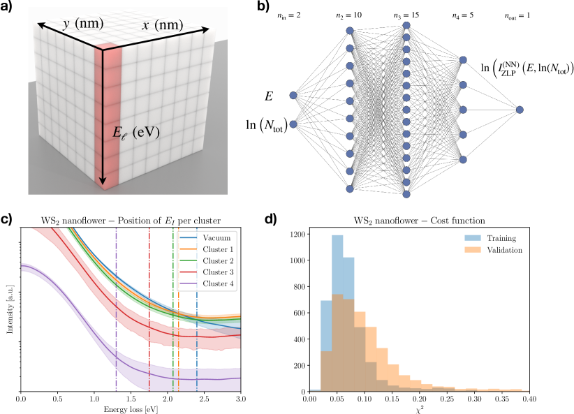
Subsequently to this clustering, we train a deep-learning model parametrising the specimen ZLP by extending the approach that we developed in 26. The adopted neural network architecture is displayed in Fig. 1(b), where the inputs are the energy loss and the integrated intensity . The model parameters are determined from the minimisation of the cost function
| (3) |
where within the -th thickness cluster a representative spectrum is randomly selected, and with being the variance within this cluster. The hyperparameters in Eq. (3) define the model training region for each cluster () where the ZLP dominates the total recorded intensity. They are automatically determined from the features of the first derivative , e.g. by demanding that only of the replicas have crossed , with . Typical values of are displayed in Fig. 1(c), where vacuum measurements are also included as reference. To avoid overlearning, the input data is separated into disjoint training and validation subsets, with the latter used to determine the optimal training length using look-back stopping 24. Fig. 1(d) displays the distribution of the training and validation cost functions, Eq. (3), evaluated over models. Both Figs. 1(c) and (d) correspond to the WS2 nanoflower specimen first presented in 26 and revisited here. Further details on the deep-learning model training are reported in Supporting Information Sect. S2.
This procedure is repeated for a large number of models , each based on a different random selection of cluster representatives, known in this context as “replicas”. One ends up with a Monte Carlo representation of the posterior probability density in the space of ZLP models, providing a faithful estimate of the associated uncertainties,
| (4) |
which makes possible a model-independent subtraction of the ZLP and hence disentangling the contribution from inelastic scatterings . Following a deconvolution procedure based in discrete Fourier transforms and reviewed in Supporting Information Sect. S3, these subtracted spectra allow us to extract the single-scattering distribution across the specimen and in turn the complex dielectric function from a Kramers-Kronig analysis. In contrast to existing methods, our approach provides an detailed estimate of the uncertainties associated to the ZLP subtraction, and hence quantifies the statistical significance of the determined properties by evaluating confidence level (CL) intervals from the posterior distributions in the space of models.
Results and discussion
As a proof-of-concept we apply our strategy to two different 2D material specimens. First, to horizontally-standing WS2 flakes belonging to flower-like nanostructures (nanoflowers) characterised by a mixed 2H/3R polytypism. This nanomaterial, member of the transition metal dichalcogenide (TMD) family, was already considered in the original study 27, 26 and hence provides a suitable benchmark to validate our new strategy. One important property of WS2 is that the indirect bandgap of its bulk form switches to direct at the monolayer level. Second, to InSe nanosheets prepared by exfoliation of a Sn-doped InSe crystal and deposited onto a holey carbon TEM grid. The electronic properties of InSe, such as the band gap value and type, are sensitive to both the layer stacking (, , or -phase) as well as to the magnitude and type of doping 28, 29, 30, 31. Supporting Information Sect. S5 provides further details on the structural characterisation of the InSe specimen.
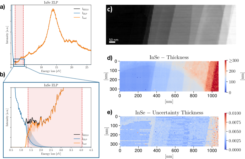
Fig. 2(a) shows a representative EEL spectrum from the InSe specimen, where the original data is compared with the deep-learning ZLP parametrisation and the subtracted inelastic contribution. The red dashed region indicates the onset of inelastic scatterings, from which the bandgap energy and type can be extracted from the procedure described in Supporting Information Sect. S4. We zoom in Fig. 2(b) in the low-loss region of the same spectrum, where the ZLP and inelastic components become of comparable size. The error bands denote the 68% CL intervals evaluated over Monte Carlo replicas.
By training the ZLP model on the whole InSe EELS-SI displayed in Fig. 2(c), see Fig. E.1(a,b) in the Supplementary Information for the corresponding STEM measurements, we end up with a faithful parameterisation of which can be used to disentangle the inelastic contributions across the whole specimen and carry out a spatially-resolved determination of relevant physical quantities. To illustrate these capabilities, Fig. 2(d,e) displays the maps associated to the median thickness and its corresponding uncertainties respectively for the same InSe specimen, where a resolution of 8 nm is achieved. One can distinguish the various terraces that compose the specimen, as well as the presence of the hole in the carbon film substrate as a thinner semi-circular region, see also the TEM analysis of Supporting Information Sect. S5 The specimen thickness is found to increase from around 20 nm to up to 300 nm as we move from left to right of the map, while that of the carbon substrate is measured to be around 30 nm consistent with the manufacturer specifications. Uncertainties on the thickness are below the 1% level, as expected since its calculation depends on the bulk (rather than the tails) of the ZLP.
In the same manner as for the thickness, the ZLP-subtracted SI contains the required information to carry out a specially-resolved determination of the bandgap. For this, we adopt the approach of 4 where the behaviour of in the onset region is modeled as
| (5) |
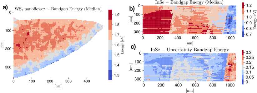
where both the bandgap energy and the exponent are extracted from a fit to the subtracted spectra. The value of the exponent is expected to be around for a semiconductor material characterised by a direct (indirect) bandgap. See Supporting Information Sect. S4 for more details of this procedure. Fig. 3(a) displays the bandgap map for the WS2 nanoflower specimen, where a mask has been applied to remove the vacuum and pure-substrate pixels. A value for the onset exponent is adopted, corresponding to the reported indirect bandgap. The uncertainties on are found to range between 15% and 25%. The map of Fig. 3(a) is consistent with the findings of Ref. 26 , which obtained a value of the bandgap of 2H/3R polytypic WS2 of eV with a exponent of from a single spectrum. These results also agree within uncertainties with first-principles calculations based on Density Functional Theory for the band structure of 2H/3R polytypic WS2 32. Furthermore, the correlation between the thickness and bandgap maps points to a possible dependence of the value of on the specimen thickness, though this trend is not statistically significant. Further details about the bandgap analysis of the WS2 nanoflowers are provided in Supporting Information Sect. S6.
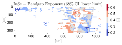
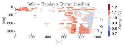
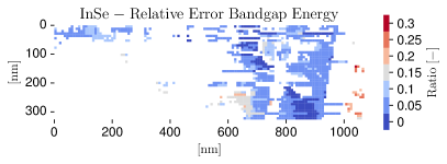
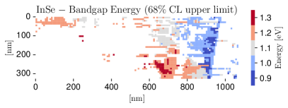
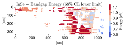
Moving to the InSe specimen, Figs. 3(b) and (c) display the corresponding maps for the median value of the bandgap energy and for its uncertainties, respectively. Photoluminescence (PL) measurements carried out on the same specimen, and described in the Supporting Information Sect. S5., indicate a direct bandgap with energy value around eV, hence we adopt for the onset exponent. The median values of are found to lie in the range between 0.9 eV and 1.3 eV, with uncertainties of 10% to 20% except for the thickest region where they are as large as 30%. This spatially-resolved determination of the bandgap of InSe is consistent with the spatially-averaged PL measurements as well as with previous reports in the literature 33. Interestingly, there appears to be a dependence of with the thickness, with thicker (thinner) regions in the right (left) parts of the specimen favoring lower (higher) values. This correlation, which remains robust once we account for the model uncertainties, is suggestive of the reported dependence of in InSe with the number of monolayers 34.
Within our approach it is also possible to determine simultaneously the exponent together with the bandgap energy . As already observed in Ref. 26 , this exponent is typically affected by large uncertainties. Nevertheless, it is found that in the case of the InSe specimen all pixels in the SI are consistent with and that the alternative scenario with is strongly disfavored. By retaining only those pixels where the determination of is achieved with a precision of better than 50%, one finds an average value of , confirming that indeed this material is a direct semiconductor and in agreement with the spatially-integrated PL results. In addition, the extracted values of are found to be stable irrespectively of whether the exponent is kept fixed or instead is also fitted. Supplementary Information Sect. S8 provides more details on the joint analysis.
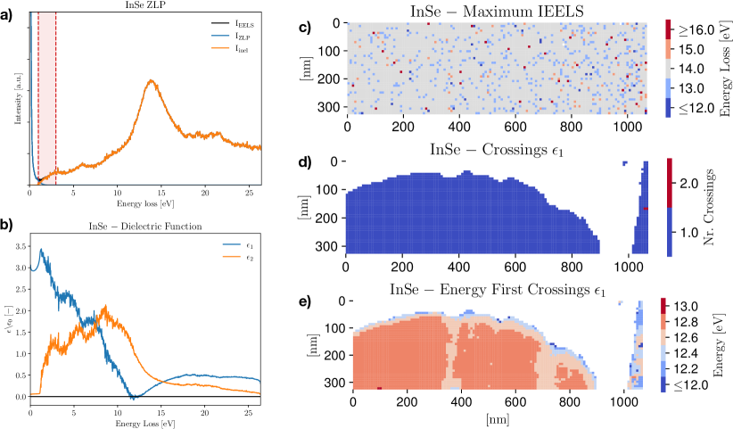
We evaluate now the properties of the complex dielectric function using the Kramers-Kronig analysis described in Supporting Information Sect. S3. In the following we focus on the InSe specimen, see Supporting Information Sect. S7 for corresponding results for the WS2 nanoflowers. The local dielectric function provides key information on the nature and location of relevant electronic properties of the specimen. To illustrate the adopted procedure, Fig. 4(a) displays another representative InSe spectrum from the same EELS-SI of Fig. 3(c). Noticeable features include a marked peak at eV, corresponding to the bulk plasmon of InSe, as well as a series of smaller peaks in the low-loss region. The real and imaginary parts of the complex dielectric function associated to the same location in the InSe specimen are shown in Fig. 4(b). The values of the energy loss for which the real component exhibits a crossing, , with a positive slope can be traced back to collective excitations such as a plasmonic resonances. Indeed, one observes how the real component exhibits a crossing in the vicinity of eV, consistent with the location of the bulk plasmon peak.
Furthermore, the local maxima of the imaginary component can be associated to interband transitions. From Fig. 4(b), one finds that exhibits local maxima in the low-loss region, immediately after the onset of inelastic scatterings, at energy losses around 3 eV, 6 eV, and 9 eV. The location of these maxima do match with the observed peaks in the low-loss region of Fig. 4(a), strengthening their interpretation of interband transitions between the valence and conduction bands, and consistent also with previous reports in the literature 35. The dielectric function in Fig. 4(b) provides also access to , the static dielectric constant and hence the refractive index of bulk InSe. Our results are in agreement with previous reports 36 once the thickness of our specimen is taken into account.
As for the thickness and the bandgap, one can also map the variation of relevant features in the dielectric function across the specimen. Extending the analysis of Figs. 4(a,b), Fig. 4(c) shows the value of the energy loss associated to the maximum of the inelastic scattering intensity , while Figs. 4(d,e) display the numbers of crossings of and the corresponding value of the energy loss respectively. In Figs. 4(d,e), the SI has been masked to remove pixels with carbon substrate underneath, the reason being that its contribution contaminates the recorded spectra and hence prevents from robustly extracting associated to InSe. It is found that the specimen exhibits a single crossing whose energy ranges between 12.5 eV and 13 eV, close to the maximum of and hence consistent with the location of the InSe bulk plasmonic resonance. Uncertainties on are below the 1% level, since the calculation of depends mildly on the onset region where model errors are the largest. Dielectric function maps such as Fig. 4(e) represent a sensitive method to chart the local electronic properties of a nanostructured material, complementing approaches such as fitting multi-Gaussian models to EELS spectra to identify resonances and transitions. In particular, maps for the local maxima of and could be also be constructed to gauge their variation across the specimen.
Interestingly, as was also the case for the bandgap energy in Fig. 3(c), by comparing Fig. 4(e) with Fig. 2(d) there appears to be a moderate correlation between the crossing energy and the specimen thickness, whereby decreases as the specimen becomes thicker. While dedicated theoretical and modelling work would be required to ascertain the origin of this sensitivity on the thickness, our results illustrate how our framework makes possible a precise characterisation of the local electronic properties of materials at the nanoscale and their correlation with structural features.
Summary and outlook
In this work we have presented a novel framework for the automated processing and interpretation of spectral images in electron energy loss spectroscopy. By deploying machine learning algorithms originally developed in particle physics, we achieve the robust subtraction of the ZLP background and hence a mapping of the low-loss region in EEL spectra with precise spatial resolution. In turn, this makes possible realising a spatially-resolved ( nm) determination of the bandgap energy and complex dielectric function in layered materials, here represented by 2H/3R polytypic WS2 nanoflowers and by InSe flakes. We have also assessed how these electronic properties correlate with structural features, in particular with the local specimen thickness. Our results have been implemented in a new release of the Python open-source EELS analysis framework EELSfitter, available from GitHub111 \urlhttps://github.com/LHCfitNikhef/EELSfitter, together with a detailed online documentation222 Available from \urlhttps://lhcfitnikhef.github.io/EELSfitter/index.html. .
While here we have focused on the interpretation of EELS-SI for layered materials, our approach is fully general and can be extended both to higher-dimensional datasets, such as momentum-resolved EELS 37 acquired in the energy-filtered TEM mode, as well as to different classes of nanostructured materials, from topological insulators to complex oxides. One could also foresee extending the method to the interpretation of nanostructured materials stacked in heterostructures, and in particular to the removal of the substrate contributions, e.g. for specimens fabricated on top of a solid substrate. In addition, in this work we have restricted ourselves to a subset of the important features contained in EEL spectra, while our approach could be extended to the automated identification and characterisation across the entire specimen (e.g. in terms of peak position and width) of the full range of plasmonic, excitonic, or intra-band transitions to streamline their physical interpretation. Finally, another exciting application of our approach would be to assess the capabilities of novel nanomaterials as prospective light (e.g. sub-GeV) Dark Matter detectors 38 by means of their electron energy loss function 39, which could potentially extend the sensitivity of ongoing Dark Matter searches by orders of magnitude.
Supporting Information
-
•
Technical details about the processing and theoretical interpretation of EELS spectral images and the ZLP subtraction.
-
•
Additional information about the determination of the bandgap energy and type as well as of the dielectric function.
-
•
Details on the structural characterisation of the InSe specimen, including PL measurements.
Acknowledgments
We are grateful to Irina Komen for carrying out the photoluminiscence measurements.
Funding
A B. and S. C.-B. acknowledge financial support from the ERC through the Starting Grant “TESLA”, grant agreement no. 805021. L. M. acknowledges support from the Netherlands Organizational for Scientific Research (NWO) through the Nanofront program. The work of J. R. has been partially supported by NWO. The work of J. t. H. is funded by NWO via a ENW-KLEIN-2 project. S. K. and A. V. D. acknowledge support through the Materials Genome Initiative funding allocated to NIST.
Certain commercial equipment, instruments, or materials are identified in this paper in order to specify the experimental procedure adequately. Such identification is not intended to imply recommendation or endorsement by NIST, nor is it intended to imply that the materials or equipment identified are necessarily the best available for the purpose.
Declaration of competing interest
The authors declare that they have no known competing financial interests or personal relationships that could have appeared to influence the work reported in this paper.
Methods
STEM-EELS measurements.
The STEM-EELS measurements corresponding to the WS2 specimen were acquired with a JEOL 2100F microscope with a cold field-emission gun equipped with aberration corrector operated at 60 kV. A Gatan GIF Quantum ERS System (Model 966) was used for the EELS analyses. The spectrometer camera was a Rio (CMOS) Camera. The convergence and collection semi-angles were 30.0 mrad and 66.7 mrad respectively. EEL spectra were acquired with an entrance aperture diameter of 5 mm, energy dispersion of 0.025 eV/ch, and exposure time of 0.001s. For the STEM imaging and EELS analyses, a probe current of 18.1 pA and a camera length of 12 cm were used. EEL spectra size in pixels was a height of 94 pixels and a width of 128 pixels. The EELS data corresponding to the InSe specimen were collected in a ARM200F Mono-JEOL microscope equipped with a GIF continuum spectrometer and operated at 200 kV. The spectrometer camera was a Rio Camera Model 1809 (9 megapixels). For these measurements, a slit in the monochromator of 1.3 m was used. A Gatan GIF Quantum ERS System (Model 966) was used for the EELS analyses with convergence and collection semi-angles of 23.0 mrad and 21.3 mrad respectively. EEL spectra were acquired with an entrance aperture diameter of 5 mm, energy dispersion of 0.015 eV/ch, and pixel time of 1.5 s. EEL spectra size in pixels was a height of 40 pixels and a width of 131 pixels. For the STEM imaging and EELS analyses, a probe current of 11.2 pA and a camera length of 12 cm were used.
Photoluminiscence measurements.
The optical spectra are acquired using a home-built spectroscopy set-up. The sample is illuminated through an 0.85 NA Zeiss 100x objective. The excitation source is a continuous wave laser with a wavelength of 595 nm and a power of 1.6 mW/mm2 (Coherent OBIS LS 594-60). The excitation light is filtered out using colour filters (Semrock NF03-594E-25 and FF01-593/LP-25). The sample emission is collected in reflection through the same objective as in excitation, and projected onto a CCD camera (Princeton Instruments ProEM 1024BX3) and spectrometer (Princeton Instruments SP2358) via a 4f lens system.
Appendix A Pooling and clustering of EELS-SI
Let us consider a two-dimensional region of the analysed specimen with dimensions where EEL spectra are recorded for pixels. Then the information contained within an EELS-SI may be expressed as
| (6) |
where indicates the recorded total electron energy loss intensity for an energy loss for a location in the specimen (pixel) labelled by , and is the number of bins that compose each spectrum. The spatial resolution of the EELS-SI in the and directions is usually taken to be the same, implying that
| (7) |
For the specimens analysed in this work we have spectra corresponding to a spatial resolution of nm. On the one hand, a higher spatial resolution is important to allow the identification and characterisation of localised features within a nanomaterial, such as structural defects, phase boundaries, surfaces or edges. On the other hand, if the resolution becomes too small the individual spectra become noisy due to limited statistics. Hence, the optimal spatial resolution can be determined from a compromise between these two considerations.
In general it is not known what the optimal spatial resolution should be prior to the STEM-EELS inspection and analysis of a specimen. Therefore, it is convenient to record the spectral image with a high spatial resolution and then, if required, combine subsequently the information on neighbouring pixels by means of a procedure known as pooling or sliding-window averaging. The idea underlying pooling is that one carries out the following replacement for the entries of the EELS spectral image listed in Eq. (6):
| (8) |
where indicates the pooling range, is a weight factor, and the pooling normalisation is determined by the sum of the relevant weights,
| (9) |
By increasing the pooling range , one combines the local information from a higher number of spectra and thus reduces statistical fluctuations, at the price of some loss on the spatial resolution of the measurement. For instance, averages the information contained on a square centered on the pixel . Given that there is no unique choice for the pooling parameters, one has to verify that the interpretation of the information contained on the spectral images does not depend sensitively on their value. In this work, we consider uniform weights, , but other options such as Gaussian weights
| (10) |
with as variance are straightforward to implement in EELSfitter. The outcome of this procedure is a a modified spectral map with the same structure as Eq. (6) but now with pooled entries. In this work we typically use to tame statistical fluctuations on the recorded spectra.
As indicated by Eq. (6), the total EELS intensity recorded for each pixel of the SI receives contributions from both inelastic scatterings and from the ZLP, where the latter must be subtracted before one can carry out the theoretical interpretation of the low-loss region measurements. Given that the ZLP arises from elastic scatterings with the atoms of the specimen, and that the likelihood of these scatterings increases with the thickness, its contribution will depend sensitively with the local thickness of the specimen. Hence, before one trains the deep-learning model of the ZLP it is necessary to first group individual spectra as a function of their thickness. In this work this is achieved by means of unsupervised machine learning, specifically with the -means clustering algorithm. Since the actual calculation of the thickness has as prerequisite the ZLP determination, see Eq. (46), it is suitable to use instead the total integrated intensity as a proxy for the local thickness for the clustering procedure. That is, we cluster spectra as a function of
| (11) |
which coincides with the sum of the ZLP and inelastic scattering normalisation factors. Eq. (11) is inversely proportional to the local thickness and therefore represents a suitable replacement in the clustering algorithm. In practice, the integration in Eq. (11) is restricted to the measured region in energy loss.
The starting point of -means clustering is a dataset composed by points,
| (12) |
which we want to group into separate clusters , whose means are given by
| (13) |
The cluster means represent the main features of the -th cluster to which the data points will be assigned in the procedure. Clustering on the logarithm of rather than on its absolute value is found to be more efficient, given that depending on the specimen location the integrated intensity will vary by orders of magnitude.
In -means clustering, the determination of the cluster means and data point assignments follows from the minimisation of a cost function. This is defined in terms of a distance in specimen thickness space, given by
| (14) |
with being a binary assignment variable, equal to 1 if belongs to cluster ( for ) and zero otherwise, and with the exponent satisfying . Here we adopt , which reduces the weight of eventual outliers in the calculation of the cluster means, and we verify that results are stable if is used instead. Furthermore, since clustering is exclusive, one needs to impose the following sum rule
| (15) |
The minimisation of Eq. (14) results in a cluster assignment such that the internal variance is minimised and is carried out by means of a semi-analytical algorithm. This algorithm is iterated until a convergence criterion is achieved, e.g. when the change in the cost function between two iterations is below some threshold. Note that, as opposed to supervised learning, here is it not possible to overfit and eventually one is guaranteed to find the solution that leads to the absolute minimum of the cost function. The end result of the clustering process is that now we can label the information contained in the (pooled) spectral image (for ) as follows
| (16) |
This cluster assignment makes possible training the ZLP deep-learning model across the complete specimen recorded in the SI accounting for the (potentially large) variations in the local thickness.
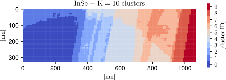
The number of clusters is a free parameter that needs to be fixed taking into consideration how rapidly the local thickness varies within a given specimen. We note that cannot be too high, else it will not be possible to sample a sufficiently large number of representative spectra from each cluster to construct the prior probability distributions, as required for the Monte Carlo method used in this work. We find that for the InSe and for the WS2 specimens are suitable choices. Fig. 5 displays the outcome of the -means clustering procedure applied to the InSe specimen, where each color represents one of the =10 thickness clusters. It can be compared with the corresponding thickness map in Fig. 2(d); the qualitative agreement further confirms that the total integrated intensity in each pixel represents a suitable proxy for the local specimen thickness.
Appendix B A deep-learning model for the zero-loss peak
Given that the zero-loss peak background cannot be evaluated from first principles, in this work we deploy supervised machine learning combined with Monte Carlo methods to construct a neural network parameterisation of the ZLP. Within this approach, one can faithfully model the ZLP dependence on both the electron energy loss and on the local specimen thickness. Our approach, first presented in 26, is here extended to model the thickness dependence and to the simultaneous interpretation of the spectra that constitute a typical EELS-SI. One key advantage is the robust estimate of the uncertainties associated to the ZLP modelling and subtraction procedures using the Monte Carlo replica method 40.
The neural network architecture adopted in this work is displayed in Fig. 2(b). It contains two input variables, namely the energy loss and the logarithm of the integrated intensity , the latter providing a proxy for the thickness . Both and are preprocessed and rescaled to lie between 0.1 and 0.9 before given as input to the network. Three hidden layers contain 10, 15, and 5 neurons respectively. The activation state of the output neuron in the last layer, , is then related to the intensity of the ZLP as
| (17) |
where an exponential function is chosen to facilitate the learning, given that the EELS intensities in the training dataset can vary by orders of magnitude. Sigmoid activation functions are adopted for all layers except for a ReLU in the final layer, to guarantee a positive-definite output of the network and hence of the predicted intensity.
The training of this neural network model for the ZLP is carried out as follows. Assume that the input SI has been classified into clusters following the procedure of App. A. The members of each cluster exhibit a similar value of the local thickness. Then one selects at random a representative spectrum from each cluster,
| (18) |
each one characterised by a different total integrated intensity evaluated from Eq. (11),
| (19) |
such that belongs to the -th cluster. To ensure that the neural network model accounts only for the energy loss dependence in the region where the ZLP dominates the recorded spectra, we remove from the training dataset those bins with with being a model hyperparameter 26 which varies in each thickness cluster. The cost function used to train the NN model is then
| (20) |
where the total number of energy loss bins that enter the calculation is the sum of bins in each individual spectrum, The denominator of Eq. (20) is given by , which represents the variance within the -th cluster for a given value of the energy loss . This variance is evaluated as the size of the 68% confidence level (CL) interval of the intensities associated to the -th cluster for a given value of .
For such a random choice of representative cluster spectra, Eq. (18), the parameters (weights and thresholds) of the neural network model are obtained from the minimisation of Eq. (20) until a suitable convergence criterion is achieved. Here this training is carried out using stochastic gradient descent (SGD) as implemented in the PyTorch library 41, specifically by means of the ADAM minimiser. The optimal training length is determined by means of the look-back cross-validation stopping. In this method, the training data is divided 80%/20% into training and validation subsets, with the best training point given by the absolute minimum of the validation cost function evaluated over a sufficiently large number of iterations.
In order to estimate and propagate uncertainties associated to the ZLP parametrisation and subtraction procedure, here we adopt a variant of the Monte Carlo replica method 26 benefiting from the high statistics (large number of pixels) provided by an EELS-SI. The starting point is selecting subsets of spectra such as the one in Eq. (18) containing one representative of each of the clusters considered. One denotes this subset of spectra as a Monte Carlo (MC) replica, and we denote the collection of replicas by
| (21) |
where now the superindices indicate a specific spectrum from the -th cluster that has been assigned to the -th replica. Given that these replicas are selected at random, they provide a representation of the underlying probability density in the space of EELS spectra, e.g. those spectra closer to the cluster mean will be represented more frequently in the replica distribution.
By training now a separate model to each of the replicas, one ends up with another Monte Carlo representation, now of the probability density in the space of ZLP parametrisations. This is done by replacing the cost function Eq. (20) by
| (22) |
and then performing the model training separately for each individual replica. Note that the denominator of the cost function Eq. (22) is independent of the replica. The resulting Monte Carlo distribution of ZLP models, indicated by
| (23) |
makes possible subtracting the ZLP from the measured EELS spectra following the matching procedure described in 26 and hence isolating the inelastic contribution in each pixel,
| (24) |
The variance of over the MC replica sample estimates the uncertainties associated to the ZLP subtraction procedure. By means of these MC samplings of the probability distributions associated to the ZLP and inelastic components of the recorded spectra, one can evaluate the relevant derived quantities with a faithful error estimate. Note that in our approach error propagation is realised without the need to resort to any approximation, e.g. linear error analysis.
One important benefit of Eq. (22) is that the machine learning model training can be carried out fully in parallel, rather than sequentially, for each replica. Hence our approach is most efficiently implemented when running on a computer cluster with a large number of CPU (or GPU) nodes, since this configuration maximally exploits the parallelization flexibility of the Monte Carlo replica method.
As mentioned above, the cluster-dependent hyperparameters ensure that the model is trained only in the energy loss data region where ZLP dominates total intensity. This is illustrated by the scheme of Fig. 3.3 in 26, which displays a toy simulation of the ZLP and inelastic scattering contributions adding up to the total recorded EELS intensity. The neural network model for the ZLP is then trained on the data corresponding to region I, while region II is obtained entirely from model predictions. To determine the values of , we evaluate the first derivative of the total recording intensity, , for each of the members of the -th cluster. When this derivative crosses zero, the contribution from will already be dominant. There are then two options. First, one sets , where and is the energy where the median of crosses zero (first local minimum) for cluster . Second, one sets to be the value where at most of the models have crossed , with . This choice implies that 90% of the models still exhibit a negative derivative. We have verified that compatible results are obtained with the two choices, indicating that results are reasonably stable with respect to the value of the hyperparameter .
The second model hyperparameter, denoted by in Fig. 3.3 in 26, indicates the region for which the ZLP can be considered as fully negligible. Hence in this region III we impose that by means of the Lagrange multiplier method. This condition fixes the model behaviour in the large energy loss limit, which otherwise would remain unconstrained. Since the ZLP is known to be a steeply-falling function, should not chosen not too far from to avoid an excessive interpolation region. In this work we use , though this choice can be adjusted by the user.
Finally, we mention that the model hyperparameters and could eventually be determined by means of an automated hyper-optimisation procedure as proposed in 42, hence further reducing the need for human-specific input in the whole procedure.
Appendix C Kramers-Kronig analysis of EEL spectra
Here we provide an overview of the theoretical formalism, based on 43, adopted to evaluate the single-scattering distribution, local thickness, bandgap energy and type and complex dielectric function from the measured EELS spectra. As indicated by Eq. (1) in the main manuscript, these spectra receive three contributions: the one from inelastic single scatterings off the electrons in the specimen, the one associated to multiple inelastic scatterings, and then the ZLP arising from elastic scatterings and instrumental broadening. Hence a generic EEL spectrum can be decomposed as
| (25) |
where is the energy loss experienced by the electrons upon traversing the specimen, is the ZLP intensity, and indicates the contribution associated to inelastic scatterings. The ZLP intensity can be further expressed as
| (26) |
where is known as the resolution or instrumental response function whose full width at half-maximum (FWHM) indicates the resolution of the instrument. The normalisation factor thus corresponds to the integrated intensity under the zero-loss peak. In the following, we assume that the ZLP contribution to Eq. (25) has already been disentangled from that associated to inelastic scatterings by means of the subtraction procedure described in App. B.
The single-scattering distribution.
If one denotes by the local thickness of the specimen and by the mean free path of the electrons, then assuming that inelastic scatterings are uncorrelated and that , one has that the integral over the -scatterings distribution is a Poisson distribution
| (27) |
with a normalisation constant. From the combination of Eqns. (25) and (27) it follows that
| (28) |
and hence one finds that the integral over the -scatterings distribution is such that
| (29) |
in terms of the normalisation of the full inelastic scattering distribution, the sample thickness and the mean free path . Note also that the ZLP normalisation factor is then given in terms of the inelastic one as
| (30) |
and hence one has the following relations between integrated inelastic scattering intensities
| (31) |
In order to evaluate the local thickness of the specimen and the corresponding dielectric function, it is necessary to deconvolute the measured spectra and extract from them the single-scattering distribution (SSD), . The SSD is related to the experimentally measured distribution, by the finite resolution of our measurement apparatus:
| (32) |
where in the following denotes the convolution operation. It can be shown, again treating individual scatterings as uncorrelated, that the experimentally measured and multiple scattering distributions can be expressed in terms of the SSD as
| (33) | |||||
| (34) |
and likewise for . Combining this information, one observes that the spectrum Eq. (25) can be expressed in terms of the resolution function , the ZLP normalisation , and the single-scattering distribution as follows
| (35) |
where is the Dirac delta function. If the ZLP normalisation factor and resolution function are known, then one can use Eq. (C) to extract the SSD from the measured spectra by means of a deconvolution procedure.
SSD deconvolution.
The structure of Eq. (C) indicates that transforming to Fourier space will lead to an algebraic equation which can then be solved for the SSD. Here we define the Fourier transform of a function as follows
| (36) |
whose inverse is given by
| (37) |
which has the useful property that convolutions such as Eq. (32) are transformed into products,
| (38) |
The Fourier transform of Eq. (C) leads to the Taylor expansion of the exponential and hence
| (39) |
which can be solved for the Fourier transform of the single scattering distribution
| (40) |
By taking the inverse Fourier transform, one obtains the sought-for expression for the single scattering distribution as a function of the electron energy loss
| (41) |
where the only required inputs are the experimentally measured EELS spectra, Eq. (25), with the corresponding ZLP.
Discrete Fourier transforms.
Eq. (41) can be evaluated numerically by approximating the continuous transform Eq. (36) by its discrete Fourier transform equivalent. The discrete Fourier transform of a discretised function defined at is given by:
| (42) |
with the corresponding inverse transformation being
| (43) |
If one approximates the continuous function by its discretised version and likewise by where one finds that
| (44) |
and likewise for the inverse transform
| (45) |
In practice, the EELS spectra considered are characterised by a fine spacing in and the discrete approximation for the Fourier transform produces results very close to the exact one.
Thickness calculation.
Once the SSD has been determined by means of the deconvolution procedure summarised by Eq. (41), it can be used as input in order to evaluate the local sample thickness from the experimentally measured spectra. Kramers-Kronig analysis provides the following relation between the thickness , the ZLP normalisation , and the single-scattering distribution,
| (46) |
where we have assumed that the effects of surface scatterings can be neglected. In Eq. (46), nm is Bohr’s radius, is a relativistic correction factor,
| (47) |
with being the incident electron energy, is the complex dielectric function, and is the characteristic angle defined by
| (48) |
with being the usual relativistic dilation factor, , and the collection semi-angle of the microscope.333Which should not be confused with the normalised velocity often used in relativity, . For either an insulator or a semiconductor material with refractive index , one has that
| (49) |
while for a metal or semi-metal. Hence, the determination of the dielectric function is not a pre-requisite to evaluate the specimen thickness, and for given microscope operation conditions we can express Eq. (46) as
| (50) |
with constant across the specimen. If the thickness of the specimen is already known at some location, then Eq. (50) can be used to calibrate and evaluate this thickness elsewhere. Furthermore, if the thickness of the material has already been determined by means of an independent experimental technique, then Eq. (46) can be inverted to determine the refractive index of an insulator or semi-conducting material using
| (51) |
The complex dielectric function.
The dielectric function of a material, also known as permittivity, is a measure of how easy or difficult it is to polarise a dielectric material such an insulator upon the application of an external electric field. In the case of oscillating electric fields such as those that constitute electromagnetic radiation, the dielectric response will have both a real and a complex part and will depend on the oscillation frequency ,
| (52) |
which can also be expressed in terms of the energy of the photons that constitute this electromagnetic radiation,
| (53) |
In the vacuum, the real and imaginary parts of the dielectric function reduce to and . Furthermore, the dielectric function is related to the susceptibility by
| (54) |
where is the so-called Coulomb matrix.
The single scattering distribution is related to the imaginary part of the complex dielectric function by means the following relation
| (55) |
in terms of the sample thickness , the ZLP normalisation , and the microscope operation parameters defined in Sect. C. We can invert this relation to obtain
| (56) |
Since the prefactor in Eq. (56) does not depend on the energy loss , we see that will be proportional to the single scattering distribution with a denominator that decreases with the energy (since ) and hence weights more higher energy losses.
Given that the dielectric response function is causal, the real part of the dielectric function can be obtained from the imaginary one by using a Kramers-Kronig relation of the form
| (57) |
where stands for Cauchy’s prescription to evaluate the principal part of the integral. A particularly important application of this relation is the case,
| (58) |
which is known as the Kramers-Kronig sum rule. Eq. (58) can be used to determine the overall normalisation of , since is known for most materials. For instance, as mentioned in Eq. (49), for an insulator or semiconductor material it is given in terms of its refractive index .
Once the imaginary part of the dielectric function has been determined from the single-scattering distribution, Eq. (56), then one can obtain the corresponding real part by means of the Kramers-Kronig relation, Eq. (57). Afterwards, the full complex dielectric function can be reconstructed by combining the calculation of the real and imaginary parts, since
| (59) |
implies that
| (60) |
and hence one can express the dielectric function in terms of experimentally accessible quantities,
| (61) |
Once the complex dielectric function of a material has been determined, it is possible to evaluate related quantities that also provide information about the opto-electronic properties of a material. One example of this would be the optical absorption coefficient, given by
| (62) |
which represents a measure of how far light of a given wavelength can penetrate into a material before it is fully extinguished via absorption processes. Furthermore, combining Eqns. (49) and (60) one has that for a semiconductor material, such as those considered in this work, the refractive index is given by the relation
| (63) |
which implies a positive, non-zero value of the real part of the complex dielectric function at .
The complex dielectric function provides direct information on the opto-electronic properties of a material, for example those associated to plasmonic resonances. Specifically, a collective plasmonic excitation should be indicated by the condition that the real part of the dielectric function crosses the axis, , with a positive slope. These plasmonic excitations typically are also translated by a well-defined peak in the energy loss spectra. Hence, verifying that a plasmonic transition indicated by corresponds to specific energy-loss features provides a valuable handle to pinpoint the nature of local electronic excitations present in the analysed specimen.
The role of surface scatterings.
The previous derivations assume that the specimen is thick enough such that the bulk of the measured energy loss distributions arises from volume inelastic scatterings, while edge- and surface-specific contributions can be neglected. However, for relatively thin samples with thickness below a few tens of nm, this approximation is not necessarily suitable. Assuming a locally flat specimen with two surfaces, in this case Eq. (25) must be generalised to
| (64) |
with representing the contribution from surface-specific inelastic scattering. This surface contribution can be evaluated in terms of the real and imaginary components of the complex dielectric function,
| (65) |
where the electron kinetic energy is .
The main challenge to evaluate the surface component from Eq. (65) is that it depends on the complex dielectric function , which in turn is a function of the single scattering distribution obtained from the deconvolution of obtained assuming that vanishes. For not too thin specimens, the best approach is then an iterative procedure, whereby one starts by assuming that , evaluates , and uses it to evaluate a first approximation to using Eq. (65). This approximation is then subtracted from Eq. (64) and hence provides a better estimate of the bulk contribution . One can then iterate the procedure until some convergence criterion is met. Whether or not this procedure converges will depend on the specimen under consideration, and specifically on the features of the EELS spectra at low energy losses, eV. For the specimens considered in this work, it is found that this iterative procedure to determine the surface contributions converges best provided that the local sample thickness satisfies nm.
Validation.
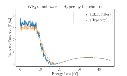
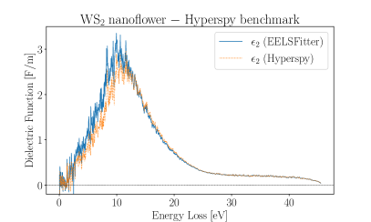
The calculations of the local specimen thickness, Eq. (46), and of the complex dielectric function, Eq. (61) presented in this work have been benchmarked with the corresponding implementation available within the HyperSpy framework 44. Provided one inputs the same inelastic spectra and ZLP parametrisation, agreement between the two calculations is obtained. This benchmark is illustrated in Fig. 6, which compares the EELSfitter-based results with those available from HyperSpy separately for the real and imaginary components of the dielectric function. Both calculations use for the same input ZLP and inelastic spectra, associated to a representative pixel of the WS2 nanoflower specimen. Residual differences can be attributed to implementation differences e.g. for the discrete Fourier transforms. This validation test further confirms the robustness of the calculations presented in this work.
Appendix D Band gap analysis of the EELS low-loss region
One important application of ZLP-subtracted EELS spectra is the determination of the bandgap energy and type (direct or indirect) in semiconductor materials. The reason is that the onset of the inelastic scattering intensity provides information on the value of the bandgap energy , while its shape for is determined by the underlying band structure. Different approaches have been put forward to evaluate from subtracted EEL spectra, such as by means of the inflection point of the rising intensity or a linear fit to the maximum positive slope 45, see also 46. Following 26, here we adopt the method of 4, 14, where the behaviour of in the region close to the onset of the inelastic scatterings is described by
| (66) |
and vanishes for . Here is a normalisation constant, while the exponent provides information on the type of bandgap: it is expected to be for a semiconductor material characterised by a direct (indirect) bandgap. While Eq. (66) requires as input the complete inelastic distribution, in practice the onset region is dominated by the single-scattering distribution, since multiple scatterings contribute only at higher energy losses.
The bandgap energy , the overall normalisation factor , and the bandgap exponent can be determined from a least-squares fit to the experimental data on the ZLP-subtracted spectra. This polynomial fit is carried out in the energy loss region around the bandgap energy, . A judicious choice of this interval is necessary to achieve stable results: a too wide energy range will bias the fit by probing regions where Eq. (66) is not necessarily valid, while a too narrow fit range might not contain sufficient information to stabilize the results and be dominated by statistical fluctuation.
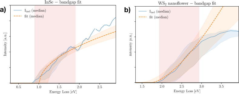
Fig. 7(a,b) displays representative examples of bandgap fits to the onset of the inelastic spectra in the InSe and WS2 specimens respectively. The red shaded areas indicate the fitting range, bracketed by and . The blue curve and band corresponds to the median and 68% CL intervals of the ZLP-subtracted intensity , and the outcome of the bandgap fits based on Eq. (66) is indicated by the green dashed curve (median) and band (68% CL intervals). Here the onset exponents have been kept fixed to for the InSe (WS2) specimen given the direct (indirect) nature of the underlying band-gaps. One observes how the fitted model describes well the behaviour of in the onset region for both specimens, further confirming the reliability of our strategy to determine the bandgap energy . As mentioned in 14, it is important to avoid taking a too large interval for , else the polynomial approximation ceases to be valid, as one can also see directly from these plots.
Appendix E Structural characterisation of the InSe specimen
Here we provide details on the structural characterisation of the -doped InSe specimens. Each specimen is composed by a InSe nanosheet exhibiting a range of thicknesses. The electronic properties of InSe, such as the band gap value and type, are sensitive to both the layer stacking (, , or -phase) as well as to the magnitude and type of doping 28, 29, 30, 31. In particular, -doped -phase InSe has been reported to exhibit a direct bandgap with value eV 33.
These InSe specimens have been grown by means of the Bridgman-Stockbarger method. Doping with Sn impurities is used to obtain -type InSe. InSe flakes are obtained from bulk material by the sonication procedure 47, whereby single InSe crystals are pulverized and added to IPA with a ratio of 2:1 (mg:ml). This combination is then sonicated in a sonic bath for 6 hours while keeping the temperature in the range between 25 ∘C and 35 ∘C. The ultra high frequencies lead to gas formation between the layers of the material, building up pressure until adjacent layers split apart. The flakes in the resulting suspension are then collected and dispersed on top of a TEM grid by pipetting.

Fig. 8(a) displays a low-magnification High-Angle Annular Dark Field (HAADF) STEM image of one of the specimens obtained from this procedure. The flake is lying on top of the holey carbon grid, and most of its volume is on top of the vacuum. Fig. 8(b) shows then a magnification of the region indicated with a red square in (a), while in turn the red rectangle in (b) marks the region where the corresponding EELS-SI, provided in Fig. 8(c), has been extracted. The spatial resolution in this EELS-SI is around 8 nm. Note that the (artificial) grey-scale convention adopted is different in Figs. 8(b) and (c). It can be observed that most of the flake turns out to be bulk, exhibiting thicknesses of several monolayers at least, with some thinner regions at the edges.
In order to identify the crystalline phase of the specimen under consideration, Fig. 9(a) displays a low-magnification HAADF-STEM image of a different InSe flake. This flake has been obtained from the same bulk material as that of Fig. 8(a) and hence shares its crystalline structure. Notice how this InSe flake is standing on top of a hole of the TEM grid. Fig. 9(b) then shows a high-resolution HAADF-STEM image corresponding to the red square in (a), and whose inset highlights the atomic arrangement in the region indicated with a red square. Fig. 9(c) provides the HAADF intensity line profile taken along the blue rectangle in (b), where the three colors correspond to the three-fold periodicity observed in the line profile. HAADF-STEM images are approximately proportional to , with being the atomic number. By comparing with the expectations based on possible atomic models, these images provide useful information to identify the underlying crystalline sequence. The line profile of Fig. 9(c) is consistent with the atomic model of -phase InSe shown in Fig. 9(d), both for top-view and for cross-view, and which uses the same choice of colors as in Fig. 9(c).
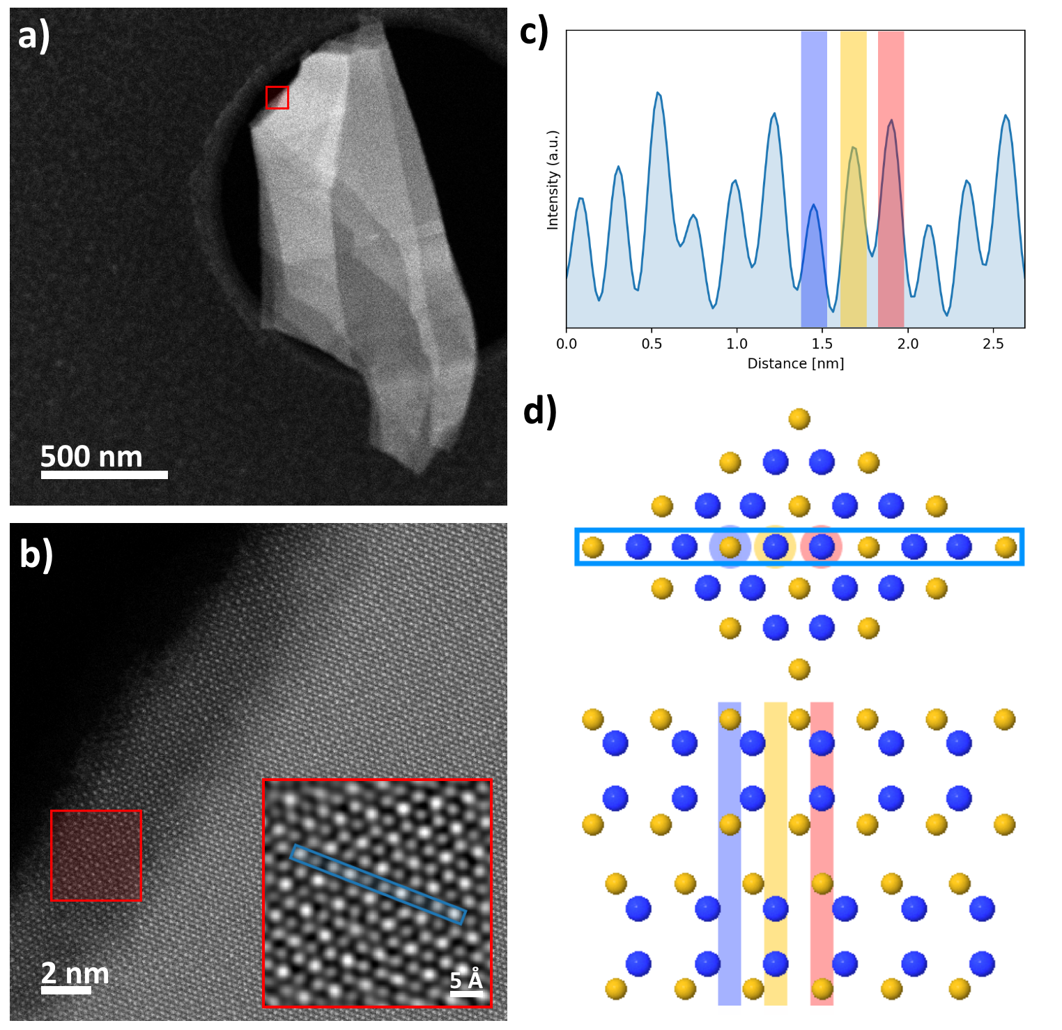
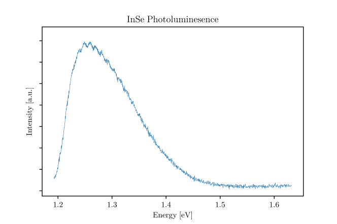
The structural analysis presented in Fig. 9 indicates that the -doped InSe specimens considered in this work exhibit a crystalline structure characterised by a pure -phase. In order to further elucidate the type of the bandgap exhibited by this material, photoluminescence (PL) measurements are carried out. The results, displayed in Fig. 10, exhibit a well-defined peak located around 1.26 eV. Hence, we conclude that this material is characterised by a direct bandgap with energy value eV, consistent with the findings of 33. Note that PL measurements are characterised by a limited spatial resolution as compared to the STEM-EELS results, and therefore this bandgap value corresponds to an average across the specimen. Hence, PL results are not sensitive to spatially-resolved features in the bandgap map such as those reported in Fig. 3(b) of the main manuscript.
Appendix F Bandgap analysis of 2H/3R WS2 nanoflowers
Here we apply our new approach to the bandgap analysis of same WS2 specimen considered in the original study 27, 26. This specimen consisted on a horizontally-standing WS2 flake belonging to flower-like nanostructures characterised by a mixed 2H/3R polytypism. While 26 restricted its bandgap analysis to a small subset of individual EELS spectra, here we extend it to the whole specimen and as a byproduct also we provide the local thickness map. The goal is to demonstrate how our updated analysis is consistent with the results presented in 26. The corresponding results for the dielectric function are presented in App. G.
Fig. 11 displays the outcome of the thickness map determination obtained using the EELS-SI from Fig. 5.1(a) of 26 as input. Fig. 11(a) shows the results of the -means clustering procedure for . The choice of clusters is found to be a good compromise between minimizing the variance within each cluster while ensuring a sufficiently large number of members, as required by the applicability the Monte Carlo replica method. The WS2 specimen itself turns out to be classified into three thickness clusters, surrounded by vacuum (dark blue) at the top and by the SiN substrate (red) in the bottom-right region of the map. Then Fig. 11(b) displays the corresponding thickness map evaluated by means of Eq. (46). Note that the image has been masked by retaining only the pixels associated to the WS2 specimen, to ease visualization. The qualitative agreement with the outcome of the -means clustering confirms the reliability of the total integrated intensity as a suitable proxy for the local specimen thickness when modelling the ZLP parametrisation.
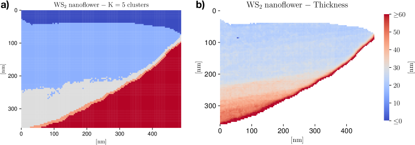
Fig. 12 then presents the corresponding bandgap analysis obtained from the same EELS-SI used to evaluate Fig. 11, where again the maps have been filtered such that only those pixels corresponding to the WS2 specimen are retained. First of all, Fig. 12(a) displays the spatially-resolved map displaying the median value of the bandgap energy evaluated across the WS2 specimen, where the spatial resolution achieved is around 10 nm. These bandgap energies have been obtained from the procedure described in App. D, specifically by fitting Eq. (66) to the onset of the inelastic spectra. A fixed value of the exponent , corresponding to the indirect bandgap reported for this material, is used to stabilize the model fit. Then Fig. 12(b) shows the associated relative uncertainty on the extracted bandgap energy. It is estimated as half the magnitude of the 68% CL interval (corresponding to one standard deviation for a Gaussian distribution) from the Monte Carlo replica sample for each pixel of the SI. One finds that the typical uncertainties range between 15% and 25%. Finally, Fig. 12(c) indicates the lower limit of the 68% CL interval for .
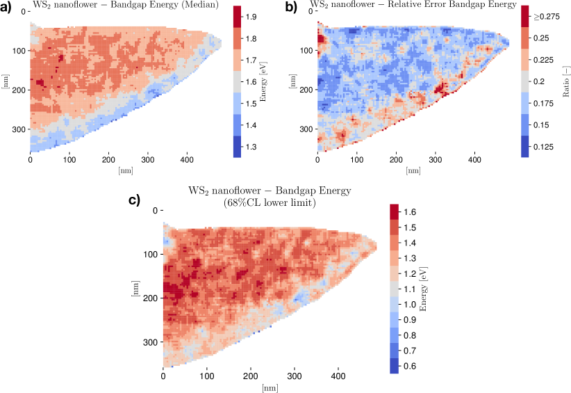
Ref. 26 reported a value of the bandgap of 2H/3R polytypic WS2 of eV with a exponent of extracted from single EELS spectrum. From the spatially-resolved bandgap maps of Fig. 12, one observes how our updated results are in agreement with those from the previous study within uncertainties. Furthermore, this spatially-resolved determination of is in agreement within uncertainties with first-principles calculations based on Density Functional Theory (DFT) of the band structure of 2H/3R polytypic WS2 32. These DFT calculations, which also account for spin-orbit coupling effects, find values of in the range between 1.40 eV and 1.48 eV depending on the settings of the calculation. The DFT predictions are hence consistent with the 68% CL interval for the for a wide region of the specimen, as indicated by Fig. 12(c).
Furthermore, inspection of the thickness and bandgap maps, Figs. 11(b) and 12(a) respectively, reveals an apparent dependence of the value of on the local specimen thickness. Specifically, the bandgap energies tend to increase in the thinner region of the specimen, with nm, and then to decrease as one moves towards the thicker regions with nm. While this dependence with the thickness is suggestive of the known property of WS2 that increases when going from bulk to monolayer form, uncertainties remain too large to be able to assign significance to this effect.
Appendix G Dielectric function in 2H/3R WS2 nanoflowers
App. F characterizes the local thickness and the bandgap energy of the 2H/3R WS2 nanoflower specimen from 27, 26 across the whole EELS-SI. We now present the corresponding results for the spatially-resolved determination of the real, , and imaginary, , parts of its complex dielectric function. Fig. 13 displays and corresponding to two representative spectra of this WS2 nanoflower specimen. In this analysis we account for the effects of the surface contributions and the error bands quantify the uncertainties associated to the ZLP subtraction procedure.
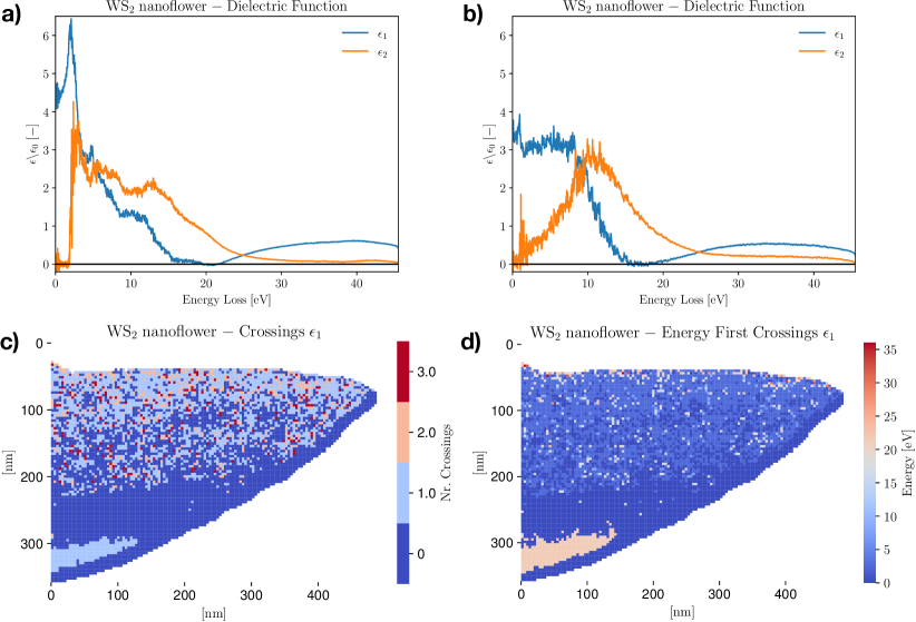
Of particular interest are the values of the energy loss for which the real component of the dielectric function exhibits a crossing, with a positive slope. These crossings can be interpreted as indicating a phase transition involving a collective electronic excitation, such as a plasmonic resonance. Here we define that a crossing takes place wherever at the 90% CL as estimated from the Monte Carlo representation. For the selected spectra displayed in Fig. 13(a,b), this condition is satisfied for eV and eV respectively. These values are consistent with the bulk and surface plasmonic resonances in 2H/3R polytypic WS2 identified in 27.
Fig. 13(c) displays the number of such crossings exhibited by the real part of the dielectric function across the whole WS2 nanoflower specimen. The vacuum and substrate regions have been masked such that only the spectra corresponding to the specimen are retained. One finds that the majority of the spectra are characterised by either one or zero crossings, while a minority showing two or even three crossings. By comparing with Fig. 11(b), one observes how it is in the thicker region of the specimen for which the condition is typically not satisfied, with the exception of the very bottom region which consistently displays one crossing.
Finally, Fig. 13(d) displays the energy associated to the left-most crossing in Fig. 13(c) for those pixels with crossings. For the upper region of the specimen (characterised by smaller thicknesses), the first crossing is found to be in the low-loss region, while in the bottom (thicker) region, one has a first crossing at eV consistent with the WS2 bulk plasmon peak. We note that one could also show the values of for the subsequent crossings, for those pixels exhibiting more than one crossing.
Appendix H Simultaneous determination of from EELS-SI
As discussed in the SI Sect. D, the ZLP-subtracted EELS spectra can be used to extract the value of the bandgap energy as well as its type (direct or indirect) in semiconductor material by fitting a functional form
| (67) |
to the onset region of the subtracted inelastic spectra, where corresponds to a direct (indirect) semiconductor. In the results presented in the main manuscript, in particular in Fig. 3, fits based on Eq. (67) were carried out by fixing the value of the exponent to for InSe specimen, motivated by the PL analysis, and for the WS2 nanoflower, justified by previous work 27, 26 as well as by independent first-principles DFT calculations 32. Here we present results of fits were both the bandgap energy and type are simultaneously determined from the ZLP-subtracted EELS spectra in the case of the InSe specimen.
Already in our original study 26, it was demonstrated that our method is suitable for the joint extraction of both the bandgap energy and the exponent simultaneously, but that in general the latter is affected by sizable uncertainties. For instance, for two of the EEL spectra considered there from the WS2 specimen, we found values and , consistent with the theoretical expectations for an indirect semiconductor. One option to reduce the model uncertainties on the exponent parameter would be to increase the pooling degree of the pixels in the SI, which would reduce the fluctuations in the low-loss region at the price of a degradation of the achieved spatial resolution. Here instead we show how we can obtain important information about the values of the exponent in a fully data-driven manner without compromising the spatial resolution. The strategy is to mask away the pixels where the joint determination of is too noisy, and hence retain only those pixels where the relative uncertainties on the two parameters is below a precision threshold.
Figs. 14 and 15 display the outcome of joint fits of where these two parameters are extracted simultaneously from the low-loss region of the subtracted EELS spectra for the InSe specimen. The upper panels display the median value and 68% CL relative uncertainty while the bottom panels show the values of the upper and lower ranges of the 68% CL interval, in the case of the exponent and of the bandgap energy respectively. Only those pixels where the relative uncertainty in the determination of both and is below the 50% level are retained, and the rest are masked away. One finds that for around of the pixels it is possible to achieve a reasonable precision in these joint fits of .
Inspection of Figs. 14 and 15 reveals that the EELS data strongly prefers a value of the exponent around , consistent with both the PL measurements and with the expectations of this material being a direct semiconductor, while an alternative scenario with is strongly disfavored. Furthermore, one can verify that for all other pixels in the SI, including the ones masked away, is contained within the 68% CL uncertainty range. If we average over all the SI pixels displayed in Fig. 14 we find , confirming that indeed the specimen is a direct semiconductor. In addition, by comparing with Fig. 3 (b,c) of the main manuscript, one finds that the extracted values of are stable irrespectively of whether the exponent is kept fixed or instead is fitted.
The analysis presented here demonstrates that our method is also suitable to provide spatially-resolved information about the value of the bandgap type, confirming the value of obtained from the spatially-averaged PL data. Further work will investigate how to improve the trade-off between spatial resolution and precision in the joint fits of from the subtracted EELS spectra.
References
- Geiger 1967 Geiger, J. Inelastic Electron Scattering in Thin Films at Oblique Incidence. Phys. Stat. Sol. 1967, 24, 457–460
- Schaffer et al. 2008 Schaffer, B.; Riegler, K.; Kothleitner, G.; Grogger, W.; Hofer, F. Monochromated, spatially resolved electron energy-loss spectroscopic measurements of gold nanoparticles in the plasmon range. Micron 2008, 40, 269–273
- Erni et al. 2005 Erni, R.; Browning, N. D.; Rong Dai, Z.; Bradley, J. P. Analysis of extraterrestrial particles using monochromated electron energy-loss spectroscopy. Micron 2005, 35, 369–379
- Rafferty and Brown 1998 Rafferty, B.; Brown, L. M. Direct and indirect transitions in the region of the band gap using electron-energy-loss spectroscopy. Phys. Rev. B 1998, 58, 10326
- Stöger-Pollach 2008 Stöger-Pollach, M. Optical properties and bandgaps from low loss EELS: Pitfalls and solutions. Nano Lett. 2008, 39, 1092–1110
- Terauchi et al. 2005 Terauchi, M.; M., T.; Tsuno, K.; Ishida, M. Development of a high energy resolution electron energy-loss spectroscopy microscope. J. Microsc. 2005, 194, 203–209
- Freitag et al. 2005 Freitag, B.; Kujawa, S.; Mul, P. M.; Ringnalda, J.; Tiemeijer, P. C. Breaking the spherical and chromatic aberration barrier in transmission electron microscopy. Ultramicroscopy 2005, 102, 209–214
- Haider et al. 1998 Haider, M.; Uhlemann, S.; Schwan, E.; Rose, H.; Kabius, B.; Urban, K. Electron microscopy image enhanced. Nature 1998, 392, 768–769
- Polman et al. 2019 Polman, A.; Kociak, M.; de Abajo, F. J. Electron-beam spectroscopy for nanophotonics. Nat. Mater. 2019, 18, 1158–1171
- de Abajo and Di Giulio 2021 de Abajo, F. J.; Di Giulio, V. Optical Excitations with Electron Beams: Challenges and Opportunities. ACS Photonics 2021, 8, 945–974
- de Abajo 2010 de Abajo, F. J. Optical excitations in electron microscopy. RevModPhys 2010, 82, 209–256
- Egerton 2009 Egerton, R. F. Electron energy-loss spectroscopy in the TEM. Rep. Prog. Phys 2009, 72, 1
- Park et al. 2008 Park, J.; Heo, S.; Others, Bandgap measurement of thin dielectric films using monochromated STEM-EELS. Ultramicroscopy 2008, 109, 1183–1188
- Rafferty et al. 2000 Rafferty, B.; Pennycook, S. J.; Brown, L. M. Zero loss peak deconvolution for bandgap EEL spectra. J. Electron Microsc. (Tokyo). 2000, 49, 517–524
- Egerton 1996 Egerton, R. F. Electron Energy-Loss Spectroscopy in the Electron Microscope; Plenum Press, 1996
- Dorneich et al. 1998 Dorneich, A. D.; French, R. H.; Müllejans, H.; Others, Quantitative analysis of valence electron energy-loss spectra of aluminium nitride. J. Microsc. 1998, 191, 286–296
- van Benthem et al. 2001 van Benthem, K.; Elsässer, C.; French, R. H. Bulk electronic structure of SrTiO3: Experiment and theory. J. Appl. Phys. 2001, 90
- Lazar et al. 2003 Lazar, S.; Botton, G. A.; Others, Materials science applications of HREELS in near edgestructure analysis an low-energy loss spectroscopy. Ultramicroscopy 2003, 96, 535–546
- Egerton and Malac 2002 Egerton, R.; Malac, M. Improved background-fitting algorithms for ionization edges in electron energy-loss spectra. Ultramicroscopy 2002, 92, 47–56
- Held et al. 2020 Held, J. T.; Yun, H.; Mkhoyan, K. A. Simultaneous multi-region background subtraction for core-level EEL spectra. Ultramicroscopy 2020, 210, 112919
- Granerød et al. 2018 Granerød, C. S.; Zhan, W.; Prytz, Ø. Automated approaches for band gap mapping in STEM-EELS. Ultramicroscopy 2018, 184, 39–45
- Fung et al. 2020 Fung, K. L. Y.; Fay, M. W.; Collins, S. M.; Kepaptsoglou, D. M.; Skowron, S. T.; Ramasse, Q. M.; Khlobystov, A. N. Accurate EELS background subtraction, an adaptable method in MATLAB. Ultramicroscopy 2020, 217, 113052
- Ball and Others 2009 Ball, R. D.; Others, A determination of parton distributions with faithful uncertainty estimation. Nucl. Phys. 2009, B809, 1–63
- Ball and Others 2015 Ball, R. D.; Others, Parton distributions for the LHC Run II. JHEP 2015, 04, 40
- Ball and Others 2017 Ball, R. D.; Others, Parton distributions from high-precision collider data. Eur. Phys. J. 2017, C77, 663
- Roest et al. 2021 Roest, L. I.; van Heijst, S. E.; Maduro, L.; Rojo, J.; Conesa-Boj, S. Charting the low-loss region in Electron Energy Loss Spectroscopy with machine learning. Ultramicroscopy 2021, 222, 113202
- van Heijst et al. 2021 van Heijst, S. E.; Mukai, M.; Okunishi, E.; Hashiguchi, H.; Roest, L. I.; Maduro, L.; Rojo, J.; Conesa-Boj, S. Illuminating the Electronic Properties of WS2 Polytypism with Electron Microscopy. Ann. Phys. 2021, 533, 2000499
- Gürbulak et al. 2014 Gürbulak, B.; cSata, M.; Dogan, S.; Duman, S.; Ashkhasi, A.; Keskenler, E. F. Structural characterizations and optical properties of InSe and InSe:Ag semiconductors grown by Bridgman/Stockbarger technique. Phys. E Low-dimensional Syst. Nanostructures 2014, 64, 106–111
- Julien and Balkanski 2003 Julien, C. M.; Balkanski, M. Lithium reactivity with III–VI layered compounds. Mater. Sci. Eng. B 2003, 100, 263–270
- Rigoult et al. 1980 Rigoult, J.; Rimsky, A.; Kuhn, A. Refinement of the 3R -indium monoselenide structure type. Acta Crystallogr. Sect. B 1980, 36, 916–918
- Lei et al. 2014 Lei, S.; Ge, L.; Najmaei, S.; George, A.; Kappera, R.; Lou, J.; Chhowalla, M.; Yamaguchi, H.; Gupta, G.; Vajtai, R. et al. Evolution of the Electronic Band Structure and Efficient Photo-Detection in Atomic Layers of InSe. ACS Nano 2014, 8, 1263–1272
- Maduro et al. 2022 Maduro, L.; van Heijst, S. E.; Conesa-Boj, S. First-Principles Calculation of Optoelectronic Properties in 2D Materials: The Polytypic WS2 Case. ACS Phys. Chem. Au 2022, in press
- Henck et al. 2019 Henck, H.; Pierucci, D.; Zribi, J.; Bisti, F.; Papalazarou, E.; Girard, J.-C.; Chaste, J.; Bertran, F. m. cc.; Le Fèvre, P.; Sirotti, F. et al. Evidence of direct electronic band gap in two-dimensional van der Waals indium selenide crystals. Phys. Rev. Mater. 2019, 3, 34004
- Hamer et al. 2019 Hamer, M. J.; Zultak, J.; Tyurnina, A. V.; Zólyomi, V.; Terry, D.; Barinov, A.; Garner, A.; Donoghue, J.; Rooney, A. P.; Kandyba, V. et al. Indirect to Direct Gap Crossover in Two-Dimensional InSe Revealed by Angle-Resolved Photoemission Spectroscopy. ACS Nano 2019, 13, 2136–2142
- Politano et al. 2017 Politano, A.; Campi, D.; Cattelan, M.; Ben Amara, I.; Jaziri, S.; Mazzotti, A.; Barinov, A.; Gürbulak, B.; Duman, S.; Agnoli, S. et al. Indium selenide: an insight into electronic band structure and surface excitations. Sci. Rep. 2017, 7, 3445
- Allakhverdiev et al. 1979 Allakhverdiev, K. R.; Babaev, S. S.; Salaev, E. Y.; Tagyev, M. M. Angular behaviour of the polar optical phonons in AIIIBVI layered semiconductors. Phys. status solidi 1979, 96, 177–182
- Senga et al. 2019 Senga, R.; Suenaga, K.; Barone, P.; Morishita, S.; Mauri, F.; Pichler, T. Position and momentum mapping of vibrations in graphene nanostructures. Nature 2019, 573, 247–250
- Knapen et al. 2017 Knapen, S.; Lin, T.; Zurek, K. M. Light Dark Matter: Models and Constraints. Phys. Rev. D 2017, 96, 115021
- Knapen et al. 2021 Knapen, S.; Kozaczuk, J.; Lin, T. Dark matter-electron scattering in dielectrics. Phys. Rev. D 2021, 104, 15031
- Del Debbio et al. 2007 Del Debbio, L.; Forte, S.; Latorre, J. I.; Piccione, A.; Rojo, J. Neural network determination of parton distributions: The nonsinglet case. JHEP 2007, 03, 39
- Paszke et al. 2019 Paszke, A.; Gross, S.; Massa, F.; Lerer, A.; Bradbury, J.; Chanan, G.; Killeen, T.; Lin, Z.; Gimelshein, N.; Antiga, L. et al. In Adv. Neural Inf. Process. Syst. 32; Wallach, H., Larochelle, H., Beygelzimer, A., d'Alché-Buc, F., Fox, E., Garnett, R., Eds.; Curran Associates, Inc., 2019; pp 8024–8035
- Ball et al. 2021 Ball, R. D.; Carrazza, S.; Cruz-Martinez, J.; Del Debbio, L.; Forte, S.; Giani, T.; Iranipour, S.; Kassabov, Z.; Latorre, J. I.; Nocera, E. R. et al. The path to proton structure at one-percent accuracy. arXiv preprint arXiv:2109.02653 2021,
- Egerton 2007 Egerton, R. F. Limits to the spatial, energy and momentum resolution of electron energy-loss spectroscopy. Ultramicroscopy 2007, 107, 575–586
- de la Peña et al. 2021 de la Peña, F.; Prestat, E.; Fauske, V. T.; Burdet, P.; Furnival, T.; Jokubauskas, P.; Nord, M.; Ostasevicius, T.; Lähnemann, J.; MacArthur, K. E. et al. hyperspy/hyperspy: Release v1.6.3. 2021; \urlhttps://doi.org/10.5281/zenodo.4923970
- Schamm and Zanchi 2003 Schamm, S.; Zanchi, G. Study of the dielectric properties near the band gap by VEELS:gap measurement in bulk materials. Ultramicroscopy 2003, 96, 559–564
- Dimitrievska et al. 2021 Dimitrievska, M.; Hage, F. S.; Escobar Steinvall, S.; Litvinchuk, A. P.; Stutz, E. Z.; Ramasse, Q. M.; i Morral, A. The Advantage of Nanowire Configuration in Band Structure Determination. Adv. Funct. Mater. 2021, 31, 2105426
- Petroni et al. 2018 Petroni, E.; Lago, E.; Bellani, S.; Boukhvalov, D. W.; Politano, A.; Gürbulak, B.; Duman, S.; Prato, M.; Gentiluomo, S.; Oropesa-Nuñez, R. et al. Liquid-Phase Exfoliated Indium–Selenide Flakes and Their Application in Hydrogen Evolution Reaction. Small 2018, 14, 1800749