Proximity spin-orbit and exchange coupling in ABA and ABC
trilayer graphene van der Waals heterostructures
Abstract
We investigate the proximity spin-orbit and exchange couplings in ABA and ABC trilayer graphene encapsulated within monolayers of semiconducting transition-metal dichalcogenides and the ferromagnetic semiconductor Cr2Ge2Te6. Employing first-principles calculations we obtain the electronic structures of the multilayer stacks and extract the relevant proximity-induced orbital and spin interaction parameters by fitting the low-energy bands to model Hamiltonians. We also demonstrate the tunability of the proximity effects by a transverse electric field. Using the model Hamiltonians we also study mixed spin-orbit/exchange coupling encapsulation, which allows to tailor the spin interactions very efficiently by the applied field. We also summarize the spin-orbit physics of bare ABA, ABC, and ABB trilayers, and provide, along with the first-principles results of the electronic band structures, density of states, spin splittings, and electric-field tunabilities of the bands, qualitative understanding of the observed behavior and realistic model parameters as a resource for model simulations of transport and correlation physics in trilayer graphene.
I Introduction
Two-dimensional (2D) van der Waals (vdW) materials are vital building blocks in the design of ultracompact electronic and spintronic devices Han et al. (2014); Fabian et al. (2007); Gong and Zhang (2019); Li et al. (2019); Cortie et al. (2019). In this context, proximity-induced phenomena Zutic et al. (2019); Sierra et al. (2021) were found to be of great importance, since 2D materials influence each others electronic and spin properties in vdW heterostructures. Recently, it has been demonstrated that superconductivity Li et al. (2020); Moriya et al. (2020); Trainer et al. (2020), magnetism Zollner et al. (2016, 2018, 2019a, 2020a); Zhang et al. (2015, 2018); Vila et al. (2021); Wang et al. (2015); Xu et al. (2018); Yang et al. (2013); Zhong et al. (2020); Averyanov et al. (2018); Ciorciaro et al. (2020), and spin-orbit coupling (SOC) Gmitra and Fabian (2015); Gmitra et al. (2016); Zollner and Fabian (2019, 2021a); Song et al. (2018); Zhang et al. (2014); Avsar et al. (2017, 2014); Alsharari et al. (2018); Frank et al. (2016), can be induced on demand in such weakly glued vdW multilayers. In addition, gating, twisting, stacking, and straining are efficient tunability knobs to tailor these spin interactions Zollner et al. (2019a); Song et al. (2018); David et al. (2019); Avsar et al. (2017); Ghiasi et al. (2019); Benitez et al. (2020); Luo et al. (2017); Safeer et al. (2019); Herling et al. (2020); Zollner and Fabian (2021b); Naimer et al. (2021), while the individual materials also preserve a great degree of autonomy.
In twisted vdW heterostructures Carr et al. (2017); Hennighausen and Kar (2021); Ribeiro-Palau et al. (2018); Carr et al. (2020) the interlayer interaction can be controlled by the twist angle. In this context, bilayer graphene (BLG) was the first model playground for gate- and twist-tunable correlated physics Cao et al. (2018a, b); Arora et al. (2020); Stepanov et al. (2020); Lu et al. (2019); Sharpe et al. (2019); Ribeiro-Palau et al. (2018), as well as for layer-dependent proximity-induced spin interactions Gmitra and Fabian (2017); Amann et al. (2021); Zollner et al. (2020b); Lin et al. (2022); Wang et al. (2019); Zollner et al. (2018); Island et al. (2019); Cardoso et al. (2018); Tiwari et al. (2021); Zollner and Fabian (2021c). At very small twist angles (), a sharp peak arises in the density of states (DOS) of twisted BLG, which is associated with flat bands Bistritzer and MacDonald (2011) in the dispersion. By doping the twisted BLG, it can become insulating, ferromagnetic Sharpe et al. (2019), or superconducting Cao et al. (2018a, b); Arora et al. (2020); Stepanov et al. (2020); Lu et al. (2019); Nimbalkar and Kim (2020); Saito et al. (2020). As a logical next step, also twisted BLG-BLG structures were considered Shen et al. (2020); Liu et al. (2020); Cao et al. (2020); Burg et al. (2019), where the flat bands are additionally tunable by a gate field.
In addition, recent experiments Lin et al. (2022) could demonstrate that the proximity-induced Rashba and valley Zeeman SOC in twisted-BLG/WSe2 heterostructures, induces orbital magnetism without the need for a rotational alignment to a hexagonal boron-nitride substrate Sharpe et al. (2019); Serlin et al. (2020). Moreover, the transition-metal dichalcogenide (TMDC) WSe2 can help to stabilize superconductivity in twisted BLG Arora et al. (2020), emphasizing the role of the dielectric environment. For the interpretation of such experimental results, it is also important to have qualitative and quantitative knowledge about the proximity effects in TMDC/BLG heterostructures Zollner and Fabian (2021c).
Unlike mono- and bilayer graphene, trilayer graphene (TLG) has not yet been systematically investigated for spin proximity effects. The spin-orbit physics of pristine TLG in ABA and ABC stackings was investigated by ab-initio calculations Konschuh (2011) and tight-binding modeling Kormányos and Burkard (2013), revealing many subtleties of the low-energy bands stemming from the presence of -orbitals which give rise to spin-orbit splittings on the order of 10 eV. Depending on the stacking order of the three layers, either ABA or ABC, very different electronic structures can be realized with distinct features in electronic and spin transport Jhang et al. (2011); Ghosh and Misra (2012) and gate tunable SOC Chen et al. (2012). TLG is also important from the topological perspective, since the ABC structure potentially hosts quantum spin Hall and quantum valley Hall states Rehman and Abid (2017), while there is evidence for a giant topological magnetic moment in ABA TLG Ge et al. (2021). Also interesting is the energetics of the different stackings, see, for example, Ref. Guerrero-Avilés et al. (2021)
More recently, TLG has emerged as a novel platform for correlated electrons Zhu et al. (2020); Park et al. (2021); Chen et al. (2019a, 2020, b); Zhou et al. (2021a); Polshyn et al. (2020), as there is one more independent layer, leading to a wider range of magic angles. As a consequence, the tunability of the electronic and superconducting properties are superior to the ones in BLG, as recently demonstrated Park et al. (2021); Phong et al. (2021); Zhou et al. (2021b); Qin and MacDonald (2021); Cao et al. (2021) and theoretically explained Chou et al. (2021). Remarkably, a zero-field superconducting diode, signalling an interplay of spin-orbit physics and time-reversal symmetry broken phase, has been demonstrated in twisted-TLG/WSe2 heterostructures Siriviboon et al. (2021); Lin et al. (2021); Scammell et al. (2021). For the interpretation and quantitative theoretical understanding of such experiments it is important to have a deeper microscopic knowledge of the spin proximity effects in TLG. Providing such a resource is the goal of our manuscript.
In particular, we investigate, by performing first-principles calculations, the electronic structures of ABA and ABC TLG encapsulated within strong SOC semiconductors MoSe2 and WSe2 and ferromagnetic monolayers Cr2Ge2Te6 (CGT). We provide the essential band structure information, low-energy band dispersions, spin splittings of the low-energy bands, spin textures, and the behavior of the Dirac bands in the presence of a transverse electric field. To provide reference for the encapsulated systems, we summarize the essential low energy physics of bare ABA and ABC TLG, also including ABB TLG for completeness. While pristine graphene exhibits intrinsic SOC of 10–20 eV, encapsulated TLG displays spin splittings of some meV, strongly tunable by the electric field.
In terms of modeling, we focus on the proximity-induced spin-orbit and exchange couplings, and demonstrate that in order to reproduce the density functional theory (DFT) data, it is sufficient to modify only the spin interactions of the outer layers of encapsulated TLG. The effective low-energy Hamiltonians, which are fitted to the TLG dispersions to obtain reasonable parameter sets, nicely reproduce the first-principles data. Moreover, we show that the model reproduces the data also in the presence of a transverse electric field, whereby modifying only a few effective couplings is sufficient for a quantitative comparison.
Employing the model, with fitted proximity spin-orbit and exchange couplings separately, we then provide predictions for ex-so-tic heterostructures Zollner et al. (2020b); exs which comprise both a strong SOC monolayer and a ferromagnetic monolayer, encapsulating ABA and ABC TLG. The interplay between spin-orbit and exchange coupling is imprinted onto the corresponding low-energy band structures and most markedly pronounced by the different band dispersions at and . We also show that the band dispersions respond sensitively to the applied electric field, which can serve as a knob to change the spin polarization of the low-energy states in ABC TLG.
In all the studied cases we provide both qualitative understanding, based on the atomic arrangement and hybridization across the layers, and quantitative modeling with realistic parameters fitted to the DFT results, which should be useful for model simulations of TLG.
The paper is organized as follows: In section II, we first discuss the electronic properties of bare TLG with ABA, ABC, and ABB stackings, under the influence of SOC and an external electric field, to have reference results for the encapsulated structures. In section III, we present the encapsulated TLG geometries, address the structural setup, and summarize the calculation details for obtaining the electronic structures. In section IV, we introduce the model Hamiltonians that capture the low energy physics of encapsulated TLG (including orbital, SOC, and exchange terms), which are used to fit the DFT-calculated dispersions. In section V, we then show and discuss the DFT-calculated electronic structures, along with the model Hamiltonian fits, of TMDC and CGT encapsulated TLG. In section VI, we turn to the electric field tunability of the relevant low energy bands of TMDC encapsulated TLG. In section VII, we discuss the interplay of spin interactions in CGT/TLG/TMDC heterostructures, on the model level, based on our results for TMDC and CGT encapsulated TLG. Finally, in section VIII we conclude the manuscript.
II Bare trilayer graphene
Recent investigations on twisted-graphene/BLG heterostructures, that contain all three high-symmetry TLG stacking types (ABA, ABC, and ABB), reveal highly interesting topological properties Polshyn et al. (2020); Rademaker et al. (2020); Park et al. (2020); Ma et al. (2021). For example, in Ref. Polshyn et al. (2020) the electrical control of magnetism, which arises due to strong correlations by twisting graphene on top of BLG, has been demonstrated.
To have reference results for evaluating the proximity effects in encapsulated graphene trilayers, we briefly review the essential electronic properties of bare ABA, ABC, and ABB stackings, focusing on the energy dispersions of the lowest energy bands and the spin-orbit splittings. The electronic band structures of the bare trilayers were obtained by performing first-principles calculations employing a full potential linearized augmented plane wave (FLAPW) code based on density functional theory (DFT), as implemented in WIEN2k Blaha et al. (2001). This code was already used to calculate SOC in monolayer and bilayer graphene, Gmitra et al. (2009); Konschuh et al. (2010, 2012), yielding results consistent with recent experimental findings Sichau et al. (2019); Banszerus et al. (2020).
In our implementation, exchange-correlation effects are treated with the generalized-gradient approximation (GGA) Perdew et al. (1996), including the DFT-D3 vdW dispersion correction Grimme et al. (2010). We used a very dense -point grid of to accurately determine the Fermi level. The Muffin-tin radius of carbon atoms is and the plane wave cutoff parameter . For all TLG stackings, we use the lattice parameter of bare graphene Å, with fixed interlayer distances of Å. In order to avoid interactions between periodic images of our slab geometries, we add a vacuum of about Å in the direction. An earlier account of WIEN2k TLG calculations can be found in Ref. Konschuh (2011), while multi-orbital tight-binding modeling of ABC TLG in the presence of SOC was performed in Ref. Kormányos and Burkard (2013).
II.1 ABA

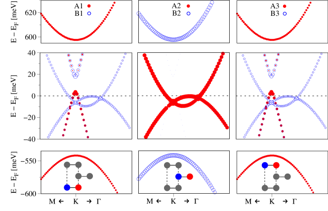
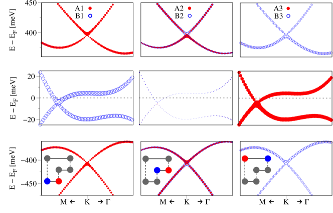
In Fig. 1 we show the lattice structure, the calculated energy dispersion, and a schematic energy level diagram for ABA TLG. Due to -mirror symmetry, four nonequivalent atoms are present in the geometry, see Fig. 1(a). The low-energy band structure, see Fig. 1(b), shows graphene-like Dirac states, as well as BLG-like parabolic bands, consistent with literature Partoens and Peeters (2006); Latil and Henrard (2006); Koshino and McCann (2009a); Aoki and Amawashi (2007). The Dirac bands are exclusively formed by orbitals of the atoms in the outermost graphene layers. In contrast, the parabolic bands are formed by atoms B1, A2, and B3, which form non-dimer interlayer pairs.
Without SOC, the bands remain spin-degenerate, see the scheme in Fig. 1(c). Including SOC, the degeneracy is lifted due to the absence of space-inversion symmetry and the low-energy bands are split by about 20 eV (corresponding to the intrinsic SOC of pristine graphene monolayers Gmitra et al. (2009)). The high-energy states — not shown in Fig. 1(b) but included in the energy level diagram in Fig. 1(c) — which are formed by atoms A1, B2, and A3, are about 500 meV away from the Dirac point at the Fermi level. The reason is that these atoms are coupled by direct interlayer hopping, pushing the corresponding bands away from the Fermi level, similar to bare BLG Konschuh et al. (2012). The spin-orbit splittings of the high-energy bands are just a few eV. The diagram in Fig. 1(c) also indicates the effect of an applied transverse electric field which introduces a potential difference between the outermost layers. The field essentially reshuffles the energy levels, but mainly the band offsets of the Dirac and parabolic low-energy bands change, while the spin-orbit splittings remain nearly unchanged for the electric field as large as 0.2 V/nm. In appendix A, we show and discuss the evolution of the ABA TLG dispersion and DOS for electric fields up to 1 V/nm. We also provide model Hamiltonian fit results there, that nicely reproduce the dispersion.
II.2 ABC
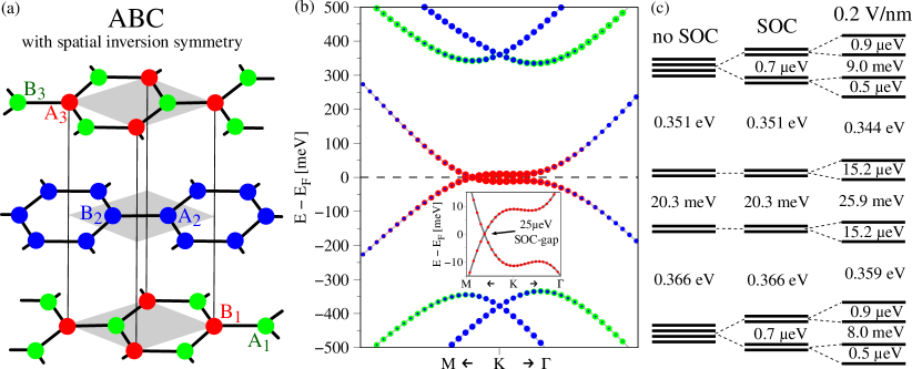
In Fig. 2 we show the lattice structure, the calculated energy dispersion, and an energy-level diagram for ABC TLG. This structure has spatial inversion symmetry and only three nonequivalent atoms are present in the geometry, see Fig. 2(a). From the band structure at the point, see Fig. 2(b), we find two flat low-energy bands which are formed by the outer-layer atoms B1 and A3, although A2 and B2 become prominent at larger momenta away from . The four high-energy bands, which are split off from the Fermi level by more than 0.35 eV, are built by sublattices A1, A2, B2, and B3. The presented dispersion is consistent with earlier reports Latil and Henrard (2006); Koshino and McCann (2009b); Aoki and Amawashi (2007); Zhang et al. (2010); Lu et al. (2006).
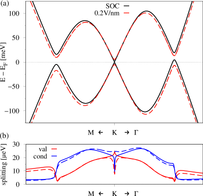
At the point, the low-energy bands are twofold spin degenerate, while the high-energy bands are even fourfold degenerate, in the absence of SOC, see Fig. 2(c). Due to spatial inversion symmetry, all bands remain spin degenerate, even when SOC is turned on. However, a tiny (about 0.7 eV) spin-orbit gap opens at the high-energy levels and removes the fourfold degeneracy. Zooming into the Fermi level, we find a cone-like touching feature of the low-energy bands along the high-symmetry line, see Fig. 2(b). When SOC is included, the Dirac cones are split by 25 eV, which corresponds to the spin-orbit gap, caused almost solely by orbitals of a pristine graphene monolayer Gmitra et al. (2009).
When a perpendicular electric field is applied across the ABC TLG, the inversion symmetry, along with the spin degeneracy of the bands, gets lifted, see Fig. 2(c). The field introduces a potential difference between the outermost layers, leading to further gap openings in the spectrum. By increasing the field amplitude, the low-energy spin splittings at the point first increase, then saturate at about eV, and finally decrease again Konschuh (2011). For a field of 0.2 V/nm, the splittings of the low-energy bands at the point are about eV, see Fig. 2(c). Near the Dirac cone vertex, the band splittings are eV, again corresponding to the intrinsic SOC of monolayer graphene Gmitra et al. (2009). Such intrinsic splittings, that get exposed by an applied electric field and that do not depend on the field above some crossover value, are also present in BLG Konschuh et al. (2012) and lead to a marked spin relaxation anisotropy as already experimentally detected Leutenantsmeyer et al. (2018).
II.3 ABB
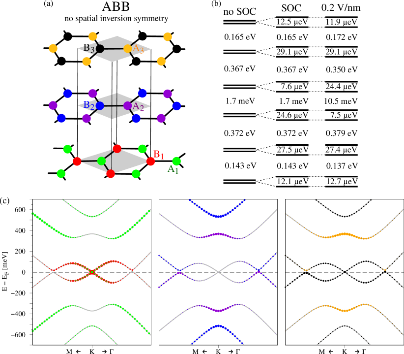
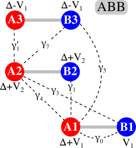
In Fig. 3 we show the lattice structure, the calculated dispersion, and an energy level diagram for ABB TLG. Due to the absence of spatial inversion and -mirror symmetry, all sublattice atoms are different, see Fig. 3(a). The band structure, see Fig. 3(c), features parabolic high-energy bands at around 600 meV at the point, predominantly formed by B2 atoms. The reason is that B2 is interlayer-coupled to both surrounding layers, splitting these states off to high energies. The low-energy bands near the point are almost exclusively formed by B1, with a small contribution from A1 and B3. The reason is that B1 does not couple directly to the other layers, so the corresponding band remains close to the Dirac point. The intermediate bands are formed by A2 and A3 near the point, because they are only connected by one interlayer coupling. The energy level diagram, see Fig. 3(b), shows that the bands remain spin-degenerate without SOC. Including SOC lifts the degeneracy, because spatial inversion symmetry is absent. The low-energy valence (conduction) band is split by about 25 eV (8 eV). A transverse electric field further opens the gap at the point, while swapping the spin-orbit splittings—and the orbital composition of the bands themselves—of the low-energy valence and conduction bands (see also Fig. 18 in appendix B). The high-energy bands remain nearly the same, except that band offsets are tunable by the field. In Appendix B we show the evolution of the ABB TLG dispersion and DOS for electric fields up to 1 V/nm. We also provide model Hamiltonian fit results there, that nicely reproduce the dispersion.
For the presented TLG dispersions, we have fixed all the interlayer distances to Å. In Appendix C we compare the dispersions and DOS for ABA, ABC, and ABB TLG with relaxed interlayer distances. Especially the ABB dispersion and DOS are markedly modified, since the interlayer distances become highly asymmetric.
II.4 Electric Field Effects

An important factor for correlation physics in TLG is the flatness of the dispersion, associated with van Hove singularities (VHS) in the DOS. Recently, superconductivity in ABC TLG was demonstrated Zhou et al. (2021b), which is certainly strongly related with the electric field tunability of these VHS. Below we describe the electric tunability of ABC TLG, while in appendices A and B we show and discuss the electric field behavior of ABA and ABB TLG dispersions and their corresponding DOS.
In Fig. 4 we show the evolution of the dispersion and DOS for ABC TLG for electric fields up to 1 V/nm. The field opens a band gap at the Fermi level, since the low-energy bands are formed by atoms B1 and A3 (see Fig. 2) of the outermost graphene layers, now located in different potentials. Increasing the field up to 1 V/nm opens a sizable gap of about 90 meV in the spectrum. Also in the high-energy bands, gaps are introduced by the field. However, because they are split-off in energy from the Fermi level, they are not so important for transport experiments. Viewing the corresponding DOS, we find VHS associated with the low-energy bands. As the electric field separates these bands in energy, they further flatten and the VHS become strongly pronounced.
Given the similarity of the electric field behavior of the low energy bands of BLG Konschuh et al. (2012) and ABC TLG, one can expect, for example, similar tunability of the valley g-factor as demonstrated for BLG Moulsdale et al. (2020); Lee et al. (2020). Moreover, one can also expect a spin-orbit valve operation in ABC TLG, as experimentally and theoretically demonstrated in BLG/TMDC heterostructures Gmitra and Fabian (2017); Island et al. (2019).
III Encapsulated Trilayer Graphene
III.1 Geometry Setup
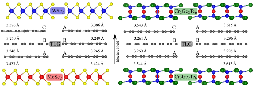
In the following we focus on TLG in ABA and ABC stacking, which are of most current interest. For both stacking types, we consider supercells of TLG to be encapsulated by monolayer supercells of bottom MoSe2 and top WSe2. In the case of TMDC encapsulation, we use the lattice constant of pristine TLG () and the MoSe2 and WSe2 lattice constants are barely strained (below 0.3% Schutte et al. (1987); James and Lavik (1963)) to . Moreover, in the case of TMDC encapsulation, the twist angles between all layers is . Here, we do not investigate different twist angles. Note that the electronic structures of TMDCs are very sensitive to strain Zollner et al. (2019b), especially in terms of band gap. In contrast, the Dirac states of graphene are quite robust against biaxial strain Si et al. (2016); Choi et al. (2010). Moreover, upon twisting, proximity SOC in graphene/TMDC heterostructures can be strongly modified, which has been investigated in Refs. David et al. (2019); Li and Koshino (2019); Naimer et al. (2021). Especially in Ref. Naimer et al. (2021), DFT calculations have shown that straining graphene, while leaving the TMDC unstrained, determines the position of the Dirac states within the TMDC band gap. This band offset can be tuned by gating, thereby influencing proximity SOC. We believe that these findings would also apply for our heterostructures of TMDC encapsulated TLG.
In addition, we consider supercells of TLG to be encapsulated within supercells of ferromagnetic CGT. In the case of CGT encapsulation, we also keep the lattice constant of pristine TLG but stretch the CGT lattice constant by roughly 4% from Carteaux et al. (1995) to , for better comparability of the encapsulation cases. Note that, similar to the TMDCs, CGT also shows a strain-tunable band gap Li and Yang (2014); Chen et al. (2015); Liu et al. (2021). Again, the twist angle is crucial for proximity exchange in graphene/CGT heterostructures Zollner and Fabian (2021b). In our geometries, the relative twist angle between top (bottom) CGT and the top (bottom) graphene layer is . In Ref. Zollner and Fabian (2021b), it has been explicitly shown by DFT calculations, that mainly twisting influences proximity exchange, while straining determines the position of the graphene Dirac states within the CGT band gap. This band offset is again tunable by gating, thereby influencing proximity exchange. Also these findings should be applicable for our TLG structures.
Initial atomic structures are set up with the atomic simulation environment (ASE) Bahn and Jacobsen (2002) and visualized with VESTA software Momma and Izumi (2011), see Fig. 5. Our choice of the encapsulating monolayers is based on the fact that TMDCs and CGT are semiconductors, providing strong spin-orbit and exchange couplings to graphene, correspondingly Gmitra et al. (2016); Gmitra and Fabian (2015); Zollner et al. (2018, 2020b); Zollner and Fabian (2021c). Another important factor for our choice is the lattice matching, such that the different materials can be combined in commensurate supercells for periodic DFT calculations, without straining them beyond reasonable limits.
III.2 Computational Details
The electronic structure calculations and structural relaxations of the TLG-based vdW heterostructures are performed by DFT Hohenberg and Kohn (1964) with Quantum ESPRESSO Giannozzi et al. (2009). Self-consistent calculations are performed with the -point sampling of to get converged results for the proximity-induced exchange and SOC. We use an energy cutoff for the charge density of Ry, and the kinetic energy cutoff for wavefunctions is Ry for the scalar relativistic pseudopotentials with the projector augmented wave method Kresse and Joubert (1999) with the Perdew-Burke-Ernzerhof exchange correlation functional Perdew et al. (1996). In the case of CGT encapsulation, we perform open shell calculations that provide the spin polarized ground state and proximity exchange coupling. In addition, a Hubbard parameter of eV is used for Cr -orbitals, similar to recent calculations Gong et al. (2017); Zollner et al. (2018); Zollner and Fabian (2021c). In the case of TMDC encapsulation, we use the relativistic versions of the pseudopotentials, to capture (proximity) SOC effects.
For the relaxation of the heterostructures, we add DFT-D2 vdW corrections Grimme (2006); Barone et al. (2009) and use quasi-newton algorithm based on trust radius procedure. Dipole corrections Bengtsson (1999) are also included to get correct band offsets and internal electric fields. In order to simulate quasi-2D systems, we add a vacuum of Å, to avoid interactions between periodic images in our slab geometries. To determine the interlayer distances, the atoms of TLG and the TMDCs are allowed to relax only in their positions (vertical to the layers), and the atoms of CGT are allowed to move in all directions, until all components of all forces are reduced below [Ry/], where is the Bohr radius. The obtained interlayer distances are summarized in Fig. 5 and are similar to previous reports Gmitra and Fabian (2017); Zollner et al. (2018, 2020b). Since we have assumed perfectly aligned individual layers, the full heterostructures still have symmetry after relaxation.
IV Model Hamiltonians
Here we present the Hamiltonians that we employ to model the low-energy bands of the (encapsulated) ABA and ABC TLG. The basis states are , , , , , , providing 12 eigenvalues , for both spin species of each C atom. In this basis the Hamiltonian comprises several terms Konschuh (2011); Zhang et al. (2010); Koshino and McCann (2009b); Kormányos and Burkard (2013); Koshino (2010)
| (1) |
The orbital terms for ABA and ABC TLG consist of intra- and interlayer hoppings
| (2) | ||||
| (3) |
The spin-orbit coupling and exchange terms are the same for both stackings in the above basis:
| (4) |
We use the linearized version of the nearest-neighbor structural function , with the graphene lattice constant and the Cartesian wave vector components and are measured from for the valley indices . The Pauli spin matrices are , with , and . Here, , , describe intra- and interlayer hoppings in TLG, see Fig. 6 for an overview. The coupling is the nearest neighbor intralayer hopping amplitude between A and B sublattice within each graphene layer. The parameter describes the direct interlayer hopping between A and B sublattice of adjacent graphene layers. Similarly, parameters , , and are also vertical interlayer hoppings, but between the outermost layers in TLG. In addition, the hoppings and are interlayer couplings, but not vertical. They connect next nearest neighbor atoms of adjacent graphene layers. Vertical hoppings in TLG couple only two atoms, hence they appear without structural function in the Hamiltonian, while the other hoppings couple an atom to three corresponding partner atoms, hence they appear linear in momentum.
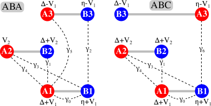

In general, due to the proximity effect the three layers experience different energy potentials, which we describe by assigning to the middle layer and to the outer layers. In addition, asymmetries and arise due to the vertical hoppings ( and in ABC TLG; , , and in ABA TLG). The combination of parameters , , , and can then describe the on-site energies of the individual sublattices of the different layers within TLG. The parameters () describe the intrinsic or proximity-induced spin-orbit or exchange couplings of the corresponding layer and sublattice atom (). The parameters represent the Rashba terms of the bottom and top layers . The middle layer, formed by atoms and , is far away from the proximitizing TMDC and CGT encapsulation layers. Therefore, we can neglect the corresponding proximity SOC and exchange parameters, as we will see from the band structure fits. Actually, in the ABC TLG orbital Hamiltonian, the additional factors of 2 in front of and in the diagonal entries arise due to SOC Konschuh (2011) and are relevant for the spin-orbit gaps in the high-energy bands, see the energy level diagram in Fig 2. To capture doping effects from the calculations, we introduce another parameter , which leads to an energy shift of the model band structure.
Finally, to extract the fit parameters from the DFT, we employ a least-squares routine, taking into account band energies, splittings, and spin expectation values. In each case, we first fix the orbital parameters from fitting the dispersion and then fit band splittings and spin expectation values to find the spin-orbit and exchange parameters.
V Band Structure and Fit Results
V.1 TLG encapsulated within WSe2 and MoSe2
Monolayer TMDCs are direct band gap semiconductors with strong SOC. Due to proximity of graphene to a TMDC, a significant amount of SOC is introduced in graphene, leading to a splitting of the Dirac states on the order of 1 meV. In the case of TMDC-encapsulated TLG, only the outer graphene layers experience proximity coupling, due to the short rangeness of the proximity effect in vdW heterostructures. This will lead to spin splittings in the TLG band structure, associated with bands originating from the top and bottom layer sublattice atoms.
V.1.1 MoSe2/ABA-TLG/WSe2 stacks
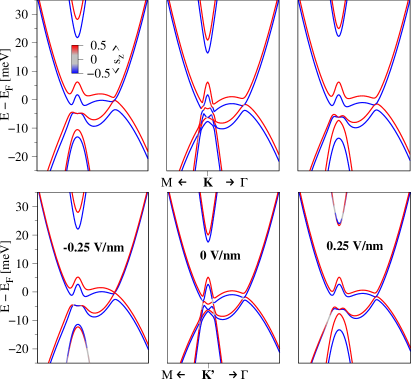
We start our discussion by considering the dispersion of the MoSe2/ABA-TLG/WSe2 heterostructure, see Fig. 7(a). We find that the ABA TLG band structure, featuring the aforementioned 12 energy bands near the point, is nicely preserved within this heterostructure. Here, we are mainly interested in the 8 low-energy bands, see Fig. 7(b), which resemble a combination of single- and bilayer-graphene low-energy spectra. Similar to BLG, the parabolic high-energy bands located at around eV are mainly formed by states from dimer atoms A1, B2, and A3 (see Fig. 21 in appendix D) and are split-off from the Fermi level due to the interlayer hopping . The low-energy bands are mainly formed by the non-dimer atoms B1, A2, and B3, but one of them also contains contributions from A1 and A3 atoms.
The band structure and spin expectation values, see Fig. 7(b,c), are nicely fitted by our model Hamiltonian employing the parameters in Table 1. The proximity-induced SOC parameters are also as expected, giving valley-Zeeman and opposite Rashba couplings for top and bottom graphene layers. Because the bottom graphene layer couples to MoSe2, the values of the corresponding SOC parameters ( and ) are smaller compared to the values for the top graphene layer, which couples to WSe2. This result is in agreement with findings from single-layer-graphene/TMDC heterostructures Gmitra et al. (2016). In addition, the middle layer experiences no proximity SOC, in agreement to BLG/TMDC results Zollner et al. (2020b), where only adjacent layers are proximitized. The two Rashba SOCs are opposite, because the bottom (top) graphene effectively feels the presence of a strong spin-orbit substrate (capping) layer, leading to opposite distortion of the corresponding orbitals.
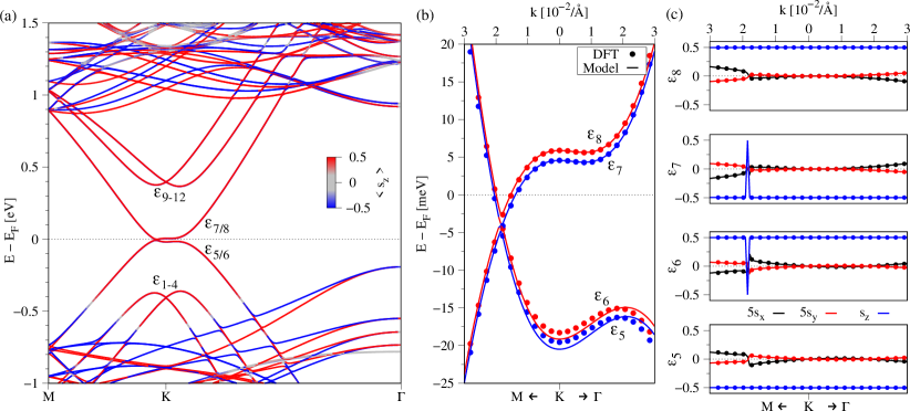
V.1.2 MoSe2/ABC-TLG/WSe2 stacks
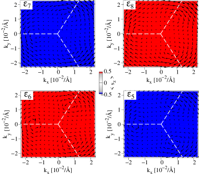
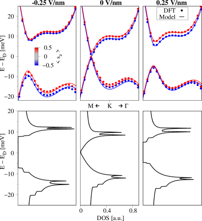
Next, we analyze the dispersion of the MoSe2/ABC-TLG/WSe2 heterostructure, see Fig. 8(a). Again, the bands near the point closely resemble the ones from bare ABC-stacked TLG, but now with proximity SOC due to the surrounding TMDC layers. In contrast to ABA TLG, here we have 8 high-energy bands at around eV, which are again formed by the dimer atoms in the structure, i. e., by the atoms A1, A2, B2, and B3 (see Fig. 22 in Appendix D). The remaining 4 low-energy bands are formed by non-dimer atoms B1 and A3, which are coupled by the hopping . In addition, they feature a cone-like band touching along the direction. Again, the bands and spin expectation values can be nicely reproduced by our model, see Fig. 8(b,c), employing the fit parameters from Table 1. Similar to BLG, the low-energy bands of ABC TLG can be strongly tuned by an electric field (in terms of band gap, see Fig. 4) Konschuh (2011), since only two sublattice atoms from different layers contribute. The electric field tunability of the heterostructure dispersion will be investigated later. Similar to the ABA heterostructure, proximity-induced SOCs are of valley-Zeeman type and the outermost layers experience opposite Rashba couplings. The spin-orbit fields (see Fig. 9), corresponding to the low-energy bands , are mainly polarized, but show a Rashba texture especially around the cone-like touching points along direction. The band touching should actually determine the Fermi level. However in Fig. 8, we have a small amount of doping (), due to the finite -point sampling of the Brillouin zone in the DFT calculation. We therefore fix from the DFT, before we apply our fitting procedure.
V.2 TLG encapsulated within magnetic Cr2Ge2Te6
We now turn to proximity exchange, and consider TLG in ABA and ABC stacking encapsulated by the ferromagnetic semiconductor CGT. Again, the outermost graphene layers will experience proximity couplings, now stemming from the exchange interaction. In general, top and bottom graphene layers can feel different exchange fields. We investigate both parallel and antiparallel magnetizations of the encapsulating CGT layers and analyze the consequences for the TLG low-energy bands.
V.2.1 CGT/ABA/CGT stacks
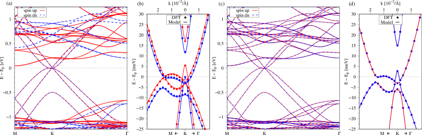
We first address the ABA TLG, sandwiched between two CGT layers. In Fig. 10(a) we show the calculated global band structure of the CGT/ABA-TLG/CGT heterostructure for parallel CGT magnetizations. Especially the ABA TLG low-energy bands can be nicely recognized near the Fermi level. The high-energy conduction bands of TLG are located within the CGT conduction bands. In addition, we find spin-polarized bands close to the Fermi level near the point, originating from the CGT layers. Zooming in on the Fermi level near the point, we again recognize the 8 low-energy bands originating from ABA TLG, see Fig. 10(b). Similar to the TMDC encapsulation, the bands are also significantly split, but now due to the exchange coupling originating from the ferromagnetic CGT layers. The bands can be nicely reproduced by our model Hamiltonian employing the fit parameters listed in Table 1. In general, orbital parameters are barely affected by the surrounding materials proximitizing TLG, as can be seen by comparing with the fit results from the TMDC encapsultion. However, proximity-induced exchange couplings, , are now necessary to capture the essential band structure features. From the fit, we find uniform exchange parameters of about meV for all C sublattice atoms of the two outer graphene layers. This is in agreement with previous considerations for encapsulated BLG Zollner and Fabian (2021c); Zollner et al. (2020b).
What happens if we switch the magnetization direction of one CGT layer? In Fig. 10(c), we show the calculated global band structure of the CGT/ABA-TLG/CGT heterostructure for antiparallel CGT magnetizations. In general, the band structure remains the same, but bands originating from the topmost CGT layer have switched their spin-polarization. Most important are the consequences for the TLG low-energy bands, see Fig. 10(d). For parallel magnetizations, the bands were spin split due to uniform proximity-induced exchange couplings. By switching the magnetization direction of the top CGT layer, the proximity exchange of the topmost graphene layer also adapts and switches sign, as reflected in the fitted parameters, see Table 1. Since the low-energy bands of TLG are equally formed by carbon atoms from top and bottom graphene layers, now with opposite proximity exchange couplings which effectively cancel each other, the bands remain spin degenerate. Again, this is similar as in CGT encapsulated BLG Zollner and Fabian (2021c).
V.2.2 CGT/ABC/CGT stacks
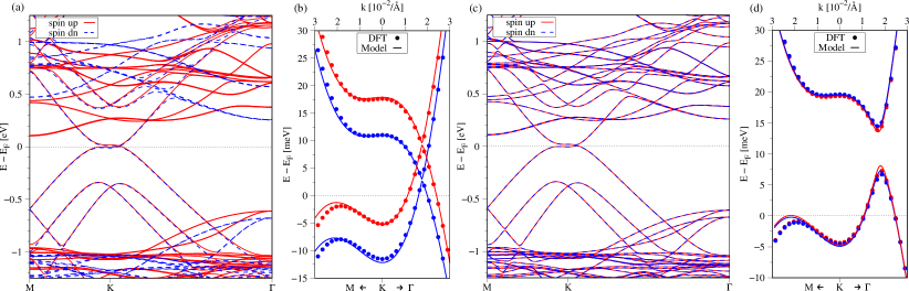
Now, we turn to the CGT encapsulated ABC heterostructure. The band structure and fit results are summarized in Fig. 11, again considering parallel or antiparallel magnetizations of the CGT layers. The low-energy bands of ABC TLG are located near the Fermi level, similar to the TMDC encapsulation. The touching point of the bands is now along the direction, see Fig. 11(b). In contrast, for the TMDC-encapsulated case, the touching was along the direction, see Fig. 8(b). This is related to the different supercell sizes of ABC TLG in the different encapsulation scenarios, and the backfolding of the graphene points into the heterostructure Brillouin zone Zhou et al. (2013). A similar observation can be made considering the ABA TLG band structures for the different encapsulations. Actually, the touching point should determine the Fermi level, but due to the finite -point sampling in our DFT calculation a small doping of about 5 meV appears.
Most important is the low-energy band structure, featuring 4 Dirac-like bands, see Fig. 11(b). In the parallel magnetization case, the bands are split due to uniform proximity-induced exchange coupling in the outermost graphene layers of ABC TLG. The model parameters from Table 1 perfectly reproduce the dispersion in the vicinity of the point, featuring exchange parameters of about meV. Looking at the fitted orbital parameters, we find that and have the opposite sign, but are nearly equal in value, compared to the TMDC-encapsulated ABC structure. This is again related to the different supercells and the backfolding, as already explained.
What happens when we switch the magnetization direction of one CGT layer? In the antiparallel case, see Fig. 11(c,d), the overall band structure is similar to the parallel magnetization. Again, bands originating from the topmost CGT layer have switched their spin-polarization. Most important are the consequences for the ABC TLG low-energy bands. They remain nearly spin degenerate, since the proximity exchange couplings from top and bottom graphene layer are again opposite in sign but nearly equal in value. In addition, a sizable gap opens at the former touching point, which originates from the layered antiferromagnetic proximity exchange in the outermost graphene layers of ABC TLG. This is similar to the observations we made in CGT encapsulated BLG Zollner and Fabian (2021c), where cancellation of proximity exchange or proximity SOC leads to a gap opening without an external electric field. Therefore, also in the TMDC encapsulated scenario, we could open the gap if proximity SOCs from top and bottom graphene layers are opposite. This happens, for example, when employing the same TMDC layers for the encapsulation of ABC TLG, but with a relative twist angle of between them.
Given the similarity of the low energy physics of BLG and ABC TLG, the recently proposed spin valve device concepts Zhai et al. (2021); Wu et al. (2021); Cardoso et al. (2018), which employ proximitized BLG, should be also applicable to ABC TLG. Most important, since the low energy band splittings depend on the magnetic configuration of the outer magnetic layers, as well as on the applied transverse electric field, one can efficiently control the in-plane conductance in doubly proximitized ABC-TLG.
| system | WSe2 | WSe2 | CGT | CGT | CGT | CGT |
| ABC | ABA | ABC | ABC | ABA | ABA | |
| MoSe2 | MoSe2 | CGT | CGT | CGT | CGT | |
| [eV] | 2.5307 | 2.5482 | 2.5048 | 2.5200 | 2.5412 | 2.5375 |
| [eV] | 0.4014 | 0.4028 | 0.3899 | 0.3898 | 0.3612 | 0.3585 |
| [eV] | 0 | -0.0119 | 0 | 0 | -0.0099 | -0.0101 |
| [eV] | 0.3292 | 0.3102 | -0.3287 | -0.3341 | -0.2926 | -0.2926 |
| [eV] | -0.1838 | -0.1765 | -0.1755 | -0.1778 | -0.1723 | -0.1727 |
| [eV] | 0 | 0.0181 | 0 | 0 | 0.0076 | 0.0049 |
| [eV] | 0.0125 | 0 | -0.0113 | -0.0116 | 0 | 0 |
| [meV] | 0.027 | 0.077 | 0.116 | -0.170 | -0.530 | -0.076 |
| [meV] | -11.022 | -6.278 | -12.045 | -7.469 | -3.264 | -2.952 |
| [meV] | 7.961 | 22.084 | 11.095 | 6.937 | 10.162 | 7.583 |
| [meV] | -3.121 | 6.572 | -2.831 | -3.076 | 4.494 | 4.484 |
| [meV] | 0.233 | 0.215 | 0 | 0 | 0 | 0 |
| [meV] | -0.475 | -0.459 | 0 | 0 | 0 | 0 |
| [meV] | 0.209 | 0.204 | 0 | 0 | 0 | 0 |
| [meV] | -0.204 | -0.206 | 0 | 0 | 0 | 0 |
| [meV] | 1.125 | 0.995 | 0 | 0 | 0 | 0 |
| [meV] | -0.983 | -1.011 | 0 | 0 | 0 | 0 |
| [meV] | 0 | 0 | -3.393 | -3.393 | -3.210 | -3.210 |
| [meV] | 0 | 0 | -3.393 | -3.393 | -3.210 | -3.210 |
| [meV] | 0 | 0 | -3.349 | 3.349 | -3.210 | 3.210 |
| [meV] | 0 | 0 | -3.349 | 3.349 | -3.210 | 3.210 |
| [meV] | -4.171 | 0 | 5.540 | 10.605 | 0 | 0 |
| dipole [debye] | -0.0152 | -0.0109 | -0.0110 | 0.0010 | 0.0087 | 0.0101 |
VI Electric Field Tunability
Finally, we consider the electric field tunability of the low-energy bands of encapsulated TLG. The main effect of the field is that we place the outermost graphene layers in different potentials, thereby opening band gaps in the spectrum; see for example Fig. 4 for bare ABC TLG. In the following, we restrict ourselves to the case of TMDC encapsulation, since for the CGT case one can expect similar outcomes. More precisely, as we have seen above, the most striking difference between the CGT and TMDC encapsulation cases is that proximity exchange coupling, rather than proximity SOC, is responsible for the band splittings. From the model Hamiltonian perspective, see Table 1, orbital parameters are barely different for the two encapsulation scenarios, while proximity exchange couplings, , are about 3-times larger in magnitude compared to proximity SOCs, . Therefore, one can expect a similar electric field behavior of the TLG low energy bands in both encapsulations. In addition, below we restrict ourselves to consider small field values of 0.25 V/nm, to capture the main effects of the field on the dispersion. In Fig. 5, we specify the direction of a positive electric field.
VI.1 MoSe2/ABC-TLG/WSe2 stacks
In Fig. 12 we show the electric field evolution of the MoSe2/ABC-TLG/WSe2 low-energy bands, including model fits. Since our model Hamiltonian very accurately reproduces the low-energy dispersions, we also show the corresponding DOS, calculated from the model dos . When an electric field is applied across ABC TLG, a band gap opens at the cone-like band touching along the line. The field separates the outer graphene layers in energy by the potential . In order to fit the low-energy bands, when an electric field is applied, we keep the parameters from Table 1 fixed, but refit the parameters and . The reason is that the applied field is small ( V/nm) and especially these two orbital parameters are relevant for the atoms B1 and A3, forming the low-energy bands. With this approach, the band structures with electric field are almost perfectly reproduced by the model.
In addition, we note that for negative field, the conduction band is split much less than the valence band and vice versa for the positive field. This can be also seen by looking at the calculated DOS. Such a switching of band splittings reminds us of the BLG physics Gmitra and Fabian (2017); Zollner et al. (2020b); Island et al. (2019); Zollner and Fabian (2021c). As theoretically proposed Gmitra and Fabian (2017) and experimentally demonstrated Island et al. (2019), a transverse electric field, applied across a BLG/TMDC heterostructure, can efficiently tune SOC of conduction electrons, making it a potential platform for a spin-transistor. For ABC TLG, the low-energy bands are formed by atoms B1 and A3, which experience different magnitudes of proximity SOC, as the corresponding spin-orbit parameters in Table 1 show. For positive electric field, the bottom graphene layer, which couples to MoSe2, sits in a lower potential than the top graphene layer, which couples to WSe2. Therefore, the valence band is mainly formed by atoms B1, experiencing proximity SOC of about 0.2 meV, while the conduction band is formed by atoms A3, having proximity SOC of about 1 meV. For negative electric field, the situation is reversed allowing to fully electrically swap between the two magnitudes of SOC in the low-energy bands of ABC TLG. Such a swapping between spin-orbit splittings allows to electrically control spin relaxation in proximitized ABC TLG.
VI.2 MoSe2/ABA-TLG/WSe2 stacks

The impact of a transverse electric field on the ABA bands and DOS is more complicated than for the ABC case, see Fig. 13. Here, we have 8 low-energy bands that are present near the Fermi level, and which are formed by almost all carbon atoms from the three layers. Nevertheless, similar to ABC TLG, the electric field introduces a potential difference between the outermost graphene layers. In the model Hamiltonian, we capture this with parameter . In addition, the middle layer can in general also sit in some nonzero potential, that we capture by . Therefore, in order to fit the bands when an electric field is applied, we fix the parameters from Table 1, but refit the parameters and . Again, the band structures with electric field are also nicely reproduced by the model Hamiltonian, allowing us to calculate the DOS dos .
With the small field amplitudes that we employ, the low-energy dispersion barely changes. Nevertheless, the Dirac-like bands are further separated in energy and now strongly anticross with the BLG-like bands. The parabolic bands still touch along the direction and the spectrum is not yet gapped for fields of V/nm, as can be seen from the DOS.
VII Interplay of spin interactions
One important conclusion of the previous discussion is that one can very well reproduce DFT data with our model Hamiltonians. The inclusion of an electric field, transverse to the monolayers, is straightforward, as it can be parametrized by essentially two orbital parameters. Considering also that the proximity effects are short ranged, we can realistically study more complex structures, such as ex-so-tic CGT/TLG/TMDC heterostructures exs .
To be specific, we investigate TLG encapsulated by strong spin-orbit semiconductor WSe2 on the top, and ferromagnetic semiconductor CGT on the bottom. To calculate the dispersion from the model Hamiltonian, we use the orbital parameters from Table 1 of TMDC-encapsulated ABA and ABC TLG. In addition, we employ valley Zeeman and Rashba SOC for the top graphene layer ( meV, meV), as well as exchange coupling for the bottom graphene layer ( meV). This is a reasonable choice, according to our findings. To study the electric field behavior, also on the model level, we additionally employ the fitted parameters for the different electric fields ( and for ABA; and for ABC), see Fig. 12 and Fig. 13. The combination of SOC and proximity exchange breaks time-reversal symmetry. Therefore, we calculated the dispersion near both the and valleys.
VII.1 ABC
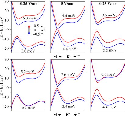
The model results for ABC TLG are summarized in Fig. 14. For zero field, both sublattice atoms B1 and A3 are equally contributing to all four low-energy bands. The band splittings result now from the interplay of proximity spin-orbit and exchange couplings, originating from the individual layers. Consequently, at (), the two spin interactions are additive (subtractive) and band splittings are about 4.5 meV (2.5 meV). Moreover, we find that the ABC low-energy bands exhibit no gap near valley, while there is a gap near valley, see Fig. 14, potentially important for the realization of a valley-polarized quantum anomalous Hall effect Vila et al. (2021).
When an electric field is introduced, the bands are separated in energy, since the outermost layers are now in different potentials. In addition, the bands are not anymore equally formed by the two sublattice atoms. Still, the different spin interactions are at interplay, either in an additive or subtractive way. Consequently, for positive field both bands are spin split at , while at the valence band is strongly split and the conduction band stays nearly degenerate. Reversing the direction of the electric field, the bands are flipped with respect to the Fermi level, since also the potential difference is now opposite compared to the positive field. The fact that different magnitudes of splittings arise in different bands and valleys is important for the gate control of spin-relaxation Gmitra and Fabian (2017), potentially resulting in valley- and spin-polarized currents Vila et al. (2021).
VII.2 ABA
In Fig. 15, we show the calculated model low-energy dispersion of the ABA TLG, when the two spin interactions are at interplay. For zero field, we observe a similar behavior as for the ABC TLG, where near the band splittings are larger than near , due to additive/subtractive effects of the spin interactions. In addition, looking at the field evolution ( V/nm) of the Dirac-like bands, we observe a swapping of the nearly spin-degenerate bands from valence into conduction side at the valley, and vice versa for the strongly split bands. Similar observations can be made at the valley. The BLG-like parabolic bands remain more or less the same with the applied field.
VIII Summary
We have investigated systematically the electronic band structure of TLG in different stacking and encapsulation configurations. Starting with bare ABA, ABC, and ABB TLG, we have provided the essential ingredients of the orbital and spin-orbital effects, and both quantitative and qualitative understanding of the SOC at the sub-meV level. Important for ongoing investigations, we also report on the electric-field tunability of the electronic DOS and VHS.
The bulk of our investigation is devoted to encapsulated TLG. We deal separately with proximity SOC and proximity exchange. The proximity SOC is studied by encapsulating ABA and ABC TLG within WSe2 and MoSe2. We show how the two semiconducting monolayers affect the low-energy bands of TLG, inducing relatively strong (meV) spin splittings that are tunable by electric field. We also show that the effective model Hamiltonian, which considers sizeable SOC on the outer layers, performs great in explaining the DFT results.
Proximity exchange is analyzed for the stacks of TLG encapsulated within CGT monolayers. The proximity exchange, also on meV scale, modifies the low-energy bands of TLG, differently for parallel and antiparallel CGT magnetizations. The magnetic tunability should be a useful way to control correlated phases, especially in ABC TLG which exhibits a large DOS at low energies.
The nice comparison between the DFT results and the model makes us confident in applying the model itself in more complex situations, such as studying ex-so-tic CGT/TLG/TMDC heterostructures exs . The interplay of spin-orbit and exchange coupling leads to a different band structure at and . In addition, the layer polarization then allows for a strong tunability of the bands with a transverse electric field, which is able to close or open spin splittings, or even switch the spin polarization, for a particular band in encapsulated ABC TLG.
In all our investigated DFT cases we provide fitting parameters to the effective model as a useful resource for subsequent investigations of transport and correlated physics based on realistic model simulations.
Acknowledgements.
This work was funded by the Deutsche Forschungsgemeinschaft (DFG, German Research Foundation) SFB 1277 (Project No. 314695032), SPP 2244 (Project No. 443416183), and the European Union Horizon 2020 Research and Innovation Program under contract number 881603 (Graphene Flagship). M. G. acknowledges financial support provided by Slovak Research and Development Agency provided under Contract No. APVV-20-0150 and by the Ministry of Education, Science, Research and Sport of the Slovak Republic provided under Grant No. VEGA 1/0105/20.Appendix A Electric field effects of bare ABA and ABC trilayer graphene
| el. field [V/nm] | 0 | 0.25 | 0.5 | 0.75 | 1.0 |
|---|---|---|---|---|---|
| [eV] | 2.5692 | 2.5693 | 2.5695 | 2.5693 | 2.5688 |
| [eV] | 0.3699 | 0.3700 | 0.3700 | 0.3700 | 0.3701 |
| [eV] | -0.0101 | -0.0101 | -0.0100 | -0.0099 | -0.0098 |
| [eV] | 0.2829 | 0.2821 | 0.2798 | 0.2772 | 0.2742 |
| [eV] | -0.1643 | -0.1640 | -0.1638 | -0.1642 | -0.1635 |
| [eV] | 0.0150 | 0.0130 | 0.0129 | 0.0130 | 0.0132 |
| [meV] | 0 | -19.146 | -38.608 | -57.927 | -78.221 |
| [meV] | -19.991 | -14.814 | -13.980 | -13.846 | -14.715 |
| [meV] | 20.566 | 24.193 | 24.452 | 24.158 | 23.983 |
| [meV] | 6.965 | 12.842 | 13.189 | 12.757 | 12.506 |
| dipole [debye] | 0 | 0.0250 | 0.0499 | 0.0749 | 0.0996 |
| el. field [V/nm] | 0 | 0.25 | 0.5 | 0.75 | 1.0 |
|---|---|---|---|---|---|
| [eV] | 2.5539 | 2.5560 | 2.5656 | 2.5884 | 2.6198 |
| [eV] | 0.3690 | 0.3689 | 0.3689 | 0.3687 | 0.3685 |
| [eV] | 0.2917 | 0.2948 | 0.2960 | 0.2905 | 0.2816 |
| [eV] | -0.1646 | -0.1642 | -0.1618 | -0.1571 | -0.1516 |
| [eV] | 0.0108 | 0.0113 | 0.0117 | 0.0115 | 0.0111 |
| [meV] | 0 | -3.050 | -10.124 | -18.172 | -25.409 |
| [meV] | -37.243 | -37.184 | -36.066 | -34.365 | -32.529 |
| [meV] | 10.288 | 9.746 | 9.001 | 9.816 | 9.094 |
| [meV] | -1.121 | -1.551 | -1.664 | 0.172 | 0.467 |
| dipole [debye] | 0 | 0.0286 | 0.0552 | 0.0812 | 0.1077 |

The following electric field results for bare ABA and ABC TLG have been obtained with Quantum ESPRESSO Giannozzi et al. (2009). We used the same structural input as for WIEN2k Blaha et al. (2001), as described in the main text. Self-consistent calculations are performed with the -point sampling of to accurately determine the Fermi level and the DOS. We used an energy cutoff for the charge density of Ry, and the kinetic energy cutoff for wavefunctions is Ry for the scalar relativistic pseudopotentials with the projector augmented wave method Kresse and Joubert (1999) with the Perdew-Burke-Ernzerhof exchange correlation functional Perdew et al. (1996). Moreover, we added vdW Grimme (2006); Barone et al. (2009) and dipole corrections Bengtsson (1999).
Since we are mainly interested in the electric field behavior of the dispersion and the DOS, we neglect SOC, since the induced splittings are on the eV level (see main text). In any case, the plane wave and pseudopotential method, implemented in Quantum ESPRESSO Giannozzi et al. (2009), cannot give correct spin-orbit splittings in graphene, since the relevant -orbitals are missing Gmitra et al. (2009); Konschuh et al. (2010). Nevertheless, on an orbital level, the dispersions are the same as calculated with WIEN2k Blaha et al. (2001), and we can safely study the electric field tunability.
The fit parameters from Table 2 and Table 3, nicely reproduce the DFT-calculated band structures in Fig. 4 for ABC TLG and Fig. 16 for ABA TLG, employing the orbital model Hamiltonians, and , from the main text. The electric field behaviour of the ABC TLG dispersion and DOS was already discussed in the main text. For the ABA TLG, the electric field also introduces a potential difference between the outermost layers, separating the monolayer graphene bands in energy. The BLG bands stay more or less the same with the applied field, see Fig. 16. In addition, a small band gap is introduced at the Fermi level. However, the gap first increases and then decreases again, when tuning the field from 0 to 1 V/nm. From the DOS, we find VHS associated with the parabolic BLG bands. With increasing field, we find that these bands even further flatten near the Fermi level, which comes along with increasing VHS in the DOS.
The fitted electric field results, summarized in Table 2 and Table 3 are valuable for further theoretical considerations, e. g., gate-tunable transport simulations of bare ABA and ABC TLG. If one wants to add SOC, this can be easily done on a model level, employing the intrinsic SOC of bare graphene, eV, for all sublattice atoms Gmitra et al. (2009); Konschuh et al. (2010). The Rashba SOC would be even smaller (at maximum 5 eV) for our investigated field values Konschuh (2011); Konschuh et al. (2012). Certainly, one can also add proximity spin-orbit or exchange couplings, as we describe it for our encapsulated structures.
Appendix B Bare ABB trilayer graphene
In addition to ABA and ABC TLG, there is also another stacking sequence, the ABB one. All those stackings are present in recent investigations on twisted-graphene/BLG heterostructures Polshyn et al. (2020); Rademaker et al. (2020); Park et al. (2020); Ma et al. (2021). In the same manner as above and in the main text, we calculated the dispersion, DOS, and analyze the electric field behavior of ABB TLG. A reasonable orbital Hamiltonian for ABB TLG can be constructed from combining the knowledge about AA and AB stacked BLG, together with the ABC and ABA TLG Konschuh et al. (2012); Konschuh (2011); Rakhmanov et al. (2012); Rozhkov et al. (2016). We propose the following ABB TLG orbital Hamiltonian
| (5) |
| el. field [V/nm] | 0 | 0.25 | 0.5 | 0.75 | 1.0 |
|---|---|---|---|---|---|
| [eV] | 2.5662 | 2.5682 | 2.5713 | 2.5737 | 2.5754 |
| [eV] | 0.3698 | 0.3697 | 0.3693 | 0.3687 | 0.3683 |
| [eV] | 0.2726 | 0.2723 | 0.2716 | 0.2706 | 0.2694 |
| [eV] | -0.1716 | -0.1699 | -0.1722 | -0.1760 | -0.1793 |
| [eV] | 0.0229 | 0.0228 | 0.0246 | 0.0264 | 0.0275 |
| [eV] | -0.1087 | -0.1101 | -0.1053 | -0.0966 | -0.0874 |
| [meV] | 0 | -12.982 | -31.824 | -48.449 | -64.292 |
| [meV] | -51.533 | -53.755 | -60.330 | -66.823 | -71.386 |
| [meV] | 21.367 | 21.737 | 20.917 | 19.660 | 18.542 |
| dipole [debye] | 0 | 0.0245 | 0.0500 | 0.0764 | 0.1029 |

A schematic illustration of the couplings in ABB TLG is shown in Fig. 17. The hoppings between the bottom and middle graphene layer are the same as for the other TLG structures. However, the hoppings between the middle and the top graphene layer are adapted from the AA BLG structure Rozhkov et al. (2016). Since the ABB TLG has no -mirror or inversion symmetry, connecting the top and bottom layer, the direct interlayer hoppings and can be in principle different. Only when the interlayer distances are the same, also the hopping amplitudes are the same. The coupling , connecting opposite sublattices from different layers, is similar to the coupling , connecting same sublattices from different layers. Nevertheless, they can be very different in amplitude.
The pseudospin character and the spin-orbit splittings in the bare ABB TLG dispersion have been already discussed in the main text. In Fig. 18, we show a zoom to the ABB TLG low-energy bands, further emphasizing the effect of a transverse electric field on the dispersion and the spin splittings. Applying the field, apparently flips the low-energy band splittings at the point with respect to the Fermi level. This is not surprising, considering the projected band structure in Fig. 3(c). Without the field, the low-energy conduction (valence) band has a pronounced contribution from B1 (B3) atoms near the anticrossing points away from . With the electric field, applied along positive direction, a potential difference between the outermost layers is introduced, such that the bottom layer is now in the lowest potential. Therefore, the band characters of valence and conduction bands flip, along with the spin splittings near the point.
Appendix C Effects of relaxation on bare TLG dispersions
In the main text, when discussing bare TLG, we have fixed the interlayer distances between the graphene layers to Å, which is an approximation. We now allow the TLG structures to minimize their energy by relaxing the C atom positions. For the relaxation we employ DFT-D2 vdW corrections Grimme (2006); Barone et al. (2009) and use quasi-newton algorithm based on trust radius procedure. To determine the interlayer distances, the carbon atoms are allowed to relax only in their positions (vertical to the layers), until all components of all forces are reduced below [Ry/], where is the Bohr radius.
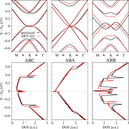
After relaxation, interlayer distances are slightly reduced to about Å. The only exception is the interlayer distance between BB-layers in ABB TLG, which is relaxed to about Å. With the relaxed interlayer distances it is now also reasonable to compare the total energies of all the stackings. We find that the ABA TLG is energetically most favorable. However, the ABC one is only about eV higher in energy. The ABB TLG is 25 meV higher in energy than the ABA one, making this stacking less favorable to be observed naturally. In Fig. 20, we compare the band structure and DOS results for the TLG structures with and without the relaxation. The most drastic changes can be seen in the ABB TLG dispersion, since interlayer distances are now highly asymmetric. For the ABC and ABA TLG structures, the dispersion is barely different, except for the high-energy bands.
| TLG | ABC | ABA | ABB |
|---|---|---|---|
| [eV] | 2.5470 | 2.5687 | 2.5845 |
| [eV] | 0.4103 | 0.4128 | 0.4133 |
| [eV] | - | - | 0.2593 |
| [eV] | - | -0.0067 | - |
| [eV] | 0.3243 | 0.3128 | 0.2755 |
| [eV] | -0.1794 | -0.1954 | -0.2018 |
| [eV] | - | 0.0089 | 0.0167 |
| [eV] | 0.0133 | - | - |
| [eV] | - | - | -0.0077 |
| [meV] | 0 | 0 | 0 |
| [meV] | -45.161 | -20.831 | -27.767 |
| [meV] | 11.105 | 31.501 | 9.040 |
| [meV] | -2.838 | 5.069 | - |
In Table 5, we summarize the fit results, when the structures are relaxed. Especially the direct interlayer couplings and are strongly renormalized, because of the different interlayer distances. The high-energy bands are split off exactly due to these couplings, explaining the differences in the dispersions with and without relaxation.
Appendix D Pseudospin character of TMDC encapsulated TLG dispersions
In Fig. 21, we show the pseudospin character of the relevant ABA TLG bands of the TMDC encapsulated heterostructure. Similar as in Fig. 1, the parabolic BLG-like bands are formed by atoms B1, A2, and B3, which form the non-dimer interlayer pairs. The Dirac bands are formed by orbitals from the outermost graphene layers.
In Fig. 22, we show the pseudospin character of the ABC TLG bands of the TMDC encapsulated heterostructure. Consistent with Fig. 2, the flat low-energy bands are formed by the outer-layer atoms B1 and A3, while high-energy bands are formed by all other atoms.
References
- Han et al. (2014) Wei Han, Roland K Kawakami, Martin Gmitra, and Jaroslav Fabian, “Graphene spintronics,” Nat. Nanotechnol. 9, 794 (2014).
- Fabian et al. (2007) Jaroslav Fabian, Alex Matos-Abiague, Christian Ertler, Peter Stano, and Igor Zutic, “Semiconductor spintronics,” Acta Phys. Slov. 57, 565 (2007).
- Gong and Zhang (2019) Cheng Gong and Xiang Zhang, “Two-dimensional magnetic crystals and emergent heterostructure devices,” Science 363, eaav4450 (2019).
- Li et al. (2019) Hui Li, Shuangchen Ruan, and Yu‐Jia Zeng, “Intrinsic Van Der Waals Magnetic Materials from Bulk to the 2D Limit: New Frontiers of Spintronics,” Adv. Mater. 31, 1900065 (2019).
- Cortie et al. (2019) David L. Cortie, Grace L. Causer, Kirrily C. Rule, Helmut Fritzsche, Wolfgang Kreuzpaintner, and Frank Klose, “Two‐Dimensional Magnets: Forgotten History and Recent Progress towards Spintronic Applications,” Adv. Funct. Mater. 30, 1901414 (2019).
- Zutic et al. (2019) Igor Zutic, Alex Matos-Abiague, Benedikt Scharf, Hanan Dery, and Kirill Belashchenko, “Proximitized materials,” Mater. Today 22, 85 (2019).
- Sierra et al. (2021) Juan F. Sierra, Jaroslav Fabian, Roland K. Kawakami, Stephan Roche, and Sergio O. Valenzuela, “Van der waals heterostructures for spintronics and opto-spintronics,” Nature Nanotechnology 16, 856–868 (2021).
- Li et al. (2020) Jing Li, Han-Bing Leng, Hailong Fu, Kenji Watanabe, Takashi Taniguchi, Xin Liu, Chao-Xing Liu, and Jun Zhu, “Superconducting proximity effect in a transparent van der waals superconductor-metal junction,” Phys. Rev. B 101, 195405 (2020).
- Moriya et al. (2020) Rai Moriya, Naoto Yabuki, and Tomoki Machida, “Superconducting proximity effect in a van der waals junction,” Phys. Rev. B 101, 054503 (2020).
- Trainer et al. (2020) Daniel J Trainer, BaoKai Wang, Fabrizio Bobba, Noah Samuelson, Xiaoxing Xi, John Zasadzinski, Jouko Nieminen, Arun Bansil, and Maria Iavarone, “Proximity-induced superconductivity in monolayer mos2,” ACS nano 14, 2718–2728 (2020).
- Zollner et al. (2016) Klaus Zollner, Martin Gmitra, Tobias Frank, and Jaroslav Fabian, “Theory of proximity-induced exchange coupling in graphene on hBN/(Co, Ni),” Phys. Rev. B 94, 155441 (2016).
- Zollner et al. (2018) Klaus Zollner, Martin Gmitra, and Jaroslav Fabian, “Electrically tunable exchange splitting in bilayer graphene on monolayer Cr2X2Te6 with X = Ge, Si, and Sn,” New J. Phys. 20, 073007 (2018).
- Zollner et al. (2019a) Klaus Zollner, Paulo E. Faria Junior, and Jaroslav Fabian, “Proximity exchange effects in and heterostructures with : Twist angle, layer, and gate dependence,” Phys. Rev. B 100, 085128 (2019a).
- Zollner et al. (2020a) Klaus Zollner, Paulo E. Faria Junior, and Jaroslav Fabian, “Giant proximity exchange and valley splitting in transition metal dichalcogenide//(Co, Ni) heterostructures,” Phys. Rev. B 101, 085112 (2020a).
- Zhang et al. (2015) Jiayong Zhang, Bao Zhao, Yugui Yao, and Zhongqin Yang, “Robust quantum anomalous Hall effect in graphene-based van der Waals heterostructures,” Phys. Rev. B 92, 165418 (2015).
- Zhang et al. (2018) Jiayong Zhang, Bao Zhao, Tong Zhou, Yang Xue, Chunlan Ma, and Zhongqin Yang, “Strong magnetization and Chern insulators in compressed van der Waals heterostructures,” Phys. Rev. B 97, 085401 (2018).
- Vila et al. (2021) Marc Vila, Jose H. Garcia, and Stephan Roche, “Valley-polarized quantum anomalous hall phase in bilayer graphene with layer-dependent proximity effects,” Phys. Rev. B 104, L161113 (2021).
- Wang et al. (2015) Zhiyong Wang, Chi Tang, Raymond Sachs, Yafis Barlas, and Jing Shi, “Proximity-Induced Ferromagnetism in Graphene Revealed by the Anomalous Hall Effect,” Phys. Rev. Lett. 114, 016603 (2015).
- Xu et al. (2018) Lei Xu, Ming Yang, Lei Shen, Jun Zhou, Tao Zhu, and Yuan Ping Feng, “Large valley splitting in monolayer by proximity coupling to an insulating antiferromagnetic substrate,” Phys. Rev. B 97, 041405 (2018).
- Yang et al. (2013) H. X. Yang, A. Hallal, D. Terrade, X. Waintal, S. Roche, and M. Chshiev, “Proximity Effects Induced in Graphene by Magnetic Insulators: First-Principles Calculations on Spin Filtering and Exchange-Splitting Gaps,” Phys. Rev. Lett. 110, 046603 (2013).
- Zhong et al. (2020) Ding Zhong, Kyle L. Seyler, Xiayu Linpeng, Nathan P. Wilson, Takashi Taniguchi, Kenji Watanabe, Michael A. McGuire, Kai-Mei C. Fu, Di Xiao, Wang Yao, and Xiaodong Xu, “Layer-resolved magnetic proximity effect in van der Waals heterostructures,” Nat. Nanotechnol. 15, 187 (2020).
- Averyanov et al. (2018) Dmitry V Averyanov, Ivan S Sokolov, Andrey M Tokmachev, Oleg E Parfenov, Igor A Karateev, Alexander N Taldenkov, and Vyacheslav G Storchak, “High-Temperature Magnetism in Graphene Induced by Proximity to EuO,” ACS Appl. Mater. Interfaces 10, 20767 (2018).
- Ciorciaro et al. (2020) Livio Ciorciaro, Martin Kroner, Kenji Watanabe, Takashi Taniguchi, and Atac Imamoglu, “Observation of magnetic proximity effect using resonant optical spectroscopy of an electrically tunable heterostructure,” Phys. Rev. Lett. 124, 197401 (2020).
- Gmitra and Fabian (2015) Martin Gmitra and Jaroslav Fabian, “Graphene on transition-metal dichalcogenides: A platform for proximity spin-orbit physics and optospintronics,” Phys. Rev. B 92, 155403 (2015).
- Gmitra et al. (2016) Martin Gmitra, Denis Kochan, Petra Högl, and Jaroslav Fabian, “Trivial and inverted Dirac bands and the emergence of quantum spin Hall states in graphene on transition-metal dichalcogenides,” Phys. Rev. B 93, 155104 (2016).
- Zollner and Fabian (2019) Klaus Zollner and Jaroslav Fabian, “Single and bilayer graphene on the topological insulator : Electronic and spin-orbit properties from first principles,” Phys. Rev. B 100, 165141 (2019).
- Zollner and Fabian (2021a) Klaus Zollner and Jaroslav Fabian, “Heterostructures of graphene and topological insulators bi2se3, bi2te3, and sb2te3,” physica status solidi (b) 258, 2000081 (2021a).
- Song et al. (2018) Kenan Song, David Soriano, Aron W. Cummings, Roberto Robles, Pablo Ordejón, and Stephan Roche, “Spin Proximity Effects in Graphene/Topological Insulator Heterostructures,” Nano Lett. 18, 2033 (2018).
- Zhang et al. (2014) Junhua Zhang, C. Triola, and E. Rossi, “Proximity Effect in Graphene-Topological-Insulator Heterostructures,” Phys. Rev. Lett. 112, 096802 (2014).
- Avsar et al. (2017) Ahmet Avsar, Dmitrii Unuchek, Jiawei Liu, Oriol Lopez Sanchez, Kenji Watanabe, Takashi Taniguchi, Barbaros Özyilmaz, and Andras Kis, “Optospintronics in Graphene via Proximity Coupling,” ACS Nano 11, 11678 (2017).
- Avsar et al. (2014) A Avsar, J Y Tan, T Taychatanapat, J Balakrishnan, G. K. W. Koon, Y Yeo, J Lahiri, A Carvalho, A S Rodin, E. C. T. O’Farrell, G Eda, A H Castro Neto, and B. Özyilmaz, “Spin–orbit proximity effect in graphene,” Nat. Commun. 5, 4875 (2014).
- Alsharari et al. (2018) Abdulrhman M. Alsharari, Mahmoud M. Asmar, and Sergio E. Ulloa, “Proximity-induced topological phases in bilayer graphene,” Phys. Rev. B 97, 241104 (2018).
- Frank et al. (2016) Tobias Frank, Martin Gmitra, and Jaroslav Fabian, “Theory of electronic and spin-orbit proximity effects in graphene on Cu(111),” Phys. Rev. B 93, 155142 (2016).
- David et al. (2019) Alessandro David, Péter Rakyta, Andor Kormányos, and Guido Burkard, “Induced spin-orbit coupling in twisted graphene–transition metal dichalcogenide heterobilayers: Twistronics meets spintronics,” Phys. Rev. B 100, 085412 (2019).
- Ghiasi et al. (2019) Talieh S Ghiasi, Alexey A Kaverzin, Patrick J Blah, and Bart J van Wees, “Charge-to-Spin Conversion by the Rashba–Edelstein Effect in Two-Dimensional van der Waals Heterostructures up to Room Temperature,” Nano Lett. 19, 5959 (2019).
- Benitez et al. (2020) L Antonio Benitez, Williams Savero Torres, Juan F Sierra, Matias Timmermans, Jose H Garcia, Stephan Roche, Marius V Costache, and Sergio O Valenzuela, “Tunable room-temperature spin galvanic and spin Hall effects in van der Waals heterostructures,” Nat. Mater. 19, 170 (2020).
- Luo et al. (2017) Yunqiu Kelly Luo, Jinsong Xu, Tiancong Zhu, Guanzhong Wu, Elizabeth J. McCormick, Wenbo Zhan, Mahesh R. Neupane, and Roland K. Kawakami, “Opto-valleytronic spin injection in monolayer MoS2/few-layer graphene hybrid spin valves,” Nano Lett. 17, 3877 (2017).
- Safeer et al. (2019) CK Safeer, Josep Ingla-Aynés, Franz Herling, José H Garcia, Marc Vila, Nerea Ontoso, M Reyes Calvo, Stephan Roche, Luis E Hueso, and Fèlix Casanova, “Room-temperature spin Hall effect in graphene/MoS2 van der Waals heterostructures,” Nano Lett. 19, 1074 (2019).
- Herling et al. (2020) Franz Herling, C. K. Safeer, Josep Ingla-Aynés, Nerea Ontoso, Luis E. Hueso, and Fèlix Casanova, “Gate tunability of highly efficient spin-to-charge conversion by spin hall effect in graphene proximitized with wse2,” APL Materials 8, 071103 (2020).
- Zollner and Fabian (2021b) Klaus Zollner and Jaroslav Fabian, “Engineering proximity exchange by twisting: Reversal of ferromagnetic and emergence of antiferromagnetic dirac bands in graphene/cr2ge2te6,” arXiv:2108.03984 (2021b).
- Naimer et al. (2021) Thomas Naimer, Klaus Zollner, Martin Gmitra, and Jaroslav Fabian, “Twist-angle dependent proximity induced spin-orbit coupling in graphene/transition metal dichalcogenide heterostructures,” Physical Review B 104 (2021), 10.1103/physrevb.104.195156.
- Carr et al. (2017) Stephen Carr, Daniel Massatt, Shiang Fang, Paul Cazeaux, Mitchell Luskin, and Efthimios Kaxiras, “Twistronics: Manipulating the electronic properties of two-dimensional layered structures through their twist angle,” Phys. Rev. B 95, 075420 (2017).
- Hennighausen and Kar (2021) Zachariah Hennighausen and Swastik Kar, “Twistronics: a turning point in 2d quantum materials,” Electronic Structure 3, 014004 (2021).
- Ribeiro-Palau et al. (2018) Rebeca Ribeiro-Palau, Changjian Zhang, Kenji Watanabe, Takashi Taniguchi, James Hone, and Cory R. Dean, “Twistable electronics with dynamically rotatable heterostructures,” Science 361, 690–693 (2018).
- Carr et al. (2020) Stephen Carr, Shiang Fang, and Efthimios Kaxiras, “Electronic-structure methods for twisted moiré layers,” Nature Reviews Materials 5, 748–763 (2020).
- Cao et al. (2018a) Yuan Cao, Valla Fatemi, Shiang Fang, Kenji Watanabe, Takashi Taniguchi, Efthimios Kaxiras, and Pablo Jarillo-Herrero, “Unconventional superconductivity in magic-angle graphene superlattices,” Nature 556, 43 (2018a).
- Cao et al. (2018b) Yuan Cao, Valla Fatemi, Ahmet Demir, Shiang Fang, Spencer L. Tomarken, Jason Y. Luo, Javier D. Sanchez-Yamagishi, Kenji Watanabe, Takashi Taniguchi, Efthimios Kaxiras, Ray C. Ashoori, and Pablo Jarillo-Herrero, “Correlated insulator behaviour at half-filling in magic-angle graphene superlattices,” Nature 556, 80 (2018b).
- Arora et al. (2020) Harpreet Singh Arora, Robert Polski, Yiran Zhang, Alex Thomson, Youngjoon Choi, Hyunjin Kim, Zhong Lin, Ilham Zaky Wilson, Xiaodong Xu, Jiun-Haw Chu, and et al., “Superconductivity in metallic twisted bilayer graphene stabilized by wse2,” Nature 583, 379–384 (2020).
- Stepanov et al. (2020) Petr Stepanov, Ipsita Das, Xiaobo Lu, Ali Fahimniya, Kenji Watanabe, Takashi Taniguchi, Frank HL Koppens, Johannes Lischner, Leonid Levitov, and Dmitri K Efetov, “Untying the insulating and superconducting orders in magic-angle graphene,” Nature 583, 375–378 (2020).
- Lu et al. (2019) Xiaobo Lu, Petr Stepanov, Wei Yang, Ming Xie, Mohammed Ali Aamir, Ipsita Das, Carles Urgell, Kenji Watanabe, Takashi Taniguchi, Guangyu Zhang, et al., “Superconductors, orbital magnets and correlated states in magic-angle bilayer graphene,” Nature 574, 653–657 (2019).
- Sharpe et al. (2019) Aaron L. Sharpe, Eli J. Fox, Arthur W. Barnard, Joe Finney, Kenji Watanabe, Takashi Taniguchi, M. A. Kastner, and David Goldhaber-Gordon, “Emergent ferromagnetism near three-quarters filling in twisted bilayer graphene,” Science 365, 605–608 (2019).
- Gmitra and Fabian (2017) Martin Gmitra and Jaroslav Fabian, “Proximity Effects in Bilayer Graphene on Monolayer WSe2: Field-Effect Spin Valley Locking, Spin-Orbit Valve, and Spin Transistor,” Phys. Rev. Lett. 119, 146401 (2017).
- Amann et al. (2021) Julia Amann, Tobias Völkl, Tobias Rockinger, Denis Kochan, Kenji Watanabe, Takashi Taniguchi, Jaroslav Fabian, Dieter Weiss, and Jonathan Eroms, “Counterintuitive gate dependence of weak antilocalization in bilayer graphene/wse2 heterostructures,” arXiv:2012.05718 (2021).
- Zollner et al. (2020b) Klaus Zollner, Martin Gmitra, and Jaroslav Fabian, “Swapping exchange and spin-orbit coupling in 2d van der waals heterostructures,” Phys. Rev. Lett. 125, 196402 (2020b).
- Lin et al. (2022) Jiang-Xiazi Lin, Ya-Hui Zhang, Erin Morissette, Zhi Wang, Song Liu, Daniel Rhodes, K. Watanabe, T. Taniguchi, James Hone, and J. I. A. Li, “Spin-orbit driven ferromagnetism at half moire filling in magic-angle twisted bilayer graphene,” Science 375, 437–441 (2022).
- Wang et al. (2019) Dongying Wang, Shi Che, Guixin Cao, Rui Lyu, Kenji Watanabe, Takashi Taniguchi, Chun Ning Lau, and Marc Bockrath, “Quantum Hall Effect Measurement of Spin–Orbit Coupling Strengths in Ultraclean Bilayer Graphene/WSe2 Heterostructures,” Nano Lett. 19, 7028 (2019).
- Island et al. (2019) J. O. Island, X. Cui, C. Lewandowski, J. Y. Khoo, E. M. Spanton, H. Zhou, D. Rhodes, J. C. Hone, T. Taniguchi, K. Watanabe, L. S. Levitov, M. P. Zaletel, and A. F. Young, “Spin-orbit-driven band inversion in bilayer graphene by the van der Waals proximity effect,” Nature 571, 85 (2019).
- Cardoso et al. (2018) C. Cardoso, D. Soriano, N. A. García-Martínez, and J. Fernández-Rossier, “Van der Waals Spin Valves,” Phys. Rev. Lett. 121, 067701 (2018).
- Tiwari et al. (2021) Priya Tiwari, Saurabh Kumar Srivastav, and Aveek Bid, “Electric-field-tunable valley zeeman effect in bilayer graphene heterostructures: Realization of the spin-orbit valve effect,” Phys. Rev. Lett. 126, 096801 (2021).
- Zollner and Fabian (2021c) Klaus Zollner and Jaroslav Fabian, “Bilayer graphene encapsulated within monolayers of or : Tunable proximity spin-orbit or exchange coupling,” Phys. Rev. B 104, 075126 (2021c).
- Bistritzer and MacDonald (2011) Rafi Bistritzer and Allan H. MacDonald, “Moiré bands in twisted double-layer graphene,” Proceedings of the National Academy of Sciences 108, 12233–12237 (2011).
- Nimbalkar and Kim (2020) Amol Nimbalkar and Hyunmin Kim, “Opportunities and challenges in twisted bilayer graphene: a review,” Nano-Micro Letters 12, 126 (2020).
- Saito et al. (2020) Yu Saito, Jingyuan Ge, Kenji Watanabe, Takashi Taniguchi, and Andrea F. Young, “Independent superconductors and correlated insulators in twisted bilayer graphene,” Nature Physics 16, 926–930 (2020).
- Shen et al. (2020) Cheng Shen, Yanbang Chu, QuanSheng Wu, Na Li, Shuopei Wang, Yanchong Zhao, Jian Tang, Jieying Liu, Jinpeng Tian, Kenji Watanabe, et al., “Correlated states in twisted double bilayer graphene,” Nature Physics 16, 520–525 (2020).
- Liu et al. (2020) Xiaomeng Liu, Zeyu Hao, Eslam Khalaf, Jong Yeon Lee, Yuval Ronen, Hyobin Yoo, Danial Haei Najafabadi, Kenji Watanabe, Takashi Taniguchi, Ashvin Vishwanath, et al., “Tunable spin-polarized correlated states in twisted double bilayer graphene,” Nature 583, 221–225 (2020).
- Cao et al. (2020) Yuan Cao, Daniel Rodan-Legrain, Oriol Rubies-Bigorda, Jeong Min Park, Kenji Watanabe, Takashi Taniguchi, and Pablo Jarillo-Herrero, “Tunable correlated states and spin-polarized phases in twisted bilayer–bilayer graphene,” Nature 583, 215–220 (2020).
- Burg et al. (2019) G. William Burg, Jihang Zhu, Takashi Taniguchi, Kenji Watanabe, Allan H. MacDonald, and Emanuel Tutuc, “Correlated insulating states in twisted double bilayer graphene,” Phys. Rev. Lett. 123, 197702 (2019).
- Serlin et al. (2020) M. Serlin, C. L. Tschirhart, H. Polshyn, Y. Zhang, J. Zhu, K. Watanabe, T. Taniguchi, L. Balents, and A. F. Young, “Intrinsic quantized anomalous hall effect in a moire heterostructure,” Science 367, 900–903 (2020).
- Konschuh (2011) Sergej Konschuh, Spin-orbit coupling effects: from graphene to graphite, Ph.D. thesis, University of Regensburg (2011).
- Kormányos and Burkard (2013) Andor Kormányos and Guido Burkard, “Intrinsic and substrate induced spin-orbit interaction in chirally stacked trilayer graphene,” Phys. Rev. B 87, 045419 (2013).
- Jhang et al. (2011) S. H. Jhang, M. F. Craciun, S. Schmidmeier, S. Tokumitsu, S. Russo, M. Yamamoto, Y. Skourski, J. Wosnitza, S. Tarucha, J. Eroms, and C. Strunk, “Stacking-order dependent transport properties of trilayer graphene,” Phys. Rev. B 84, 161408 (2011).
- Ghosh and Misra (2012) Bahniman Ghosh and Soumya Misra, “Monte carlo simulation study of spin transport in trilayer graphene: A comparison between aba and abc stacking,” Journal of Applied Physics 112, 073720 (2012).
- Chen et al. (2012) Zhuoyu Chen, Hongtao Yuan, Yanfeng Zhang, Kentaro Nomura, Teng Gao, Yabo Gao, Hidekazu Shimotani, Zhongfan Liu, and Yoshihiro Iwasa, “Tunable spin–orbit interaction in trilayer graphene exemplified in electric-double-layer transistors,” Nano letters 12, 2212–2216 (2012).
- Rehman and Abid (2017) Majeed Ur Rehman and AA Abid, “Quantum spin hall and quantum valley hall effects in trilayer graphene and their topological structures,” Chinese Physics B 26, 127304 (2017).
- Ge et al. (2021) Zhehao Ge, Sergey Slizovskiy, Frédéric Joucken, Eberth A. Quezada, Takashi Taniguchi, Kenji Watanabe, Vladimir I. Fal’ko, and Jairo Velasco, “Control of giant topological magnetic moment and valley splitting in trilayer graphene,” Phys. Rev. Lett. 127, 136402 (2021).
- Guerrero-Avilés et al. (2021) Raúl Guerrero-Avilés, Marta Pelc, Fabian Geisenhof, Thomas Weitz, and Andrés Ayuela, “Relative stability of bernal and rhombohedral stackings in trilayer graphene under distortions,” arXiv:2110.06590 (2021).
- Zhu et al. (2020) Ziyan Zhu, Stephen Carr, Daniel Massatt, Mitchell Luskin, and Efthimios Kaxiras, “Twisted trilayer graphene: A precisely tunable platform for correlated electrons,” Phys. Rev. Lett. 125, 116404 (2020).
- Park et al. (2021) Jeong Min Park, Yuan Cao, Kenji Watanabe, Takashi Taniguchi, and Pablo Jarillo-Herrero, “Tunable strongly coupled superconductivity in magic-angle twisted trilayer graphene,” Nature 590, 249–255 (2021).
- Chen et al. (2019a) Guorui Chen, Lili Jiang, Shuang Wu, Bosai Lyu, Hongyuan Li, Bheema Lingam Chittari, Kenji Watanabe, Takashi Taniguchi, Zhiwen Shi, Jeil Jung, et al., “Evidence of a gate-tunable mott insulator in a trilayer graphene moiré superlattice,” Nature Physics 15, 237–241 (2019a).
- Chen et al. (2020) Guorui Chen, Aaron L Sharpe, Eli J Fox, Ya-Hui Zhang, Shaoxin Wang, Lili Jiang, Bosai Lyu, Hongyuan Li, Kenji Watanabe, Takashi Taniguchi, et al., “Tunable correlated chern insulator and ferromagnetism in a moiré superlattice,” Nature 579, 56–61 (2020).
- Chen et al. (2019b) Guorui Chen, Aaron L Sharpe, Patrick Gallagher, Ilan T Rosen, Eli J Fox, Lili Jiang, Bosai Lyu, Hongyuan Li, Kenji Watanabe, Takashi Taniguchi, et al., “Signatures of tunable superconductivity in a trilayer graphene moiré superlattice,” Nature 572, 215–219 (2019b).
- Zhou et al. (2021a) Haoxin Zhou, Tian Xie, Areg Ghazaryan, Tobias Holder, James R. Ehrets, Eric M. Spanton, Takashi Taniguchi, Kenji Watanabe, Erez Berg, Maksym Serbyn, and et al., “Half- and quarter-metals in rhombohedral trilayer graphene,” Nature 598, 429–433 (2021a).
- Polshyn et al. (2020) H. Polshyn, J. Zhu, M. A. Kumar, Y. Zhang, F. Yang, C. L. Tschirhart, M. Serlin, K. Watanabe, T. Taniguchi, A. H. MacDonald, and et al., “Electrical switching of magnetic order in an orbital chern insulator,” Nature 588, 66–70 (2020).
- Phong et al. (2021) Võ Tien Phong, Pierre A. Pantaleón, Tommaso Cea, and Francisco Guinea, “Band structure and superconductivity in twisted trilayer graphene,” Phys. Rev. B 104, L121116 (2021).
- Zhou et al. (2021b) Haoxin Zhou, Tian Xie, Takashi Taniguchi, Kenji Watanabe, and Andrea F. Young, “Superconductivity in rhombohedral trilayer graphene,” Nature 598, 434–438 (2021b).
- Qin and MacDonald (2021) Wei Qin and Allan H. MacDonald, “In-plane critical magnetic fields in magic-angle twisted trilayer graphene,” Phys. Rev. Lett. 127, 097001 (2021).
- Cao et al. (2021) Yuan Cao, Jeong Min Park, Kenji Watanabe, Takashi Taniguchi, and Pablo Jarillo-Herrero, “Pauli-limit violation and re-entrant superconductivity in moiré graphene,” Nature 595, 526–531 (2021).
- Chou et al. (2021) Yang-Zhi Chou, Fengcheng Wu, Jay D. Sau, and Sankar Das Sarma, “Acoustic-phonon-mediated superconductivity in rhombohedral trilayer graphene,” Phys. Rev. Lett. 127, 187001 (2021).
- Siriviboon et al. (2021) Phum Siriviboon, Jiang-Xiazi Lin, Harley D. Scammell, Song Liu, Daniel Rhodes, K. Watanabe, T. Taniguchi, James Hone, Mathias S. Scheurer, and J. I. A. Li, “Abundance of density wave phases in twisted trilayer graphene on wse2,” arXiv:2112.07127 (2021).
- Lin et al. (2021) Jiang-Xiazi Lin, Phum Siriviboon, Harley D. Scammell, Song Liu, Daniel Rhodes, K. Watanabe, T. Taniguchi, James Hone, Mathias S. Scheurer, and J. I. A. Li, “Zero-field superconducting diode effect in twisted trilayer graphene,” arXiv:2112.07841 (2021).
- Scammell et al. (2021) Harley D. Scammell, J. I. A. Li, and Mathias S. Scheurer, “Theory of zero-field diode effect in twisted trilayer graphene,” arXiv:2112.09115 (2021).
- (92) The acronym ’ex-so-tic’ accounts for heterostructures with both proximity-induced spin interactions, exchange (ex) and spin-orbit (so) coupling.
- Rademaker et al. (2020) Louk Rademaker, Ivan V. Protopopov, and Dmitry A. Abanin, “Topological flat bands and correlated states in twisted monolayer-bilayer graphene,” Phys. Rev. Research 2, 033150 (2020).
- Park et al. (2020) Youngju Park, Bheema Lingam Chittari, and Jeil Jung, “Gate-tunable topological flat bands in twisted monolayer-bilayer graphene,” Phys. Rev. B 102, 035411 (2020).
- Ma et al. (2021) Zhen Ma, Shuai Li, Ya-Wen Zheng, Meng-Meng Xiao, Hua Jiang, Jin-Hua Gao, and X.C. Xie, “Topological flat bands in twisted trilayer graphene,” Science Bulletin 66, 18–22 (2021).
- Blaha et al. (2001) P. Blaha, K. Schwarz, G. K. H. Madsen, D. Kvasnicka, and J. Luitz, WIEN2K, An Augmented Plane Wave + Local Orbitals Program for Calculating Crystal Properties (Prof. Dr. Karlheinz Schwarz, Vienna University of Technology, Institute of Materials Chemistry, 2001).
- Gmitra et al. (2009) M. Gmitra, S. Konschuh, C. Ertler, C. Ambrosch-Draxl, and J. Fabian, “Band-structure topologies of graphene: Spin-orbit coupling effects from first principles,” Phys. Rev. B 80, 235431 (2009).
- Konschuh et al. (2010) Sergej Konschuh, Martin Gmitra, and Jaroslav Fabian, “Tight-binding theory of the spin-orbit coupling in graphene,” Phys. Rev. B 82, 245412 (2010).
- Konschuh et al. (2012) S. Konschuh, M. Gmitra, D. Kochan, and J. Fabian, “Theory of spin-orbit coupling in bilayer graphene,” Phys. Rev. B 85, 115423 (2012).
- Sichau et al. (2019) J. Sichau, M. Prada, T. Anlauf, T. J. Lyon, B. Bosnjak, L. Tiemann, and R. H. Blick, “Resonance Microwave Measurements of an Intrinsic Spin-Orbit Coupling Gap in Graphene: A Possible Indication of a Topological State,” Phys. Rev. Lett. 122, 046403 (2019).
- Banszerus et al. (2020) L. Banszerus, B. Frohn, T. Fabian, S. Somanchi, A. Epping, M. Müller, D. Neumaier, K. Watanabe, T. Taniguchi, F. Libisch, B. Beschoten, F. Hassler, and C. Stampfer, “Observation of the spin-orbit gap in bilayer graphene by one-dimensional ballistic transport,” Phys. Rev. Lett. 124, 177701 (2020).
- Perdew et al. (1996) John P. Perdew, Kieron Burke, and Matthias Ernzerhof, “Generalized Gradient Approximation Made Simple,” Phys. Rev. Lett. 77, 3865 (1996).
- Grimme et al. (2010) Stefan Grimme, Jens Antony, Stephan Ehrlich, and Helge Krieg, “A consistent and accurate ab initio parametrization of density functional dispersion correction (DFT-D) for the 94 elements H-Pu,” J. Chem. Phys. 132, 154104 (2010).
- Partoens and Peeters (2006) B. Partoens and F. M. Peeters, “From graphene to graphite: Electronic structure around the point,” Phys. Rev. B 74, 075404 (2006).
- Latil and Henrard (2006) Sylvain Latil and Luc Henrard, “Charge carriers in few-layer graphene films,” Phys. Rev. Lett. 97, 036803 (2006).
- Koshino and McCann (2009a) Mikito Koshino and Edward McCann, “Gate-induced interlayer asymmetry in aba-stacked trilayer graphene,” Phys. Rev. B 79, 125443 (2009a).
- Aoki and Amawashi (2007) Masato Aoki and Hiroshi Amawashi, “Dependence of band structures on stacking and field in layered graphene,” Solid State Communications 142, 123–127 (2007).
- Koshino and McCann (2009b) Mikito Koshino and Edward McCann, “Trigonal warping and berry’s phase in abc-stacked multilayer graphene,” Phys. Rev. B 80, 165409 (2009b).
- Zhang et al. (2010) Fan Zhang, Bhagawan Sahu, Hongki Min, and A. H. MacDonald, “Band structure of -stacked graphene trilayers,” Phys. Rev. B 82, 035409 (2010).
- Lu et al. (2006) Chi-Lang Lu, Hong-Chang Lin, Chi-Chuan Hwang, Jei Wang, Min-Fa Lin, and Cheng-Peng Chang, “Absorption spectra of trilayer rhombohedral graphite,” Applied Physics Letters 89, 221910 (2006).
- Leutenantsmeyer et al. (2018) Johannes Christian Leutenantsmeyer, Josep Ingla-Aynés, Jaroslav Fabian, and Bart J. van Wees, “Observation of Spin-Valley-Coupling-Induced Large Spin-Lifetime Anisotropy in Bilayer Graphene,” Phys. Rev. Lett. 121, 127702 (2018).
- Moulsdale et al. (2020) Christian Moulsdale, Angelika Knothe, and Vladimir Fal’ko, “Engineering of the topological magnetic moment of electrons in bilayer graphene using strain and electrical bias,” Phys. Rev. B 101, 085118 (2020).
- Lee et al. (2020) Yongjin Lee, Angelika Knothe, Hiske Overweg, Marius Eich, Carolin Gold, Annika Kurzmann, Veronika Klasovika, Takashi Taniguchi, Kenji Wantanabe, Vladimir Fal’ko, Thomas Ihn, Klaus Ensslin, and Peter Rickhaus, “Tunable valley splitting due to topological orbital magnetic moment in bilayer graphene quantum point contacts,” Phys. Rev. Lett. 124, 126802 (2020).
- Schutte et al. (1987) W. J. Schutte, J. L. De Boer, and F. Jellinek, “Crystal structures of tungsten disulfide and diselenide,” J. Solid State Chem. 70, 207 (1987).
- James and Lavik (1963) P. B. James and M. T. Lavik, “The crystal structure of MoSe2,” Acta Cryst. 16, 1183 (1963).
- Zollner et al. (2019b) Klaus Zollner, Paulo E. Faria Junior, and Jaroslav Fabian, “Strain-tunable orbital, spin-orbit, and optical properties of monolayer transition-metal dichalcogenides,” Phys. Rev. B 100, 195126 (2019b).
- Si et al. (2016) Chen Si, Zhimei Sun, and Feng Liu, “Strain engineering of graphene: a review,” Nanoscale 8, 3207 (2016).
- Choi et al. (2010) Seon-Myeong Choi, Seung-Hoon Jhi, and Young-Woo Son, “Effects of strain on electronic properties of graphene,” Phys. Rev. B 81, 081407 (2010).
- Li and Koshino (2019) Yang Li and Mikito Koshino, “Twist-angle dependence of the proximity spin-orbit coupling in graphene on transition-metal dichalcogenides,” Phys. Rev. B 99, 075438 (2019).
- Carteaux et al. (1995) V Carteaux, D Brunet, G Ouvrard, and G Andre, “Crystallographic, magnetic and electronic structures of a new layered ferromagnetic compound Cr2Ge2Te6,” J. Phys.: Condens. Mat. 7, 69 (1995).
- Li and Yang (2014) Xingxing Li and Jinlong Yang, “CrXTe3 (X = Si, Ge) nanosheets: two dimensional intrinsic ferromagnetic semiconductors,” J. Mater. Chem. C 2, 7071 (2014).
- Chen et al. (2015) Xiaofang Chen, Jingshan Qi, and Daning Shi, “Strain-engineering of magnetic coupling in two-dimensional magnetic semiconductor CrSiTe3: Competition of direct exchange interaction and superexchange interaction,” Phys. Lett. A 379, 60 (2015).
- Liu et al. (2021) Lifei Liu, Xiaohui Hu, Yifeng Wang, Arkady V Krasheninnikov, Zhongfang Chen, and Litao Sun, “Tunable electronic properties and enhanced ferromagnetism in cr2ge2te6 monolayer by strain engineering,” Nanotechnology 32, 485408 (2021).
- Bahn and Jacobsen (2002) S. R. Bahn and K. W. Jacobsen, “An object-oriented scripting interface to a legacy electronic structure code,” Comput. Sci. Eng. 4, 56 (2002).
- Momma and Izumi (2011) Koichi Momma and Fujio Izumi, “VESTA3 for three-dimensional visualization of crystal, volumetric and morphology data,” J. Appl. Cryst. 44, 1272 (2011).
- Hohenberg and Kohn (1964) P. Hohenberg and W. Kohn, “Inhomogeneous Electron Gas,” Phys. Rev. 136, B864 (1964).
- Giannozzi et al. (2009) Paolo Giannozzi, Stefano Baroni, Nicola Bonini, Matteo Calandra, Roberto Car, Carlo Cavazzoni, Davide Ceresoli, Guido L Chiarotti, Matteo Cococcioni, Ismaila Dabo, Andrea Dal Corso, Stefano de Gironcoli, Stefano Fabris, Guido Fratesi, Ralph Gebauer, Uwe Gerstmann, Christos Gougoussis, Anton Kokalj, Michele Lazzeri, Layla Martin-Samos, Nicola Marzari, Francesco Mauri, Riccardo Mazzarello, Stefano Paolini, Alfredo Pasquarello, Lorenzo Paulatto, Carlo Sbraccia, Sandro Scandolo, Gabriele Sclauzero, Ari P Seitsonen, Alexander Smogunov, Paolo Umari, and Renata M Wentzcovitch, “QUANTUM ESPRESSO: a modular and open-source software project for quantum simulations of materials,” J. Phys.: Cond. Mat. 21, 395502 (2009).
- Kresse and Joubert (1999) G. Kresse and D. Joubert, “From ultrasoft pseudopotentials to the projector augmented-wave method,” Phys. Rev. B 59, 1758 (1999).
- Gong et al. (2017) Cheng Gong, Lin Li, Zhenglu Li, Huiwen Ji, Alex Stern, Yang Xia, Ting Cao, Wei Bao, Chenzhe Wang, Yuan Wang, Z. Q. Qiu, R. J. Cava, Steven G. Louie, Jing Xia, and Xiang Zhang, “Discovery of intrinsic ferromagnetism in two-dimensional van der Waals crystals,” Nature 546, 265 (2017).
- Grimme (2006) Stefan Grimme, “Semiempirical GGA-type density functional constructed with a long-range dispersion correction,” J. Comput. Chem. 27, 1787 (2006).
- Barone et al. (2009) Vincenzo Barone, Maurizio Casarin, Daniel Forrer, Michele Pavone, Mauro Sambi, and Andrea Vittadini, “Role and effective treatment of dispersive forces in materials: Polyethylene and graphite crystals as test cases,” J. Comput. Chem. 30, 934 (2009).
- Bengtsson (1999) Lennart Bengtsson, “Dipole correction for surface supercell calculations,” Phys. Rev. B 59, 12301 (1999).
- Koshino (2010) Mikito Koshino, “Interlayer screening effect in graphene multilayers with and stacking,” Phys. Rev. B 81, 125304 (2010).
- Zhou et al. (2013) Ye-Cheng Zhou, Hao-Li Zhang, and Wei-Qiao Deng, “A 3nrule for the electronic properties of doped graphene,” Nanotechnology 24, 225705 (2013).
- Zhai et al. (2021) Xuechao Zhai, Ziming Xu, Qirui Cui, Yingmei Zhu, Hongxin Yang, and Yaroslav M. Blanter, “Electrically controllable van der waals antiferromagnetic spin valve,” Phys. Rev. Applied 16, 014032 (2021).
- Wu et al. (2021) Xiuqiang Wu, Hao Meng, Haiyang Zhang, and Ning Xu, “Magnetoresistance effect realized in current-in-plane van der waals spin valve structure by electrically switchable magnetization,” New Journal of Physics 23, 103007 (2021).
- (137) Calculating the DOS from DFT would require a dense sampling of the Brillouin zone and a huge number of points, which is computationally demanding, given also the large number of atoms in the encapsulated TLG supercells. We circumvent this problem by employing the model Hamiltonian, which very accurately reproduces the low-energy dispersions. For the model DOS calculations, we employ a -point grid of in the vicinity ( Å-1) of the point.
- Rakhmanov et al. (2012) A. L. Rakhmanov, A. V. Rozhkov, A. O. Sboychakov, and Franco Nori, “Instabilities of the -stacked graphene bilayer,” Phys. Rev. Lett. 109, 206801 (2012).
- Rozhkov et al. (2016) A.V. Rozhkov, A.O. Sboychakov, A.L. Rakhmanov, and Franco Nori, “Electronic properties of graphene-based bilayer systems,” Physics Reports 648, 1–104 (2016).