Novel Sensors for Particle Tracking: A Contribution to the Snowmass Community Planning Exercise of 2021
M.R. Hoeferkamp, S. Seidel111contact: seidel@unm.edu
Department of Physics and Astronomy, University of New Mexico, Albuquerque, NM, USA
S. Kim, J. Metcalfe, A. Sumant
Physics Division, Argonne National Laboratory, Lemont, IL, USA
H. Kagan
Department of Physics, Ohio State University, Columbus, OH, USA
W. Trischuk
Department of Physics, University of Toronto, Toronto, ON, Canada
M. Boscardin
Fondazione Bruno Kessler, Trento, Italy
G.-F. Dalla Betta
Department of Industrial Engineering, University of Trento, Trento, Italy
D.M.S. Sultan
Trento Institute for Fundamental Physics and Applications, INFN Trento, Trento, Italy
N.T. Fourches
CEA-Saclay, Université Paris-Saclay, Paris, France
C. Renard
CNRS-C2N, Université Paris-Saclay, Paris, France
A. Barbier
CEA-Iramis, Université Paris-Saclay, Paris, France
T. Mahajan, A. Minns, V. Tokranov, M. Yakimov, S. Oktyabrsky
SUNY College of Nanoscale Science and Engineering, Albany, NY, USA
C. Gingu, P. Murat
Fermi National Accelerator Laboratory, Batavia, IL, USA
M.T. Hedges
Purdue University, West Lafayette, IN, USA
ABSTRACT
Five contemporary technologies are discussed in the context of their potential roles in particle tracking for future high energy physics applications. These include sensors of the 3D configuration, in both diamond and silicon, submicron-dimension pixels, thin film detectors, and scintillating quantum dots in gallium arsenide. Drivers of the technologies include radiation hardness, excellent position, vertex, and timing resolution, simplified integration, and optimized power, cost, and material.
Executive Summary
Five contemporary technologies with potential application to particle tracking in future high energy physics experiments are discussed.
Silicon sensors of the 3D technology have electrodes oriented perpendicular to their wafer surfaces. These show promise for compensation of lost signal in high radiation environments and for separation of pileup events by precision timing. New 3D geometries involving p-type trench electrodes spanning the entire length of the detector, separated by lines of segmented n-type electrodes for readout, promise improved uniformity, timing resolution, and radiation resistance relative to established devices operating effectively at the LHC. Present research aims for operation with adequate signal-to-noise ratio at fluences approaching , with timing resolution on the order of 10 ps.
The 3D technology is also being realized in diamond substrates, where column-like electrodes may be placed inside the detector material by use of a 130 fs laser with wavelength 800 nm. When focussed to a 2 micron spot, the laser has energy density sufficient to convert diamond into an electrically resistive mixture of different carbon phases. The drift distance an electron-hole pair must travel to reach an electrode can be reduced below the mean free path without reducing the number of pairs created. Initial tests have shown that after , a 3D diamond sensor with cells collects more charge than would be collected by a planar device and shows less damage due to the shorter drift distance. The goal of this project is to create a detector that is essentially immune to radiation doses at the level of hadrons/cm2.
A pixel architecture, named DoTPiX, has been proposed on the principle of a single n-channel MOS transistor, in which a buried quantum well gate performs two functions: as a hole-collecting electrode and as a channel current modulation gate. The quantum well gate is made with a germanium layer deposited on a silicon substrate. The active layers are of the order of 5 microns below the surface, permitting detection of minimum ionizing particles. This technology is intended to achieve extremely small pitch size to enable trigger-free operation without multiple hits in a future linear collider, as well as simplified reconstruction of tracks with low transverse momentum near the interaction point.
Thin film detectors have the potential to be fully integrated, while achieving large area coverage and low power consumption with low dead material and low cost. Thin flim transistor technology uses crystalline growth techniques to layer materials, such that monolithic detectors may be fabricated by combining layers of thin film detection material with layers of amplification electronics using vertical integration.
Lastly, a technology is under development in which a novel ultra-fast scintillating material employs a semiconductor stopping medium with embedded quantum dots. The candidate material, demonstrating very high light yield and fast emission, is a GaAs matrix with InAs quantum dots. The first prototype detectors have been produced, and pending research goals include demonstration of detection performance with minimum ionizing particles, corresponding to signals of about 4000 electron-hole pairs in a detector of 20 micron thickness. A compatible electronics solution must also be developed. While the radiation tolerance of the device is not yet known, generally quantum dot media are among the most radiation hard semiconductor materials.
1 Introduction
Research in particle tracking detectors for high energy physics application is underway with a goal of improving radiation hardness, achieving improved position, vertex, and timing resolution, simplifying integration, and optimizing power, cost, and material. The five technologies described here approach these goals in complementary ways.
2 Silicon Sensors in 3D Technology
Boscardin, Dalla Betta, Hoeferkamp, Seidel, Sultan
Silicon sensors of the 3D technology [1] are employed in LHC experiments [2, 3] to provide radiation tolerant particle tracking at integrated fluences in the regime of . The decoupling of the depletion depth from the sensor thickness allows operation at bias voltages below breakdown despite very high integrated fluence, with significant savings on power dissipation, and the small inter-electrode distance suppresses the effect of radiation-induced charge trapping. The ATLAS IBL sensors, for example, are implemented in p-type with m thickness and column electrodes of diameter approximately m, separated by approximately 62 microns. A slim edge of 200 microns is employed. Designs for application to the HL-LHC, where innermost tracking will be exposed over the course of 10 years to fluence [4], are more aggressive still, in anticipation of conditions in which the carrier lifetime will be reduced to 0.3 ns, corresponding to a mean free path of 30 microns. Up to 200 interactions per 25 ns bunch crossing are expected at the HL-LHC. Small-pitch 3D pixels ( or ) have been developed to this purpose, with inter-electrode distances of approximately 30 microns [5] and a slim edge of 150 microns, and are currently in the pre-production phase for the ATLAS ITk.
Plans [6] for future facilities such as the FCC-hh anticipate a lifetime integrated luminosity of 30 ab-1, predicting integrated fluence at the innermost tracking volume approaching . Estimates [7] of the pileup conditions are on the order of 1000 events per crossing. Continued development of silicon sensors of the 3D technology presents prospects both for restoration of signal loss in high radiation environments, and for separation of pileup signals by precision timing. Measurements [8] carried out on cell 3D sensors have shown signals with a full width of 5 ns, and a rise time of 1.5 ns, with a timing resolution of 30 - 180 ps (depending on the signal amplitude); this is a mode of operation comparable to that achieved by low gain avalanche detectors — but lacking gain — with the advantage of higher radiation tolerance and better fill factor. The standard column configuration of 3D has the disadvantages, however, that the electric and weighting fields are non-uniform, leading to position dependence of the pulse rise time; this is the limiting factor on the timing resolution. New geometries [9, 10] involving p-type trench electrodes spanning the entire length of the detector, separated by lines of segmented n-type electrodes for readout, promise improved uniformity and better timing resolution combined with further increased radiation tolerance. Nevertheless, at this time, trenched electrodes cause higher capacitance and introduce larger dead volumes within the substrate. Device optimizations, especially in terms of geometrical efficiency, remain to be carried out. In addition, this problem can be tackled at the system level by tilting the sensor plane with respect to the particle direction, so that a larger fraction of the charge is generated within the depleted volume, and using multiple planes of sensors with an offset between the electrodes, so all tracks would traverse several planes without crossing the electrodes [11].
3D columnar pixels with internal gain [12]-[14] offer an alternative approach to signal restoration at high fluence. When implemented with very small inter-electrode separation, approximately 15 microns or less, these devices can achieve controlled charge multiplication at voltages on the order of 100 V, both before and after irradiation. Moderate gain values can be achieved, sufficient to compensate the loss of charge signal due to irradiation of these thin (approximately m) devices. Design optimization continues with a goal of achieving uniform gain throughout the cell active volume, also benefiting from the wider operating range that is possible due to increasing the breakdown voltage.
The goal of this research is to advance one or two 3D technologies in silicon for tracking particles, able to operate with adequate signal-to-noise ratio at fluences approaching n, and timing resolution on the order of 10 ps. Planned research activities include TCAD simulations, process optimization and fabrication of several generations of prototypes, and thorough characterization of the prototypes before and after irradiation to extreme fluences.
3 3D Diamond Detectors
Kagan, Trischuk
By 2028, experiments operating at the HL-LHC must be prepared for an instantaneous luminosity of and charge particle fluxes of GHz/cm2. After these doses, all detector materials will be trap-limited, with the average drift distance a free charge carrier travels before it gets trapped being below m [15]. 3D sensors reduce the drift distance the charge carriers must travel to reach an electrode to much less than the sensor thickness. This is particularly beneficial in detectors with a limited distance free charge carriers travel, such as trap-dominated sensor materials like heavily irradiated silicon and pCVD diamond, where the observed signal size is related to the mean free path divided by the drift distance. Under these circumstances one gains radiation tolerance (larger signals) by keeping the drift distance less than the mean free path. With the 3D geometrical structure, charge carriers drift inside the bulk parallel to the surface over a typical drift distance of m instead of perpendicular to the surface over a distance of m.
The RD42 collaboration has studied novel 3D detector designs in diamond, to extend the radiation tolerance of diamond to fluences greater than hadrons/cm2, exceeding the HL-LHC doses. The detector design places column-like electrodes inside the detector material using a 130 fs laser with a wavelength of 800 nm. After focusing to a m spot, the laser has the energy density to convert diamond into an electrically resistive mixture of different carbon phases [16]. A Spatial Light Modulator (SLM) [17] is used to correct spherical aberrations during fabrication. This helps to achieve in cells a high column yield of %, a small column diameter of m, and a resistivity of the columns of the order of cm. In this detector geometry, the drift distance an electron-hole pair must travel to reach an electrode can be reduced below the mean free path of an irradiated sensor without reducing the number of electron-hole pairs created. In a detector with cells, the maximum drift distance for charge carriers that go into the saddle point region is m, and m for charge carriers that avoid the saddle point. The goal of this research project is to create a detector that is essentially immune to radiation doses at the level of hadrons/cm2. Initial tests have shown that after n/cm2, the 3D geometry with cells has better than three times less charge loss than a planar diamond detector after normalizing both unirradiated devices to a relative charge of 1. Furthermore the charge in the unirradiated 3D device is twice as large as that in the planar device. Thus, in addition to having twice the charge, the 3D device also has better than three times less damage, due to the shorter drift distance. In order to achieve the hadrons/cm2 goal, completion of the design of 3D diamond devices with cells and testing of these devices after irradiation with hadrons/cm2 is proposed.
4 Submicron Pixels with a Quantum Well for Vertexing
Fourches, Renard, Barbier
Development of a submicron position sensitive vertex detector for the future linear collider experiments is proposed. Although improved relative to their predecessors, the present vertexing pixel detectors at the Large Hadron Collider suffer from low position resolution. The objective of vertex detectors is to enable the accurate secondary vertex determination that is crucial for b-tagging [18, 19] in the case of high transverse momentum () events. The heavy quark events are characterized by a relatively high lifetime that leads to a secondary vertex distinct from the interaction point [20]. For accurate track reconstruction, it is necessary to improve point-to-point resolution well below the 5 micrometer limit. In the framework of ILD, development of a pixel detector based on the DoTPiX structure is proposed.
Accurate track reconstruction with a vertex detector is possible using a small pitch detector, which in the case of the ILC can reduce the multiplicity (in which a pixel is hit several times). This is crucial for the ILD where the readout of the detector is made only after several bunches. With a track fit, displaced secondary vertices can be evaluated, using an impact parameter technique to select the right track, and the analysis of the full decay of the particle can be done, using all necessary jets. In addition, isolated tracks can be tagged in order to reduce fake events. The vertex detectors implemented in the LHC experiment are based on a hybrid design. The high particle rate at the LHC induces a large dose in the detector where non-ionizing energy loss damages the detector material and the electronic readout. Special techniques have been used to circumvent these effects with the use of hardened processes [21] and adequately doped silicon pixel structures [22]. To accommodate the LHC beam crossing time, detectors use a triggered readout involving a fast readout chip (ROC). The on-pixel electronics has to be elaborate to collect the information of all the pixel hits’ output when triggered. For the technologies available from the late 1990’s to the early 2000’s, this requirement excluded small pitch pixel detectors. Even with pitch of tens of microns, the number of channels (pixels) is of the order of tens of millions in the inner vertex detectors.
The constraints are different for the ILC where more precise reconstruction is the objective. The advantage of vertex detectors with much improved resolution will be good secondary vertex reconstruction with an accuracy of 0.5 micrometers (or in time at the speed of light, of 1.6 fs). This cannot be matched by a timing procedure, which can only estimate the position of the interaction point in the beam-crossing zone. This zone will be reduced at the ILC compared with the LHC. Additionally, short-lived particles can be tagged at this stage. Significant features of this proposal include the following.
-
•
The detectors close to the primary interaction point can detect low-mass charged particles that can escape the tracker due to the effect of the magnetic field on low-mass particles [23]. Tagging of such particles can be established with a good vertex detector [24]. These particles can produce disappearing tracks. The energy of these long-lived particles cannot be determined easily as they escape calorimetry. The only possibility, besides using time-of-flight, is to add extra layers to the vertex detector to match the trajectory.
-
•
The operation of a vertex detector in a trigger-free mode means that many bunch crossings will be combined (this is pile-up) before being output and reset. This makes the use of very small pixels necessary to avoid multiple hits in a single pixel. The pitch has to be reduced to match these requirements, and only a fully monolithic pixel can be used for this purpose.
-
•
The reconstruction of tracks with relatively low near the interaction point will be easier with a pixel detector with large enough aspect (height/width) ratio. A small pitch (less than 1 micrometer) with a height up to of 10 micrometers (the sensitive zone) opens up such a possibility.
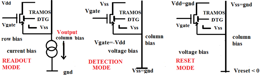
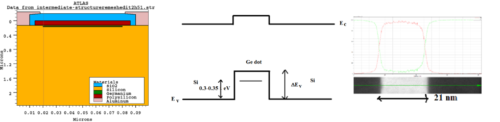
A pixel design has been proposed [25, 26]. The necessary simulations have been made to assess the functionality of the proposed device. The next step is to find out what is the best process to obtain the functionality and to reach some specifications. The principle of this pixel architecture (named DoTPiX) is the single n-channel MOS transistor, in which a buried quantum well gate performs two functions (Fig. 1): as a hole-collecting electrode and as a channel current modulation gate. Extensive simulations were made with this pixel architecture [25]; to assess its functionality, the buried quantum well gate is made with a Ge layer deposited on a silicon substrate. We are currently developing the basic structure with UHV/CVD techniques. The proposed structure is in its fabrication phase to obtain a test vehicle. The active layers where electron-hole pairs are created is of the order of m below the surface, enabling detection of minimum ionizing particles. The processed wafers (Fig. 2) should be compatible with advanced CMOS nodes including SOI (FDSOI) and nanowire devices. The surface roughness on the processed wafers (as measured by AFM) is low enough but should be slightly improved. We have established a working group with different institutes for this project.
5 Thin Film Detectors
Kim, Metcalfe, Sumant
Nanoscience technologies are developing new cutting edge materials and devices for a wide range of applications. HEP can take advantage of the many advances by looking toward thin film fabrication techniques to implement a new type of particle detector. Thin Film (TF) Detectors have the potential to be fully integrated, large area, low power, with low dead material, and low cost. The present goal is to investigate potential research paths using thin film technologies and to identify and characterize the performance benefits for future particle experiments.
A new detector technology is proposed based on thin films that is aimed at dramatically improving the precision of particle detectors by greatly reducing the mass of the detector [27]. Cleaner signatures of the particles from the primary collision will be obtained by reducing those particles’ interactions with dead material, which will improve reconstruction efficiencies and resolutions. Thin Film technologies could potentially replace the entire detector including all the services. If a thin film detector could be printed in large areas (square meters), it is estimated that the cost would be reduced to less than 1% of the current cost. If the nuclear interaction length can be decreased by a factor of 10, then the track reconstruction efficiencies would reach 99% and enable a host of new measurements and searches.
Thin Film technology presents one possible solution to achieve these performance milestones. TF transistors (TFT’s) were first conceived in the 1960’s by Paul Weimer [28]. By the 21st century, fabrication technologies had improved enough to make it competitive with existing technologies. TFT’s are the basis of technologies such as Liquid Crystal Display (LCD) screens, solar cells, and light emitting diodes. It is a rapidly growing technology area with a large market base and has corresponding investment in large scale fabrication and industrialization. Ultimately, the broader interest of these technologies enables HEP to leverage the investments in commercialization as well as the R & D into materials, tools, and techniques.
Some of the advantages of TF’s are optical transparency, mechanical flexibility, high spatial resolution, large area coverage, and low cost relative to traditional silicon-based semiconductor technology. TF technology uses crystalline growth techniques to layer materials. Monolithic sensors can be fabricated using layers of thin film materials for particle detection with layers for amplification electronics. The advantages of a detector made with this type of technology include single piece large area devices (on the order of a few square meters), high resolution (m), low cost (100 times less than that of Si-CMOS), low mass, and high curvature for a cylindrical, edgeless design [29]-[31].
Fabrication processes such as chemical bath deposition and close-space sublimation on a substrate material can produce thin films with a high degree of precision. Here, the crystalline structure is grown in layers, avoiding drilling and etching techniques standard in traditional silicon fabrication; consequently, TF processing is much less expensive.
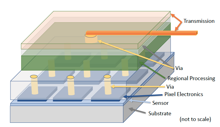
Thin film electronics can be vertically integrated with a thin film sensor if the fabrication techniques are compatible. This would allow vertical integration of sensor and pixel electronics. Further vertical integration using through-vias would enable signals to pass from one layer to the next, thus enabling several levels of electronic processing. Typical front-end ASIC functions could be integrated into the monolithic structure as well as higher-end processing to perform functions such as data aggregation and region-of-interest processing. Such processing would reduce the number of transmission lines integrated into a top layer and further reduce the material inside the detector volume. Figure 3 shows a potential vertical stack-up.
The transistor is the most basic unit that determines the power consumption in electronics. Complementary Metal Oxide Semiconductor (CMOS) is a low power technology and is the current mainstay for most of commercial electronics. There are, however, many types of transistor technologies that can outperform CMOS. Silicon Germanium (SiGe) Heterojunction Bipolar Transistors (HBT’s) are another class of transistor that typically boast faster speeds and lower power consumption [32]-[34]. Fin-Field Effect Transistors (FinFET’s) are being pursued as the next ultra-low power technology and are manufactured by companies such as IBM and Motorola. However, the most transformational transistor is the Thin Film Transistor (TFT), which is breaking records in terms of size and power. All of these technologies have the potential for reducing the power (and the copper in the transmission lines) over the current technologies.
Thin Film Detectors have the potential to replace a wide range of detector types from tracking to calorimetry. The present goals are to identify key areas of research within Thin Film technologies, quantify the key requirements from different types of experiments, and evaluate the potential physics impact.
6 Scintillating Quantum Dots in GaAs for Charged Particle Detection
Mahajan, Minns, Tokranov, Yakimov, Oktyabrsky, Gingu, Murat, Hedges
Future collider experiments will require particle detectors with timing resolution better than 10 ps; this is beyond the limits of existing technologies [35]. One possible avenue for innovation of charged-particle tracking relies on novel ultra-fast scintillating material utilizing semiconductor stopping media with embedded quantum dots [36, 37, 38].
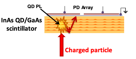
Fabrication of such a detector requires a scintillator with unique properties: very high light yield and a fast emission time. We have identified a candidate sensor material based on self-assembled InAs quantum dots (QDs) embedded into a GaAs matrix [36]. QDs are known to be excellent light emitters with close to 100% efficiency and emission times on the order of hundreds of picoseconds. To make a scintillator, however, one needs to embed QDs into a dense medium that is transparent to the QD photon emission. GaAs fulfills this requirement. An ideal sensor consists of two physically integrated systems:
-
1.
The scintillator: A charged particle travels through the InAs QD/GaAs scintillator and produces electron-hole pairs in the GaAs matrix ( pairs/MeV). The carriers are rapidly captured (within 2-5 ps) in the positively charged QDs due to high electron mobility of up to 8500 at room temperature. The infrared emission (1.1 eV photons) is red-shifted more than 300 mV from the bandgap of the GaAs matrix, resulting in low self-absorption () [37].
-
2.
The photodetectors: As the refraction index of GaAs is high (approximately 3.4), only of the emitted light exits the scintillator through one planar interface with air, and the rest gets reflected and travels inside the scintillator. Thus for efficient detection, the photodetector (PD) must be physically integrated with the scintillator. The proposed design has a matrix of InGaAs photodiodes fabricated directly on the surface of the scintillation matrix. The photodiode thickness is of the order of 1–2 microns, leading to efficient absorption of the QD emission. Photodiodes fully cover the scintillator area, resulting in uniform and efficient collection of the emitted light with close to unity fill factor.
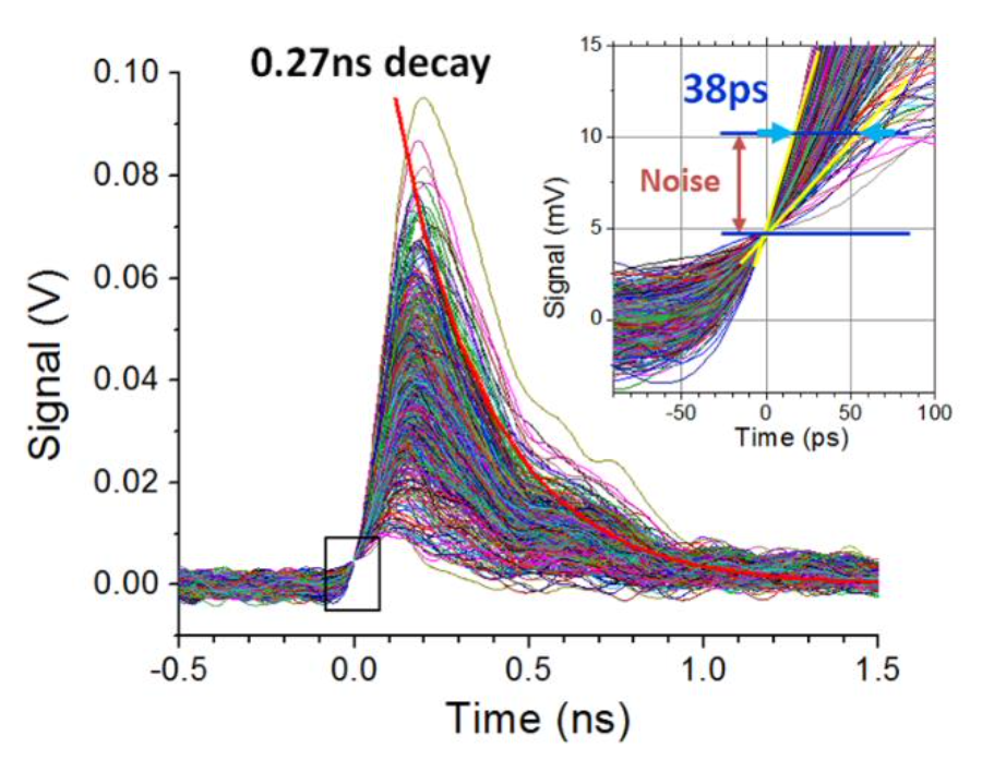
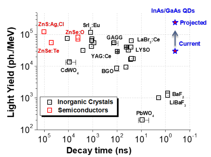
A schematic drawing showing this system is shown in Fig. 4. The first prototype detectors have been produced at SUNY Polytechnic Institute at Albany as thin wafers of micron thickness, each with a single integrated small area PD. The measurements of single-channel performance with particles have been published [37, 38, 39, 40]. Using -sources (5.5 MeV) and fast preamplifiers, we have measured a fast-decay constant of 270 ps and a 38 ps time resolution at room temperature without bias voltage applied to the PD. This performance, shown in Fig. 5, is currently limited by circuit noise and bandwidth. We measure detected electrons per 1 MeV of deposited energy with this system. Alternatively, a slower low-noise preamplifier demonstrated electrons/MeV of incident energy with longer ( ns) pulses. We expect performance to be near that of the theoretical optimum of electrons/MeV. A comparison of the performance of this detector with that of other scintillators is shown in Fig. 6. The demonstrated performance is, at the time of writing, the fastest and highest light yield of all known scintillators.
Significant exploratory research and development is required to accurately assess expected performance of these detectors in future high-energy physics applications. First, we must demonstrate detection performance with minimum ionizing particles, corresponding to expected signals of about 4000 electron-hole pairs in a single detector of m thickness. Given that the measurements with -particles are noise-limited, we also expect to encounter significant challenges developing a suitable electronics solution for optimal energy and timing performance for MIP detection. Furthermore, the radiation tolerance of this type of custom epitaxially-grown detector is not known, although the QD medium itself is among the most radiation hard semiconductor materials [41]. We will ultimately need to assess the performance of these detectors in the high-radiation environments expected in future high-energy physics experiments.
7 Conclusion
Five contemporary technologies are under development for applications at future high energy physics experiments. Collaborators interested in joining any of these efforts are welcome.
References
- [1] C. Da Vià, G. F. Dalla Betta, S. I. Parker, “Radiation sensors with three-dimensional electrodes,” CRC Press, Boca Raton, USA, ISBN, 9781498782234, January 2019.
- [2] B. Abbott et al. (The ATLAS IBL Collaboration), “Production and integration of the ATLAS Insertable B-Layer,” 2018 JINST 13 T05008.
- [3] F. Ravera, “The CT-PPS tracking system with 3D pixel detectors,” 2016 JINST 11, C11027.
- [4] D. Contardo et al., “Technical Proposal for the Phase-II Upgrade of the CMS Detector,” Tech. Rep. CERN-LHCC-2015-010. LHCC-P-008. CMS-TR-15-02, Geneva, June 2015.
- [5] G. F. Dalla Betta et al., “Development of a new generation of 3D pixel sensors for HL-LHC,” Nucl. Instr. and Meth. A 824 (2016) 386-387.
- [6] W. Riegler, “FCC-hh detector overview,” FCC week 2019, https://indico.cern.ch/event/727555/contributions/3461232.
- [7] Z. Drasal, “FCC-hh: Pile-up & PU Mitigation Studies,” FCC hadron detector meeting, July 2017, https://indico.cern.ch/event/650511/contributions/2651562/attachments/1488103/2312560/EffectivePU_ZDrasal.pdf.
- [8] G. Kramberger et al., “Timing performance of small cell 3D silicon detectors,” Nucl. Instr. and Meth. A 934 (2019) 26.
- [9] G.T. Forcolin et al., “Development of 3D trenched-electrode pixel sensors with improved timing performance,” 2019 JINST 14 C07011.
- [10] L. Anderlini et al., “Intrinsic time resolution of 3D-trench silicon pixels for charged particle detection,” 2020 JINST 15 P09029.
- [11] R. Mendicino et al., “3D Trenched-Electrode Sensors for Charged Particle Tracking and Timing,” Nucl. Instr. and Meth. A 927 (2019) 24-30.
- [12] G.F. Dalla Betta et al., “Feasibility Study of Charge Multiplication by Design in Thin Silicon 3D Sensors,” 2019 IEEE-NSS/MIC, Manchester, Session N-30.
- [13] S. Seidel et al., “Feasibility of Charge Multiplication by Design in Thin Silicon 3D Sensors,” CPAD 2019, Madison.
- [14] G.F. Dalla Betta et al., “Indication of Charge Multiplication by Design in Small-Pitch 3D Silicon Sensors,” in preparation.
- [15] J.-W. Tsung et al., “Signal and Noise of Diamond Pixel Detectors at High Radiation Fluences,” JINST 7, P09009 (2012).
- [16] S. M. Pimenov et al., “Femtosecond laser microstructuring in the bulk of diamond,” Diamond and Related Materials, 18 no. 2, 196 (2009).
- [17] B. Sun, P. S. Salter, and M. J. Booth, “High conductivity micro-wires in diamond following arbitrary paths,” Applied Physics Letters, 105, no. 23, 231105 (2014).
- [18] Y. Nagai, “Search for the Standard Model Higgs boson decaying into a b-quark pair at ATLAS,” CPPM Seminar, Oct. 20, 2014. https://indico.in2p3.fr/event/10662/attachments/1876/2381/CPPM_Seminar_nagai.pdf.
- [19] F. Pasquali, “Studies of b-jet identification without tracks with the ATLAS experiment at ATLAS at the LHC,” M.S. Thesis, University of Roma Sapienza, 2017. http://www.infn.it/thesis/PDF/getfile.php?filename=11752-Pasqualimagistrale.pdf.
- [20] T. Tanabe, “Tracking and Vertexing at Future (Linear) Colliders: Applications in Flavour Tagging,” January 19, 2017, IAS Program on High Energy Physics 2017, HKUST. http://ias.ust.hk/program/shared_doc/2017/201701hep/HEP_20170118_Tanabe.pdf.
- [21] M. Dentan et al., “Final acceptance of the DMILL technology stabilized at TEMIC/MHS,” Proc. of the 4th Workshop on Electronics for LHC Experiments, 1998.
- [22] S. Terzo, “Radiation hard silicon particle detectors for HL-LHC_RD50: status report,” Nucl. Instr. and Meth. A 845, 177-180 (2017); Proc. of the Vienna Conf. on Instrumentation 2016. http://www.sciencedirect.com/science/article/pii/S0168900216304120.
- [23] S.P. Griso, “Charged particles reconstruction in the ATLAS experiment,” LPNHE Seminar, Sept. 10, 2015. https://indico.in2p3.fr/event/11895/attachments/5890/7314/spagan_Tracking_LPNHE.pdf
- [24] T. Suehara, T. Tanabe, and S. Yamashita, “Improved Jet Clustering Algorithm with Vertex Information for Multibottom Final States,” Physics Procedia 37, 111-118 (2012); Proc. of the 2nd Int. Conf. on Technology and Instrumentation in Particle Physics (TIPP 2011). http://www.sciencedirect.com/science/article/pii/S1875389212016744.
- [25] N. T. Fourches, “Ultimate Pixel Based on a Single Transistor With Deep Trapping Gate,” IEEE Trans. on Electron Devices 64, pp. 1619-1623 (2017). https://doi.org/10.1109/TED.2017.2670681.
- [26] N.T. Fourches et al., “The TRAMOS pixel as a photo-detection device: Design, architecture and building blocks,” Nucl. Instr. and Meth. A 912, pp. 221-225 (2018), New Developments In Photodetection 2017. http://www.sciencedirect.com/science/article/pii/S0168900217312883.
- [27] J. Metcalfe et al., “Potential of Thin Films for use in Charged Particle Tracking Detectors,” arXiv:1411.1794 [physics.ins-det].
- [28] P.K. Weimer, “The TFT: A New Thin-Film Transistor,” Proc. of the IRE 50 (6) pp. 1462-1469 (1962).
- [29] B. Gnade, “Thin-Film Semiconductor Technology Applied to Large Area Radiation Detectors,” CIRMS Conference 2012. http://cirms.org/pdf/2012_conference_pdf/Tuesday Morning/cirms2012 Gnade.pdf.
- [30] I. Mejia et al., “Improved upper contacts PMMA on P3HT PTFTS using photolithographic processes,” Microelectronics Reliability 48, pp. 1795-1799 (2008).
- [31] R.A. Street, “Thin-Film Transistors,” Advanced Materials 21, pp. 2007-2022, Wiley (2009). https://onlinelibrary.wiley.com/doi/abs/10.1002/adma.200803211.
- [32] J.D. Cressler and G. Niu, Silicon-Germanium Heterojunction Bipolar Transistors, Artech House, Boston (2003).
- [33] J. Metcalfe et al., “Evaluation of the radiation tolerance of several generations of SiGe heterojunction bipolar transistors under radiation exposure,” Nucl. Instr. and Meth. A 579 (2) pp. 833-838 (2007).
- [34] J. Metcalfe et al., “Evaluation of the Radiation Tolerance of SiGe Heterojunction Bipolar Transistors Under 24-GeV Proton Exposure,” IEEE Trans. Nucl. Sci. 53 (6) pp. 3889-2893.
- [35] B. Fleming et al., “Report of the Office of Science Workshop on Basic Research Needs for HEP Detector Research and Development,” 2019.
- [36] S. Oktyabrsky et al., “Integrated semiconductor quantum dot scintillation detector: Ultimate limit for speed and light yield,” IEEE Trans. Nucl. Sci. 63 (2016) 656-663.
- [37] K. Dropiewski et al., “Optical properties of InAs quantum dots / GaAs waveguides for ultra-fast scintillators,” J. Luminescence 220 (2020) 116952.
- [38] K. Dropiewski et al., “Ultrafast Waveguiding Quantum Dot Scintillation Detector,” Nucl. Instr. and Meth. A 954 (2020) 161472.
- [39] A. Minns et al., “Parameters of fast and high-yield InAs/GaAs quantum dot semiconductor scintillator,” MRS Advances 6 (2020) 297-302.
- [40] T. Mahanjan et al., “Design and Performance Evaluation of InAs Quantum Dot Scintiallation Detector Properties with Monolithically Integrated Photodiode,” IEEE Sorma Proc. (2021), submitted.
- [41] S. Oktyabrsky et al., “Room-temperature defect tolerance of band-engineered InAs quantum dot heterostructures,” J. Appl. Phys. 98 (2005) 053512.