Resonant Soft X-Ray Scattering on LaPt2Si2
Abstract
X-ray absorption (XAS) and Resonant Inelastic X-ray Scattering (RIXS) spectra of LaPt2Si2 single crystal at the Si and La edges are presented. The data are interpreted in terms of density functional theory, showing that the Si spectra can be described in terms of Si and local partial density of states (LPDOS), and the La spectra are due to quasi-atomic local 4 excitations. Calculations show that Pt -LPDOS dominates the occupied states, and a sharp localized La state is found in the unoccupied states, in line with the observations.
1 Introduction
In the last decade, systems combining superconductivity (SC) and charge- and/or spin-density waves (CDW and/or SDW) order have attracted numerous attention. Materials like Fe-based pnictides [1], transition metal dichalcogenides [2] or cuprate superconductors [3] are three examples out of many. The interplay between CDW/SDW and SC remains unclear and subject of vigorous discussions.
Recently, the quasi-two-dimensional Pt-based rare earth intermetallic material LaPt2Si2 has attracted a lot of attention as it exhibits strong interplay between CDW and SC [4]. LaPt2Si2 crystallizes in a CaBe2Ge2-type tetragonal structure (space group P4/nmm, see Fig. 1(a)), having a close resemblance to the ThCr2Si2-type structure found in pnictide and heavy fermion systems. The striking difference between these two structures is that the former one lacks inversion symmetry in the crystal, resulting in two non-equivalent layers (Si1–Pt1–Si1) and (Si2–Pt2–Si2) arranged in alternating stacking separated by lanthanum atoms. This special feature in the crystal structure is reminiscent of noncentrosymmetric SC [4], where the lack of inversion symmetry results in nonuniform lattice potential, creating an asymmetric spin orbit coupling.
In polycrystalline samples, a first order transition was observed from high temperature tetragonal to low temperature orthorhombic phase, accompanied by a CDW transition around TCDW = 112 K followed by a SC transition at Tc = 1.22 K [4]. Below TSL = 10 K, superlattice reflections corresponding to (n/3, 0, 0), where n = 1 and 2 were observed, indicating that the unit cell of LaPt2Si2 is tripled in size along the [100] direction at low temperature [5]. Theoretical calculations show that the Fermi surface of LaPt2Si2 is of two-dimensional nature [6] and CDW and SC coexist in the (Si2–Pt2–Si2) layer. Recent investigations of LaPt2Si2 shows that the SC can be described in a single-gap -wave model with moderate coupling between electrons and phonons [7].
A CDW transition in this material was found some years ago [4], and multiple CDW transitions were recently observed [8], with a first CDW transition around 175 K at and and a second CDW transition around 100 K at and .
To get further insight into the interactions in this material, we have performed X-ray absorption (XAS) and resonant inelastic x-ray scattering (RIXS) experiments on a LaPt2Si2 single crystal at the Si and La edges.
The XAS spectrum shows sharp peaks at 97.1 eV, 101.47 eV and a dominating broad feature with maximum at 117.4 eV which can be assigned to excitation of atomic-like La states. RIXS spectra excited at these resonances show scattering to La final states, and we also observe X-ray Emission (XES) from the dynamically populated state to the ground state. The Si XES spectrum is stationary on the emission energy scale, and Partial Fluorescence Yield (PFY) is used to construct the Si XAS spectrum. Using density functional theory we show that the Si spectra can be described in terms of Si and local partial density of states (LPDOS). While Pt -LPDOS is predicted to dominate the occupied states, a sharp localized La state is found in the unoccupied states, in line with the observed quasi-atomic excitations.
2 Experiment
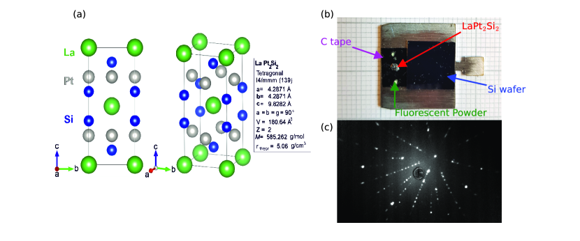
The single crystalline sample of LaPt2Si2 used in this study was synthesized using the Czochralski pulling method [4]. Crystallographic analysis shows that the LaPt2Si2 sample has P4/nmm space group with the crystallographic parameters given in Fig. 1(a). The VESTA software [9] was used to generate the crystal structure with crystallographic parameters from Gupta et al. [4]. The size of the sample used in this study was mm mm (1(b)). A diffraction pattern, obtained using the Laue backscattering method (Fig. 1(c)) shows that the sample is a single crystal.
XAS and RIXS spectra were measured at the SPECIES beamline [10, 11] at MAX IV Laboratory in Lund, Sweden. A silicon wafer was attached to the sample holder for energy calibration (Fig. 1(b)). Total Electron Yield (TEY) was measured via the drain current, both on the LaPt2Si2 sample, and the silicon reference. Normalization with respect to beamline flux was achieved via the gold-coated refocusing mirror drain current. The TEY measured from the silicon wafer was in good agreement with previous Si L2,3 XAS measurements [12].
XES spectra were measured using the Scientia model XES-350 spectrometer [13], which is a Rowland spectrometer equipped with three gratings and a micro-channel plate-based delay line detector [14]. For the measurements reported in this article, a grating with 3 m radius and 300 l/mm groove density was used. Energy calibration of the spectrometer relative to the monochromator was done using the elastic scattering of the incident photon beam, and the monochromator energy scale was set by the Si XAS reference [12]. The overall resolution was estimated from the full width at half maximum of the elastic scattering peak to be 270 meV at 108 eV incident photon energy. All RIXS measurements were carried out in the horizontal plane at 90∘ scattering angle, and the incident radiation was linearly polarized in the horizontal direction.
3 Theory
Density functional theory (DFT) calculations of the electronic structure of LaPt2Si2 have been performed with the Elk code [15] which implements the full-potential augmented plane waves and local orbitals method (FP-APW+lo) [16]. In tetragonal CaBe2Ce2 structure (space group , setting 2), the primitive cell of LaPt2Si2 contains 10 atoms. Calculations have been performed for this structure, using the lattice parameters reported by Gupta et al. [17]. We used the generalized gradient approximation (GGA) as parametrized in the PBE functional [18] for nonmagnetic, collinear spin-polarized, and noncollinear magnetic including spin-orbit coupling (SOC) calculations, using a maximum angular momentum , and a -centered k-point mesh of size .
4 Results and Discussion
In the Elk PBE collinear spin-polarized calculation, the electron band structures for majority and minority spins comes out as degenerate, from which we infer that LaPt2Si2 is a non-magnetic material. The electronic band structure in Elk PBE SOC calculation is shown in Fig. 2, with the associated total DOS, and projected partial DOS for La, Pt, and Si states shown in Fig. 3. At the La site a sharp La -LPDOS peak dominates the unoccupied states, and two sharp peaks in the La -LPDOS are found below -15 eV in the occupied states (Fig. 3a). It can be concluded that the La states are localized and do not contribute much to the band formation. The occupied states are dominated by Pt -LPDOS with a maximum around -4 eV (Fig. 3b) whereas -symmetry gives the largest contribution to the electronic structure at the Si sites (Fig. 3c), apart from a sharp peak in the Si -LPDOS at around -10 eV. By virtue of the dipole selection rules, X-ray spectra at the Si edges primarily probe the Si -LPDOS, and reflect the localized nature of the La -excitations at the La edges.
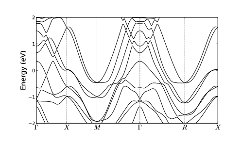

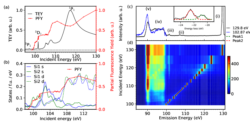
Figure 4(a) shows TEY obtained by the drain current from LaPt2Si2 as a function of incident photon energy. There are two sharp peaks at 97.1 eV and 101.47 eV, and a dominating broad feature with maximum at 117.4 eV, which can be assigned to excitation of atomic-like La states, including transitions to the bound LS-forbidden and states, and the giant resonance, respectively. Similar multiplet structures are typically observed in La compounds [19, 20, 21, 22], as a consequence of the atomic-like localized nature of the electrons.
Notably, the TEY spectrum does not capture the Si edge XAS of LaPt2Si2, expected to appear just below 100 eV. This observation demonstrates that the La absorption cross-section totally dominates over Si absorption. Instead, we observe TEY peaks between 104 and 108 eV (Fig. 4(a)) that match previous XAS spectra of SiO2 [12]. We attribute these peaks to an oxide layer formed on the surface of LaPt2Si2 crystal.
To address the Si absorption spectrum of LaPt2Si2 we first turn our attention to the XES map in Fig. 4(d). A complex pattern is observed, where the main intensity is stationary between 87 eV and 98 eV emission energy, primarily changing its integrated intensity with excitation energy. There is also an elastic peak for which the emission energy equals the excitation energy. A weaker structure disperses at constant 20-24 eV energy loss, and a sharp emission feature is observed at 101.46 eV constant emission energy. The latter is resonantly excited at incident photon energies around 120 eV. These features are denoted in the XES spectrum excited at 129.8 eV, shown in Fig. 4(c):
-
(i)
Elastic scattering, coinciding with the excitation energy.
-
(ii)
A constant-energy-loss feature which we assign to the scattering to 54 final states, reached over the 44 resonances. We tentatively assign the two peaks at 20.8 and 22.5 eV energy loss to final triplet states and the state, respectively, following the analysis of Suljoti et al. [22] and Miyahara et al. [23].
-
(iii)
A sharp peak at 101.46 eV emission energy assigned to emission from the dynamically excited state to the La ground state.
-
(iv)
A broad feature at constant emission energy, which we assign to principally Si emission, i.e., is associated with electrons from the valence band filling Si vacancies.
-
(v)
Si emission as in (iv), but as we see, the excitation energy dependence of the two features is different.
The red curve in Fig. 4(a and b) is the Partial Fluorescence Yield (PFY), constructed to emphasize Si excitations. As Si emission dominates features (iv) and (v), intensity in the corresponding 85-98 eV emission energy range was integrated to construct the PFY spectrum, while intensity from the dispersing La feature (ii), which contributes in the 110-120 eV excitation-energy range (Fig. 4c inset) was subtracted.
The Si edge shown in the PFY spectrum is found at 99.5 eV, and there is a sharp second intensity increase at 101.4 eV, almost coinciding with the La resonance, and another intensity increase around 107 eV.
There is only a faint structure in PFY at the sharp SiO2 excitations around 104 eV which can be attributed to the surface oxide. For oxidized silicon surfaces, a similar observation has been made for oxide layers of around 7 nm thickness [12]. While the fluorescence yield sampling depth in silicon is estimated to be 70 nm, [12], it is similar in this compound except for the region of the La giant resonance where the sampling depth is more than three-fold reduced [24]. We can therefore estimate the oxide layer also for LaPt2Si2 to be in the 7 nm range.
While the Si edge PFY spectrum gives information about the bulk material below the surface oxide layer, it does not directly represent the cross-section for Si excitations. The PFY minimum at 117.3 eV coincides with the maximum of the La giant resonance. At these energies, La absorption dominates the XAS spectrum of LaPt2Si2. As this process competes with Si absorption, and since La holes do not emit appreciably in the chosen emission energy range, the observed broad dip in the PFY is expected. The mechanism is the same as exploited in the inverse partial yield method [25].
In Fig. 4(b) we compare the the PFY with the Si and LPDOS, separated into contributions from the Si1 and Si2 sites (see Fig. 1 for notation). Significant differences between the two sites are predicted, e.g., the absorption close to the edge is primarily of Si2 character. The PFY increase around 101.4 eV coincides with increasing Si1 -LPDOS, while the 107 eV increase matches the increase in Si -LPDOS. We assign the main PFY features accordingly.
4.1 Elastic Peak (i)
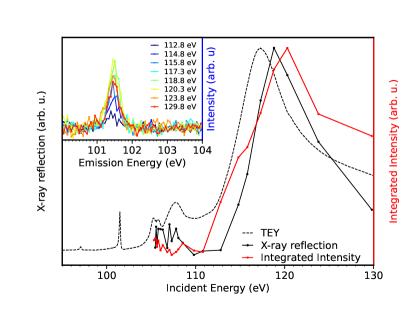
In general, the elastic peak (i) can have contributions from both diffuse reflection and the resonant absorption-emission process. Emission from the giant resonance in lanthanum compounds in low-energy electron excited spectra seemingly coincides with the absorption [20], demonstrating that a captured electron is sufficiently localized to recombine with the hole. The giant resonance is also observed in reflection measurements [19]. Considering the complex index of refraction, , it has been noted that if the normal-incidence reflectivity varies as the square of the absorption cross section. While this is often the case in this energy range [26], this approximation does not hold at the giant resonance, for which tabulated optical constants [24] imply a high-energy shift of the reflectivity peak relative to the peak in the absorption cross section. This predicted shift is consistent with the observed difference in peak positions when comparing the excitation-energy dependence of the elastic peak intensity and the TEY spectrum (Fig. 5). While the curves show similarities, there are also significant differences, the TEY spectrum peaks at 117.5 eV, and the maximum in the elastic-peak intensity is around 119 eV. We therefore conclude that the elastic peak is dominated by diffuse reflection in the region of the giant resonance.
4.2 Dispersing Feature (ii)
The dispersing double-peak feature (ii), assigned to lanthanum scattering is shown in the inset of Fig. 4(c). The two peaks are fitted with Gaussians at 22.5 and 20.7 eV energy loss, with full width at half maximum (FWHM) of 1.1 eV and 1.0 eV, respectively. The energy positions are close to the corresponding transitions in ionic lanthanum compounds [21, 22], facilitating the assignment of the high-energy loss peak to the final state, and the low-energy loss peak to “spin-flip” states. The intensity ratio of the two peaks also coincides with the earlier studies, again demonstrating the atomic-like nature of the scattering at the La sites.
In the ionic compounds the final states are situated in the band gap, whereas in the present case they are found in the conduction band far above the ionization thresholds. Therefore, delocalization via interaction with the continuum is allowed, just like in the case of the giant resonance. We tentatively attribute the additional width to tunneling of the excited electron through a barrier, analogously to the case of the singlet state. With this interpretation the increased width implies a reduction of the lifetime of the final states to less than 1 fs due to this additional decay channel.
4.3 Emission at 101.46 eV (iii)
Within the measurement accuracy, the energy of the stationary feature (iii) (Fig. 4c), 101.46 () eV, matches the energy of the La resonance (101.47 eV). Therefore, it can be assigned to transitions from this state to the lanthanum ground state.
The mechanism for off-resonance population of states in lanthanum compounds has been addressed earlier [19, 20], and the associated population of La states have been termed “shake-down” [27].
The transition energy is below the binding energies [28], i.e., the hole pulls down the orbitals below threshold. Consequently, the holes are screened as an electron from the valence band fills the level, forming states, where denotes a hole in the valence band. If this hole in the valence band delocalizes prior to the decay, the transition mirrors the resonance.
In Fig. 5 we see that the intensity of the emission to a large extent follows the absorption cross section, which is in line with the notion that the cross section in the range is totally dominated by La excitations. However we find the maximum in the yield slightly above 120 eV, and more than 2.5 eV above the absorption maximum. This shift can be understood by considering the localization of the initially excited electron. It is well-known that the probability that this electron tunnels through the potential barrier prior to the core hole decay increases with excitation energy over the giant resonance [29, 21]. As long as the initial electron remains local it contributes to the screening of the hole and hampers alternative screening mechanisms. Only when it delocalizes the screening from the valence band to the triplet coupled states becomes important. In this way the yield in this range reflects a dynamical process where the excitation is followed by tunneling of the electron, and subsequent screening from the valence band to triplet coupled states. In this sense the yield monitors the cross section for excitation of unscreened La holes.
4.4 Si emission (iv and v)
4.4.1 LPDOS and XES
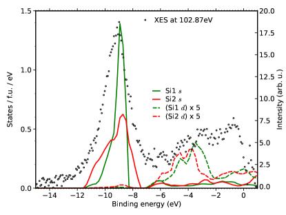
The emission shown in Fig. 6, excited at 102.87 eV, is shifted to the binding energy scale by subtracting 98.97 eV, as determined by the apparent valence band edge. From the edge, the spectrum shows a plateau down to around -6 eV, followed by a peak with a maximum around -9.5 eV. The experimental results are compared to the Si and -LPDOS (Fig. 6) at the two crystallographic sites, Si1 and Si2, as denoted in Fig. 1. The low-energy peak can be unambiguously assigned to transitions from states of Si character as the Si -LPDOS dominates in this region. In the predicted LPDOS there is a marked difference between the two sites. Whereas the Si1 -LPDOS has a rather sharp peak at -9 eV, the Si2 -LPDOS is more smeared out. Due to the broadening mechanisms, especially the lifetime broadening of final-hole states far from the Fermi level [30] we do not expect this difference to be observable. The FWHM of the experimental peak is around 2 eV, while a Lorentzian broadening of 1 eV is applied to the theoretical LPDOS.
The Si -LPDOS is not sufficient to capture the plateau in XES spectrum between the valence band edge and -6 eV, as density relative to the -9 eV peak is small in this region. Assuming that the Si -LPDOS gives a factor of 5 larger contribution to the XES intensity than the Si -LPDOS, the intensity in this region can be partly explained (Fig. 6). Since the Si radial overlap typically is larger than the overlap, Si -states are expected to contribute more to Si emission than Si -states [31], but a factor of 5 is unusually large. We also note that upscaled Si -LPDOS introduces spectral structure that is not observed in the experimental spectrum.
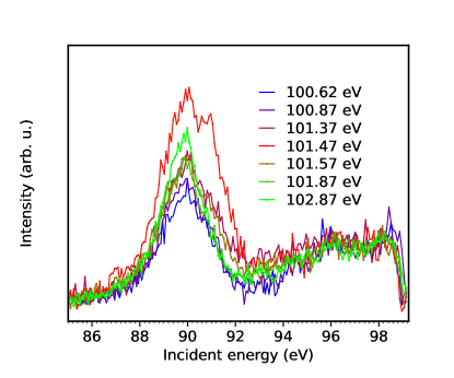
4.4.2 Excitation-Energy Dependence
The spectral changes as the excitation energy varies across the La absorption peak are shown in Fig. 7. We find that the spectra normalized at 98 eV, show a steep resonant behavior where the intensity of the peak at 90 eV (-9 eV peak in Fig. 6) increases, and a pronounced shoulder develops around 91 eV, and attains maximum intensity when the incident energy is tuned to the La resonance.
It is tempting to interpret this behavior as due to transitions involving La intermediate state. In this state the electron is localized at the lanthanum site, and in principle a valence electron can fill the core hole, to create a final state with a vacancy in the valence band and an excited electron. The sharp peak in the unoccupied La LPDOS of the electronic ground state (Fig. 3) suggests that the electron is localized also in the final state. According to dipole selection rules transitions from the valence band to a La hole should be from state with La or character. However, the theory does not show appreciable LPDOS of these local symmetries (Fig. 3), and it lacks steep structures that could directly account for the observations.
Tentatively, we still associate the resonant behavior to transitions to the La 4 level from the valence band. With the excitation energy at 101.47 eV, and the emission energy of the resonant shoulder is 91 eV, the energy loss is 10.5 eV, suggesting that the corresponding hole is in the band that is dominated by Si states. Especially, the Si1 site, which is in closest proximity to the La atoms has a sharp peak at the corresponding energy (fig. 3). The observations are consistent with a ”cross transition” where the final state has an electron in the band dominated by La -LPDOS and a vacancy in the band dominated by Si1 -LPDOS, and we speculate that excitonic effects, and possibly interference between close-lying core-hole states may enable pathways to such final states.
Finally we note that there is a slight spectral change, when comparing data taken below and above the resonance. They are consistent with selective excitation of the two silicon sites, which show large variation at the cross section at these excitation energies (Fig. 4b).
5 Conclusions
XAS and RIXS measurements at Si and La edges of LaPt2Si2 are presented, and interpreted in terms of DFT calculations. Atomic-like local La excitations are found in the absorption spectrum, the forbidden , and excitation as well as the giant resonance. Decay to final states are observed, and also the decay of the dynamically populated state to the electronic ground state. Observations suggest that resonantly excited states also decay via valence band emission. The Si XAS spectra are measured via PFY, and the XES spectra are independent of the excitation energy over most of the energy range. The spectra are assigned using the theoretical LPDOS of Si and character at both crystallographic Si sites.
Since this system is similar to 122 Fe based superconductors and shows CDW formation at lower temperatures, we should expect to see a variation in electronic interaction between La and Si atoms as a function of temperature, and an accompanying variation in the Si and La spectra. With site selectivity the question to what extent the CDW primarily is formed in the Si1-Pt2-Si1 or Pt1-Si2-Pt1 layers can be addressed.
A more detailed study will follow, including a systematic investigation of the temperature dependence across the CDW transition, and the dependence on crystal orientation.
References
References
- [1] M. D. Lumsden and A. D. Christianson. Magnetism in fe-based superconductors. Journal of Physics: Condensed Matter, 22(20):203203, apr 2010.
- [2] Sajedeh Manzeli, Dmitry Ovchinnikov, Diego Pasquier, Oleg V. Yazyev, and Andrãs Kis. 2D transition metal dichalcogenides. Nature Reviews Materials, 2(8):17033, aug 2017.
- [3] B. Keimer, S. A. Kivelson, M. R. Norman, S. Uchida, and J. Zaanen. From quantum matter to high-temperature superconductivity in copper oxides. Nature, 518(7538):179–186, 2015.
- [4] Ritu Gupta, S. K. Dhar, A. Thamizhavel, K. P. Rajeev, and Z. Hossain. Superconducting and charge density wave transition in single crystalline LaPt 2 Si 2. Journal of Physics: Condensed Matter, 29(25):255601, jun 2017.
- [5] Yutaro Nagano, Nobutaka Araoka, Akihiro Mitsuda, Hideki Yayama, Hirofumi Wada, Masaki Ichihara, Masahiko Isobe, and Yutaka Ueda. Charge density wave and superconductivity of RPt2Si2 (R = Y, La, Nd, and Lu). Journal of the Physical Society of Japan, 82(6):18–22, 2013.
- [6] Sooran Kim, Kyoo Kim, and B. I. Min. The mechanism of charge density wave in Pt-based layered superconductors: SrPt2As2 and LaPt2Si 2. Scientific Reports, 5(1):15052, dec 2015.
- [7] Z. Y. Nie, L. C. Yin, A. Thamizhavel, A. Wang, B. Shen, L. Q. Che, F. Du, Z. Hossain, M. Smidman, X. Lu, and H. Q. Yuan. Nodeless superconductivity in the charge density wave superconductor . Phys. Rev. B, 103:014515, Jan 2021.
- [8] M. Falkowski, P. DoleŽal, E. Duverger-Nédellec, L. M. Chamoreau, J. Forté, A. V. Andreev, and L. Havela. Multiple charge density wave states and magnetism in NdPt2Si2 against the background of its nonmagnetic analog LaPt2Si2. Physical Review B, 101(17):174110, may 2020.
- [9] Koichi Momma and Fujio Izumi. VESTA3 for three-dimensional visualization of crystal, volumetric and morphology data. Journal of Applied Crystallography, 44(6):1272–1276, Dec 2011.
- [10] Samuli Urpelainen, Conny Såthe, Walan Grizolli, Marcus Agåker, Ashley R. Head, Margit Andersson, Shih Wen Huang, Brian N. Jensen, Erik Wallén, Hamed Tarawneh, Rami Sankari, Ralf Nyholm, Mirjam Lindberg, Peter Sjöblom, Niclas Johansson, Benjamin N. Reinecke, M. Alif Arman, Lindsay R. Merte, Jan Knudsen, Joachim Schnadt, Jesper N. Andersen, and Franz Hennies. The SPECIES beamline at the MAX IV Laboratory: A facility for soft X-ray RIXS and APXPS. Journal of Synchrotron Radiation, 24(1):344–353, 2017.
- [11] Esko Kokkonen, Felipe Lopes da Silva, Mikko-Heikki Mikkelã, Niclas Johansson, Shih-Wen Huang, Jenn-Min Lee, Margit Andersson, Antonio Bartalesi, Benjamin N. Reinecke, Karsten Handrup, Hamed Tarawneh, Rami Sankari, Jan Knudsen, Joachim Schnadt, Conny Såthe, and Samuli Urpelainen. Upgrade of the SPECIES beamline at the MAX IV Laboratory. Journal of Synchrotron Radiation, 28(2):588–601, Mar 2021.
- [12] M. Kasrai, W. N. Lennard, R. W. Brunner, G. M. Bancroft, J. A. Bardwell, and K. H. Tan. Sampling depth of total electron and fluorescence measurements in Si L- and K-edge absorption spectroscopy. Applied Surface Science, 99(4):303–312, 1996.
- [13] Joseph Nordgren and Jinghua Guo. Instrumentation for soft x-ray emission spectroscopy. Journal of Electron Spectroscopy and Related Phenomena, 110-111:1–13, 2000. Soft X Ray Emission Spectroscopy.
- [14] A. Oelsner, O. Schmidt, M. Schicketanz, M. Klais, G. Schönhense, V. Mergel, O. Jagutzki, and H. Schmidt-Böcking. Microspectroscopy and imaging using a delay line detector in time-of-flight photoemission microscopy. Review of Scientific Instruments, 72(10):3968–3974, 2001.
- [15] The Elk FP-LAPW code. Available under GNU General Public License. http://elk.sourceforge.net/.
- [16] David J Singh and Lars. Nordström. Planewaves, Pseudopotentials and the LAPW Method. Springer Science+Business Media, Inc., Boston, MA, second edition, 2006.
- [17] Ritu Gupta, U. B. Paramanik, S. Ramakrishnan, K. P. Rajeev, and Z. Hossain. Coexistence of superconductivity and a charge density wave in LaPt2Si2. Journal of Physics: Condensed Matter, 28(19):195702, may 2016.
- [18] J.P. Perdew, Kieron Burke, and Matthias Ernzerhof. Generalized gradient approximation made simple. Physical review letters, 77(18):3865–3868, oct 1996.
- [19] D. R. Mueller, C. W. Clark, D. L. Ederer, J. J. Jia, W. L. O’Brien, Q. Y. Dong, and T. A. Callcott. Charge-transfer-induced multiplet structure in the N4,5 O2,3 soft-x-ray emission spectrum of lanthanum. Physical Review A, 52(6):4457–4461, dec 1995.
- [20] Kouichi Ichikawa, Atsushi Nisawa, and Kenjiro Tsutsumi. Radiative decay of 4d94fn+1 excited states in LaB6 and CeB6. Physical Review B, 34(10):6690–6694, 1986.
- [21] J. E. Rubensson, J. Lüning, S. Eisebitt, and W. Eberhardt. It’s always a one-step process. Applied Physics A: Materials Science and Processing, 65(2):91–96, 1997.
- [22] E. Suljoti, F. M. F. de Groot, M. Nagasono, P. Glatzel, F. Hennies, M. Deppe, A. Pietzsch, B. Sonntag, A. Föhlisch, and W. Wurth. Spin-orbit mediated interference in the radiative and nonradiative channels of the la core resonances. Phys. Rev. Lett., 103:137401, Sep 2009.
- [23] Tsuneaki Miyahara, Hiroo Kato, Takaaki Hanyu, Hiroyoshi Ishii, Mihiro Yanagihara, Toru Kamada, Kenzo Naito, and Shoji Suzuki. The 4d Photoabsorption Spectra of La, LaF3, Ba and BaF2: Dependence on the Chemical and Structural Environment. Journal of the Physical Society of Japan, 55(1):408–413, jan 1986.
- [24] B.L. Henke, E.M. Gullikson, and J.C. Davis. X-ray interactions: Photoabsorption, scattering, transmission, and reflection at e = 50-30,000 ev, z = 1-92. Atomic Data and Nuclear Data Tables, 54(2):181–342, 1993.
- [25] A. J. Achkar, T. Z. Regier, H. Wadati, Y.-J. Kim, H. Zhang, and D. G. Hawthorn. Bulk sensitive x-ray absorption spectroscopy free of self-absorption effects. Phys. Rev. B, 83:081106, Feb 2011.
- [26] W.L. O’Brien, J. Jia, Q-Y. Dong, T.A. Callcott, J.-E. Rubensson, D.L. Mueller, and D.L. Ederer. Resonant absorption and emission from localized core-hole states in Al2O3 and SiO2. Nuclear Instruments and Methods in Physics Research Section B: Beam Interactions with Materials and Atoms, 56-57(PART 1):320–323, may 1991.
- [27] Makoto Okusawa, Kouichi Ichikawa, Osamu Aita, and Kenjiro Tsutsumi. Hole-induced shakedown process in the M4,5 fluorescent emission spectrum of lanthanum. Physical Review B, 35(2):478–481, 1987.
- [28] S. P. Kowalczyk, N. Edelstein, F. R. McFeely, L. Ley, and D. A. Shirley. X-ray photoemission spectra of the 4d levels in rare-earth metals. Chemical Physics Letters, 29(4):491–495, 1974.
- [29] O P Sairanen, S. Aksela, and A. Kivimaki. Resonance Auger and autoionization processes in solid lanthanum after 4d to 4f resonant excitation by synchrotron radiation. Journal of Physics: Condensed Matter, 3(44):8707–8714, nov 1991.
- [30] J. A. Knapp, F. J. Himpsel, and D. E. Eastman. Experimental energy band dispersions and lifetimes for valence and conduction bands of copper using angle-resolved photoemission. Phys. Rev. B, 19:4952–4964, May 1979.
- [31] H. Yorikawa. X-ray emission spectra of 3c-sic studied by tight-binding model including d orbitals. Journal of Electron Spectroscopy and Related Phenomena, 184(7):379–383, 2011.