Broadband single-mode planar waveguides in monolithic 4H-SiC
Abstract
Color-center defects in silicon carbide promise opto-electronic quantum applications in several fields, such as computing, sensing and communication. In order to scale down and combine these functionalities with the existing silicon device platforms, it is crucial to consider SiC integrated optics. In recent years many examples of SiC photonic platforms have been shown, like photonic crystal cavities, film-on-insulator waveguides and micro-ring resonators. However, all these examples rely on separating thin films of SiC from substrate wafers. This introduces significant surface roughness, strain and defects in the material, which greatly affects the homogeneity of the optical properties of color centers. Here we present and test a method for fabricating monolithic single-crystal integrated-photonic devices in SiC: tuning optical properties via charge carrier concentration. We fabricated monolithic SiC n-i-n and p-i-n junctions where the intrinsic layer acts as waveguide core, and demonstrate the waveguide functionality for these samples. The propagation losses are below 14 dB/cm. These waveguide types allow for addressing color-centers over a broad wavelength range with low strain-induced inhomogeneity of the optical-transition frequencies. Furthermore, we expect that our findings open the road to fabricating waveguides and devices based on p-i-n junctions, which will allow for integrated electrostatic and radio frequency (RF) control together with high-intensity optical control of defects in silicon carbide.
In recent years silicon carbide has gained interest for quantum technology applications in fields like communication Koehl et al. (2011); Zwier et al. (2015); Widmann et al. (2019); Majety et al. (2021) and (bio)sensing Saddow et al. (2011); Simin et al. (2015). It was found that color centers in SiC have favorable properties, such as long-lived spin states and possibilities for operation at telecom wavelengths Bosma et al. (2018); Spindlberger et al. (2019); Wolfowicz et al. (2020). For scaling down potential opto-electronic quantum applications, integrated photonics are paramount. In silicon carbide it would be simple to combine such architectures with existing silicon and silicon-carbide device platforms.
Though many examples exist of amorphous SiC waveguides Pandraud et al. (2007); Zheng et al. (2019); Zhang et al. (2020), a high-quality single-crystal material is required in order to get reliable spin-active color centers with predetermined properties Bosma et al. (2018). Crystalline waveguides and photonic devices have been fabricated for various SiC polytypes such as photonic crystal cavities with arrays of cylindrical holes in 3C-SiC Calusine, Politi, and Awschalom (2014), 4H-SiC film-on-insulator waveguides Lukin et al. (2020) and micro-ring resonators Martini and Politi (2017); Zheng et al. (2019).
Inspired by recent studies on color-center defects in silicon carbide, showing combined electrical and optical control of color-center defects in silicon carbide for quantum technologies in p-i-n junctions Falk et al. (2014); Widmann et al. (2018, 2019); Anderson et al. (2019), we report here on developing another method for fabricating monolithic SiC waveguides: engineering a lower value for the index of refraction for cladding layers via a high concentration of free charge carriers Hunsperger (2009). The main reason for this choice is that for technologies involving color centers, especially ensemble based, high material purity and low strain-induced inhomogeneity are vital. This grade of material quality, however, can only be achieved when growing 4H-SiC device layers on substrates of the same material. The layers are difficult to separate without loss of homogeneity Zheng et al. (2019).
In this work we show how junctions from layers with alternating doping concentration can be engineered into single-mode optical waveguides. We fabricated n-i-n and p-i-n junction planar structures in 4H-SiC as a proof of concept. These devices can be engineered to confine any preferred number of waveguide modes. Notably, the number of allowed modes, as well as their field distribution, is independent of wavelength for a very wide range, as long as the associated optical frequency is above the plasma frequency. We demonstrate these broadband properties (for 700 to 1290 nm light) of the n-i-n single-mode waveguides with a core thickness of m and cladding doping concentration up to , and we present consistent results for p-i-n waveguides. Our findings indicate that it is possible to have electrostatic and RF control for SiC color centers in the core layer of n-i-n and p-i-n structures by the (AC) Stark effect Falk et al. (2014); de las Casas et al. (2017), while having high-intensity optical control via the waveguide at the same time. For SiC mature semiconductor processing techniques are available, such that device structures with one-dimensional photonic channels can be developed.
I Tuning the refractive index via carrier-concentration
According to the Drude model, a plasma of free charge carriers reduces the refractive index Bond et al. (1963); Bennett, Soref, and Del Alamo (1990); Fox (2010) for optical frequencies above the plasma frequency. They screen a material from the optical electric field, thereby lowering the net polarization and thus the index of refraction . As explained in Appendix A.1, the influence of free carriers on the refractive index leads to a shift
| (1) |
where is the concentration of free charge carriers with effective mass , is the elementary charge, is the vacuum permittivity, the speed of light in vacuum, the refractive index of the undoped host material and the vacuum wavelength for which we evaluate the refractive index. Increasing the free-carrier concentration will thus decrease the refractive index for 4H-SiC Yoshida, Hijikata, and Yaguchi (2012); Sedighi et al. (2014). This should allow for total internal reflection at shallow reflection angles.
II Sample materials
The n-i-n planar waveguide samples used in this research are grown on an n++ 4H-SiC substrate (). Using epitaxial chemical vapor deposition growth in which the nitrogen concentration for n-type doping could be controlled, first a m layer of minimally doped () SiC is grown as the waveguide core. Next, a highly doped layer () of m is deposited on top to serve as cladding. The material was then cleaved along the direction and its orthogonal to yield several samples of 3.2 and 6.9 mm length with very smooth facets.
The p-i-n planar waveguides were produced in a similar way, where aluminum is used for the highly p-doped layer. A minimally doped layer () of m thickness is deposited on top of a highly n-doped 4H-SiC substrate (), after which a layer with a highly p-doped layer () of m thickness is deposited on top of the intrinsic layer. Also this sample was cleaved along the direction and its orthogonal, yielding samples of 2.8 and 5 mm length. Facets with rough edges were polished to improve the surface quality.
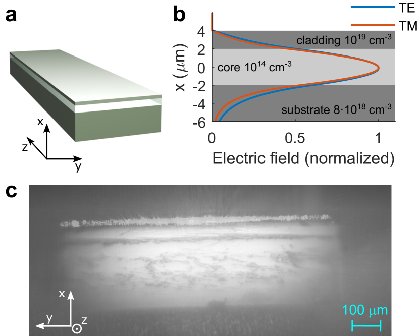
According to Eq. (1) the step in index of refraction between the core and cladding is for 800 nm TE polarized light, where it is assumed that each n-dopant donates one electron to the conduction band or donates one hole to the valence band in the case of the doped cladding layer. With this knowledge we can predict the electric field distribution for the optical modes. The expected field distributions for TE and TM modes in the n-i-n junction are shown in Fig. 1b Hammer (2020). Due to the relatively low contrast in refractive index between the core and the cladding and substrate layer, wee see that a significant fraction of the electric field of the mode is outside the core layer. Interestingly, the shape of these modes is wavelength independent due to two competing effects. For increasing wavelengths, the reduction of round-trip phase for the optical field bouncing between the substrate and cladding layers is compensated by the increase in the range of total internal reflection angles Hunsperger (2009). This is discussed in detail in Appendix A.2.
Finally, we note that both the shallow n and p-dopants emit with near-bandgap energies, and mostly behave as contributors to the charge carrier plasma. Therefore, they have little optical interactions in the near-infrared spectral window of the color centers.
III Mode matching
To investigate the waveguide functionality, we evaluate the transmission and confinement of a single-mode laser beam through the sample. For this purpose we used a 700-1000 nm tunable CW Ti:Sapphire laser, and tunable diode lasers for use around 1100 and 1300 nm. For initial testing we focused an 800 nm beam to a diameter of m and aligned it to the waveguide layer using a stepper-motor controlled six-axis stage. Figure 1c shows a camera image of the end facet of a sample for optimal mode coupling at the input side (related video data is available online as Supplementary Material). Along the top edge, a bright transmission band is visible, confirming the confinement of the optical field in the n-i-n core layer.
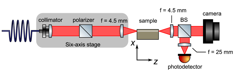
We further study the mode matching and coupling efficiency by measuring the transmission versus focusing-lens position (for the focal point near the input facet). Figure 2 shows the experimental setup. A single-mode fiber attached to a six-axis stage feeds a wavelength-tunable laser to the setup. On the stage the laser beam with 1.2 mm diameter is polarized and focused by an aspheric lens with mm focal length. By scanning the position of the stage, the focal point of the laser can be scanned along the input facet of sample. The transmission is captured by a photodetector and a camera focused at the end facet of the sample. We repeat these scans for several wavelengths in order to study the wavelength dependence of the mode matching.
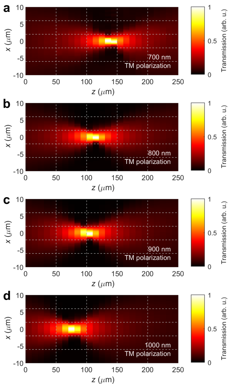
Figure 3 presents the results for scanning along the optical axis () and sample layers () of the n-i-n junction for TE polarization, i.e. polarization along the sample plane. Similar results for TM polarization, as well as results for longer wavelengths (up to 1290 nm), are presented in Appendix A.3. The results show a clear maximum in the amount of transmitted light, which reduces symmetrically according to a reduction in mode matching between the focus in a single-mode Gaussian beam and the waveguide mode, when shifting the lens in the and direction. This confirms that we couple in maximally when the input facet is fully in focus. We will further characterize this mode matching by determining the peak height and peak width (as full-width at half maximum, FWHM) of Gaussian fits of traces along the -axis for data as in Fig. 3. At the narrowest, the FWHM is m, independent of wavelength. Note that the shift of the optimal coupling point along with wavelength matches with the wavelength dependence for the focal length of the used aspheric lens, as specified by the supplier Thorlabs (2020).
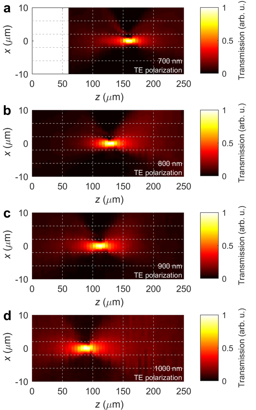
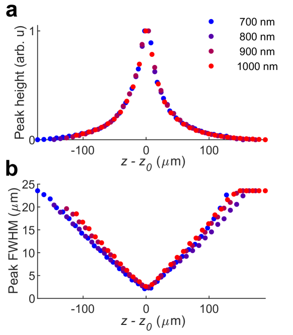
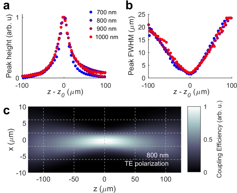
Figure 4a,b present the mode-matching peak heights and FWHM for the four wavelengths used for measuring Fig. 3a-d. Figure 4a shows the value of the transmission maximum for each position along , relative to the overall transmission maximum at . Figure 4b shows the FWHM. Both the peak width and height are unaffected by wavelength changes in this range, confirming that the mode distribution within the waveguide core is independent of wavelength. Figure 4c shows a theoretical prediction of the coupling efficiency for various beam positions at 800 nm. The coupling-efficiency profile matches well with the transmission profile from Fig. 3b. This estimate was obtained by solving the overlap integral for optical powers Chang et al. (2017)
| (2) |
with the complex electric field of the laser beam and the electric field for the waveguide mode. These electric-field terms were determined based on the experimental-setup parameters and the predicted waveguide mode from Fig. 1b, respectively.
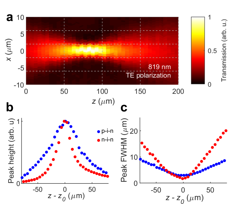
We repeated the mode-matching measurement of the n-i-n junction for the p-i-n junction with light and TE polarization. The results are displayed in Fig. 5, showing similar behavior to both the experimental results of the n-i-n junction and the theoretical prediction in Fig. 4c. Directly comparing results for the p-i-n junction to the results of the n-i-n junction (Fig. 5b,c) shows that the mode-matching peak height and FWHM of the p-i-n junction depend less strongly on the -position of the focusing-lens than for the n-i-n junction. This is because of the increased height of the mode (along ) in the p-i-n material. This results from the fact that the value is lower for this sample, due to a lower charge carrier concentration and the higher effective mass of holes compared to electrons Son et al. (2000). Consequently, the overlap integral in Eq. (2) is less sensitive to a change in diameter of the field. This is also visible from the minimum peak FWHM, which is m for the p-i-n junction (Fig. 5c).
We obtained a rough indication for the propagation losses by comparing the transmission at optimal coupling for n-i-n and p-i-n samples of varied lengths ( and mm, and and mm respectively). We found that for both TE and TM polarization the propagation losses must be below in the nm wavelength range. We expect that a part of these losses is due to free-carrier (intraband) absorption in the highly doped layers around the core, where around of the electric field is present. Other mechanisms are surface scattering and losses due to imperfections in the setup, such incomplete collection of the light due to beam divergence inside the planar waveguide. To what extent each of these mechanisms contribute will be tested better in future work where these materials are processed into elongated one-dimensional waveguides.
IV Conclusions
In this research we have studied the feasibility of using strong doping of 4H-SiC for realizing cladding layers around a (near) intrinsic 4H-SiC optical waveguide core. This provides a path to waveguides in single-crystal high-purity 4H-SiC material. We fabricated monolithic planar waveguides that allow for broadband single-mode operation. We found as a rough upper bound for the propagation losses , which is low enough for on-chip applications. At a typical on-chip length scale of m less than of the optical intensity will then be dissipated. As follow-up we propose to process and test actual one-dimensional photonic channels from these materials, and to engineer n-i-n or p-i-n junction waveguide with color-center defects in the waveguide core (such as divacancies or vanadium impurities Koehl et al. (2011); Zwier et al. (2015); Widmann et al. (2019); Saddow et al. (2011); Simin et al. (2015); Bosma et al. (2018); Spindlberger et al. (2019); Wolfowicz et al. (2020)). This can demonstrate the true potential of these devices for quantum technologies with on-chip high-intensity optical driving of color centers.
V Supplementary Material
See the supplementary material for video data that supports Fig. 1c for different -positions of the focusing-lens.
Acknowledgements.
We thank R. H. van der Velde, F. Šimić, R. J. M. Julius, O. V. Zwier and D. O’Shea for discussions and experimental contributions. We thank M. de Roosz, J. G. Holstein, T. J. Schouten, H. H. de Vries, F. H. van der Velde and H. Adema for technical support. We acknowledge support from the EU H2020 project QuanTELCO (all, grant No. 862721), the Knut and Alice Wallenberg Foundation (J.U.H and N.T.S., grant No. KAW 2018-0071), and the Swedish Research Council (N.T.S., grant No. 2016–04068 and J.U.H, grant No. 2020-05444).Data Availability
The data that support the findings of this study are available from the corresponding author upon reasonable request.
Author contributions
The project was initiated by C.H.W. and T.B. SiC materials were grown and prepared by M.G., N.T.S. and J.U.H. Experiments were performed by T.B. and J.H. Data analysis was performed by T.B., J.H. and C.H.W. T.B., J.H. and C.H.W. had the lead on writing the manuscript.
References
- Koehl et al. (2011) W. F. Koehl, B. B. Buckley, F. J. Heremans, G. Calusine, and D. D. Awschalom, “Room temperature coherent control of defect spin qubits in silicon carbide,” Nature 479, 84–87 (2011).
- Zwier et al. (2015) O. V. Zwier, D. O’Shea, A. R. Onur, and C. H. van der Wal, “All–optical coherent population trapping with defect spin ensembles in silicon carbide,” Sci. Rep. 5, 10931 (2015).
- Widmann et al. (2019) M. Widmann, M. Niethammer, D. Y. Fedyanin, I. A. Khramtsov, T. Rendler, I. D. Booker, J. Ul Hassan, N. Morioka, Y.-C. Chen, I. G. Ivanov, et al., “Electrical charge state manipulation of single silicon vacancies in a silicon carbide quantum optoelectronic device,” Nano Lett. 19, 7173–7180 (2019).
- Majety et al. (2021) S. Majety, P. Saha, V. A. Norman, and M. Radulaski, “Quantum Information Processing With Integrated Silicon Carbide Photonics,” , 1–41 (2021), arXiv:2111.00136 [quant-ph] .
- Saddow et al. (2011) S. E. Saddow, C. L. Frewin, C. Coletti, N. Schettini, E. Weeber, A. Oliveros, and M. Jarosezski, “Single-crystal silicon carbide: A biocompatible and hemocompatible semiconductor for advanced biomedical applications,” Mater. Sci. Forum 679, 824–830 (2011).
- Simin et al. (2015) D. Simin, F. Fuchs, H. Kraus, A. Sperlich, P. Baranov, G. Astakhov, and V. Dyakonov, “High-precision angle-resolved magnetometry with uniaxial quantum centers in silicon carbide,” Phys. Rev. Applied 4, 014009 (2015).
- Bosma et al. (2018) T. Bosma, G. J. Lof, C. M. Gilardoni, O. V. Zwier, F. Hendriks, B. Magnusson, A. Ellison, A. Gällström, I. G. Ivanov, N. Son, et al., “Identification and tunable optical coherent control of transition-metal spins in silicon carbide,” npj Quantum Inf. 4, 1–7 (2018).
- Spindlberger et al. (2019) L. Spindlberger, A. Csóré, G. Thiering, S. Putz, R. Karhu, J. U. Hassan, N. T. Son, T. Fromherz, A. Gali, and M. Trupke, “Optical Properties of Vanadium in 4-H Silicon Carbide for Quantum Technology,” Physical Review Applied 12, 1 (2019), 1901.05371 .
- Wolfowicz et al. (2020) G. Wolfowicz, C. P. Anderson, B. Diler, O. G. Poluektov, F. J. Heremans, and D. D. Awschalom, “Vanadium spin qubits as telecom quantum emitters in silicon carbide,” Science Advances 6, 2–10 (2020).
- Pandraud et al. (2007) G. Pandraud, H. Pham, P. French, and P. Sarro, “PECVD SiC optical waveguide loss and mode characteristics,” Opt. Laser Technol. 39, 532–536 (2007).
- Zheng et al. (2019) Y. Zheng, M. Pu, A. Yi, B. Chang, T. You, K. Huang, A. N. Kamel, M. R. Henriksen, A. A. Jørgensen, X. Ou, et al., “High-quality factor, high-confinement microring resonators in 4H-silicon carbide-on-insulator,” Opt. Express 27, 13053–13060 (2019).
- Zhang et al. (2020) B. Zhang, S. He, Q. Yang, H. Liu, L. Wang, and F. Chen, “Femtosecond laser modification of 6H-SiC crystals for waveguide devices,” Appl. Phys. Lett. 116, 111903 (2020).
- Calusine, Politi, and Awschalom (2014) G. Calusine, A. Politi, and D. D. Awschalom, “Silicon carbide photonic crystal cavities with integrated color centers,” Appl. Phys. Lett. 105, 011123 (2014).
- Lukin et al. (2020) D. M. Lukin, C. Dory, M. A. Guidry, K. Y. Yang, S. D. Mishra, R. Trivedi, M. Radulaski, S. Sun, D. Vercruysse, G. H. Ahn, et al., “4H-silicon-carbide-on-insulator for integrated quantum and nonlinear photonics,” Nat. Phot. 14, 330–334 (2020).
- Martini and Politi (2017) F. Martini and A. Politi, “Linear integrated optics in 3C silicon carbide,” Opt. Express 25, 10735–10742 (2017).
- Falk et al. (2014) A. L. Falk, P. V. Klimov, B. B. Buckley, V. Ivády, I. A. Abrikosov, G. Calusine, W. F. Koehl, Á. Gali, and D. D. Awschalom, “Electrically and mechanically tunable electron spins in silicon carbide color centers,” Phys. Rev. Lett. 112, 187601 (2014).
- Widmann et al. (2018) M. Widmann, M. Niethammer, T. Makino, T. Rendler, S. Lasse, T. Ohshima, J. Ul Hassan, N. Tien Son, S.-Y. Lee, and J. Wrachtrup, “Bright single photon sources in lateral silicon carbide light emitting diodes,” Appl. Phys. Lett. 112, 231103 (2018).
- Anderson et al. (2019) C. P. Anderson, A. Bourassa, K. C. Miao, G. Wolfowicz, P. J. Mintun, A. L. Crook, H. Abe, J. U. Hassan, N. T. Son, T. Ohshima, et al., “Electrical and optical control of single spins integrated in scalable semiconductor devices,” Science 366, 1225–1230 (2019).
- Hunsperger (2009) R. Hunsperger, Integrated Optics: Theory and Technology, 6th ed. (Springer-Verlag New York, 2009).
- de las Casas et al. (2017) C. F. de las Casas, D. J. Christle, J. Ul Hassan, T. Ohshima, N. T. Son, and D. D. Awschalom, “Stark tuning and electrical charge state control of single divacancies in silicon carbide,” Appl. Phys. Lett. 111, 262403 (2017).
- Bond et al. (1963) W. Bond, B. Cohen, R. Leite, and A. Yariv, “Observation of the dielectric-waveguide mode of light propagation in p-n junctions,” Appl. Phys. Lett. 2, 57–59 (1963).
- Bennett, Soref, and Del Alamo (1990) B. R. Bennett, R. A. Soref, and J. A. Del Alamo, “Carrier-induced change in refractive index of InP, GaAs and InGaAsP,” IEEE J. Quantum Electron. 26, 113–122 (1990).
- Fox (2010) M. Fox, Optical properties of solids (Oxford University Press, Oxford, 2010).
- Yoshida, Hijikata, and Yaguchi (2012) S. Yoshida, Y. Hijikata, and H. Yaguchi, “Nondestructive and contactless characterization method for spatial mapping of the thickness and electrical properties in homo-epitaxially grown sic epilayers using infrared reflectance spectroscopy,” Physics and Technology of Silicon Carbide Devices 11, 1 (2012).
- Sedighi et al. (2014) M. Sedighi, V. Svetovoy, W. Broer, and G. Palasantzas, “Casimir forces from conductive silicon carbide surfaces,” Phys. Rev. B 89, 195440 (2014).
- Hammer (2020) M. Hammer, “1-D mode solver for dielectric multilayer slab waveguides,” https://www.computational-photonics.eu/oms.html (2020), accessed: 2020-09-04.
- Thorlabs (2020) Thorlabs, “35520 apshere focal shift,” https://www.thorlabs.com/images/TabImages/355230_Focal_Shift_780.gif (2020), accessed: 2020-04-01.
- Chang et al. (2017) L. Chang, X. Sun, H. Shang, P. Liu, T. J. Hall, and D. Sun, “Analysis of the fiber-waveguide coupling efficiency and the resulting polarization dependent loss,” in 2017 International Conference on Numerical Simulation of Optoelectronic Devices (NUSOD) (IEEE, 2017) pp. 155–156.
- Son et al. (2000) N. T. Son, P. N. Hai, W. M. Chen, C. Hallin, B. Monemar, and E. Janzén, “Hole effective masses in 4H SiC,” Physical Review B 61, R10544–R10546 (2000).
- Wang et al. (2013) S. Wang, M. Zhan, G. Wang, H. Xuan, W. Zhang, C. Liu, C. Xu, Y. Liu, Z. Wei, and X. Chen, “4H-SiC: a new nonlinear material for midinfrared lasers,” Laser Photonics Rev. 7, 831–838 (2013).
- Bahaa E. A. Saleh (2007) M. C. T. Bahaa E. A. Saleh, Fundamentals of Photonics, 2nd ed. (Wiley, 2007).
- Note (1) That is: for all frequencies below the bandgap and far enough above the plasma frequency.
Appendix A
A.1 Refractive index contrast
Drude model
We start from the following equation of motion for a driven mass-damper system Fox (2010)
| (3) |
where represents the displacement of the charge carrier, is the damping constant, the electronic charge, the effective mass of the carrier and the applied electric field (associated with the incident light). For an oscillating field and a linear solution for we get
| (4) |
The contribution to the polarization from free carriers that results from the doping is then
| (5) |
with the number density of additional nearly-free charge carriers in the material. This contribution to the polarization perturbs the total electric displacement as
| (6) |
where is the permittivity of free space and the response of the undoped material to the applied field . The electric displacement of the pure material can also be written using the dielectric constant. We get
| (7) | ||||
| (8) |
where Wang et al. (2013) is the dielectric constant of undoped 4H-SiC. The dielectric constant of the doped layer is then
| (9) |
where is the refractive index of the doped layer.
It should be noted that Eq. (9) is the same for positive and negative charge carriers. Either of these will lower the dielectric constant of the material with respect to undoped material. We assume light damping for the plasma, so we can write
| (10) |
where
| (11) |
is the plasma frequency.
Contrast in refractive index
The contrast in refractive between doped and an undoped layers of 4H-SiC can now be calculated as function of doping level (assuming that each dopant adds one nearly-free charge carrier). It is worth considering that there will always be some degree of unintentional doping. For our material, this level is around . The contrast will be defined as
| (12) |
Substituing Eq. (10) into Eq. (12) we get
| (13) |
which, after applying the Taylor series expansion, becomes
| (14) |
After substituting Eq. (11) and using again, we arrive at Eq. (1).
Figure 6 shows the dependence of contrast in refractive index on doping level. At a doping level of , the contrast reaches a value of , which results in total internal reflection at angles above for light propagating from an undoped to a doped region of 4H-SiC.
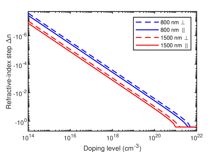
For doping levels above , the contrast reaches a saturation as the real part of the refractive index becomes zero. At this point the plasma frequency from Eq. (11) exceeds the frequency of the incident light and the material exhibits metallic reflection.
A.2 Wavelength independence for TE and TM waveguide modes
In this section we present an analysis that clarifies why the shape of the optical mode in the waveguide is nearly independent on wavelength of the light, for all cases where the associated optical frequency is well above the plasma frequency of the free carrier system, building on Refs. Bahaa E. A. Saleh, 2007; Hunsperger, 2009. In order to model the electric field distribution inside a planar waveguide, we have to consider the wave nature of light. For certain angles of reflection at the core-substrate and core-cladding interfaces the phase of the wave yields constructive interference with itself after the two reflections. In such cases the total field can be described by two particular plane waves that interfere with each other to generate a field distribution that is homogeneous along the propagation direction. These particular fields define the waveguide modes.
Reflection angle
The reflection angle for the mode (where is the lowest order mode) can be found using the mentioned self-consistency condition where the wave should reproduce itself every second reflection. For a dielectric waveguide, this condition is
| (15) |
where is the vacuum wavelength, the refractive index for the waveguide core, the thickness of the core, and is the phase that is accumulated upon reflection from the cladding (substrate) interface. The latter be found by solving the boundary value problem for the electromagnetic field at the core-cladding and core-substrate interfaces. For TE polarization it becomes
| (16) |
with the critical angle for total internal reflection on the cladding (substrate). Figure 7 shows the accumulated phase as a function of reflection angle , for 800 nm and 1000 nm light for the waveguide structures as mentioned in the main text. The total round-trip phase will not pass before the critical angle for total internal reflection on the core-substrate interface is reached. Therefore, this waveguide will only support the fundamental waveguide mode.
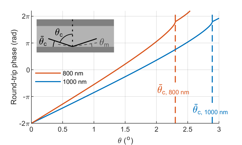
In fact, for the doping concentrations mentioned in the main text, this will be a single-mode waveguide for all wavelengths 111That is: for all frequencies below the bandgap and far enough above the plasma frequency. This is because the complement of the critical angle scales linearly with wavelength in the small-angle approximation for and binomial approximation for . The critical angle becomes
Therefore, the slower phase accumulation (Eq. (16)) at larger wavelengths is near-perfectly compensated by an increased .
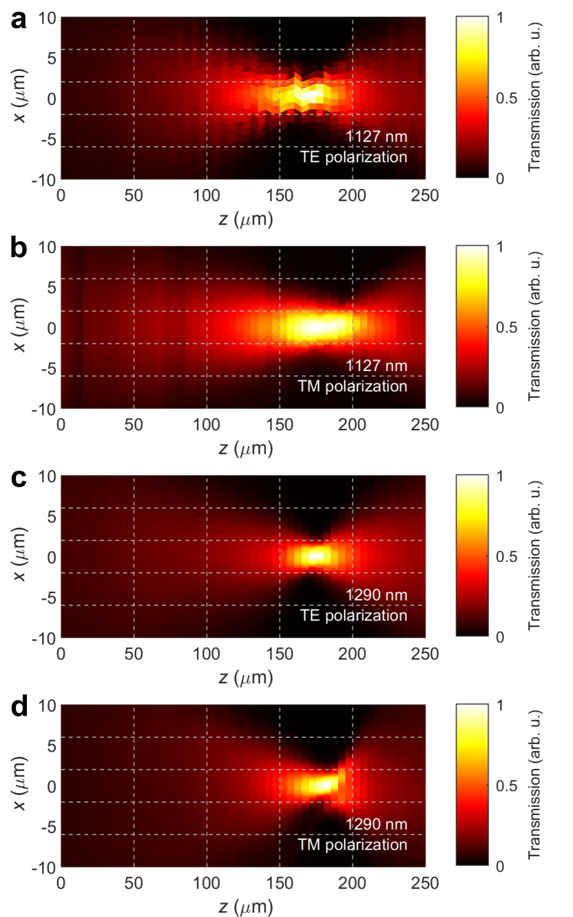
A.3 Additional results for mode-matching studies
Figure 8 presents experimental results for TM polarization and wavelengths in the range 700 to 1000 nm. An analysis of these mode-matching results is presented in Fig. 9. Figure 10 presents experimental results for both TE and TM polarization, for the wavelengths 1127 and 1290 nm.