Electronic and magnetic properties of silicene monolayer under bi-axial mechanical strain: first principles study
Abstract
Mechanical control of electronic and magnetic properties of 2D Van-der-Waals heterostructures gives new possibilities for further development of spintronics and information-related technologies. Using the density functional theory, we investigate the structural, electronic and magnetic properties of silicene monolayer with substituted Chromium atoms and under a small biaxial strain (). Our results indicate that the Cr-doped silicene nanosheets without strain have magnetic metallic, half-metallic or semiconducting properties depending on the type of substitution. We also show that the magnetic moments associated with the monomer and vertical dimer substitutions change very weakly with strain. However, the magnetic moment associated with the horizontal dimer substitution decreases when either compressive or tensile strain is applied to the system. Additionally, we show that the largest semiconductor band-gap is approximately 0.13 eV under zero strain for the vertical Cr-doped silicene. Finally, biaxial compressive strain leads to irregular changes in the magnetic moment for Cr vertical dimer substitution.
1 Introduction
Two-dimensional (2D) crystals are currently of great interest for both applied and fundamental research. The most prominent example of this kind materials is graphene. However, the class of 2D materials is very large and is continuously growing. It contains single-layered materials such as those belonging to the group IV of the periodic table (silicene, germanene and stanene) and to the group V (arsenene, antimonene, bismuthene), as well as layered 2D materials like Transition Metal Dichalcogenides and MXenes. Among them silicene seems to be a promising material due to its compatibility with existing silicon-based electronic devices. Because of sp3 hybridization, silicene is the 2D buckled hexagonal lattice of silicon atoms, and is considered as a one of alternative materials to graphene Greve et al. (2010); Enriquez et al. (2012); Feng et al. (2012); Lalmi et al. (2010); Tao et al. (2015). Research activities on silicene significantly increased after its successful synthesis under UHV conditions on several substrates, like for instance on Ag(111), ZrB2(0001), MoS2(0001), and Ir(111) Kumar & Ahluwalia (2013, 2012c, 2012a, 2012b); Mao et al. (2018). Silicene displays several interesting characteristics, which have been revealed by recent experimental and theoretical investigations. These include for instance: (i) a remarkable spin–orbit coupling parameter, that leads to the energy gap of 1.5 meV Chen (2016); Chowdhury & Jana (2016); Ding et al. (2017) at the Dirac point, which is much larger than that in graphene (24 eV) Enriquez et al. (2012); Drummond et al. (2012); Ezawa (2012); (ii) electrically tunable bandgap; (iii) the phase transition from a spin Hall topological insulator to a band insulator Dyrdał & Barnaś (2012); (iv) the strain-induced tunable bandgap Gmitra et al. (2009); Guo et al. (2015, 2013), and (v) promising electric and thermoelectric characteristics Wierzbicki et al. (2015a, b); Weymann et al. (2017); Krompiewski (2021); Krompiewski & Cuniberti (2017); Ghasemi et al. (2019); Jafari et al. (2020). The energy gap in silicene makes it promising for applications, however the realization of stabile monolayer of silicene is still problematic Low et al. (2011). For example, to achieve high on-to-off current ratios and a perfect switching capability, the material exploited for Field-Effect-Transistors (FETs) is usually required to have a fairly large bandgap Mao et al. (2018), significantly larger than that mentioned above for silicene.
Electronic and magnetic properties of silicene can be tuned by impurities, i.e., magnetic atoms built into the monolayer structure. Importantly, recent achievements of nanotechnology enable precise arrangements of impurities (including regular lattices), so by doping one can modify electronic properties in a controllable way. The single-side adsorption of alkali metal atoms on silicene has been reported to give rise to a bandgap of approximately 0.5 eV Zhang et al. (2013); Le Lay (2015), that is much larger than that due to intrinsic spin-orbit interaction. If both sides of the single-layer silicene have been saturated with hydrogen atoms, the formed composite system has been shown to be a kind of a nonmagnetic semiconductor Cao et al. (2015). Based on the previous studies, the ferromagnetic characteristics of silicene can be attributed to the single-side hydrogenation Zhang et al. (2012).
Strain engineering enables external control of electronic characteristics of semiconductor heterostructures and nanomaterials. This technique is widely applied to nano-electro-mechanical and nano-opto-mechanical systems, as well as to MOSFETs Chu et al. (2009); Lee et al. (2005). In turn, the in-plane strain in silicene leads to a modification of the electronic structure and its transport characteristics Qin et al. (2012); Farokhnezhad et al. (2017).
An important question is whether a significant gap in the spectrum of silicene can be induced by the strain, especially at low values of strain. If this is the case, tunable silicene devices would be of great practical importance. According to earlier density functional theory (DFT) calculations, a gap in the spectrum of silicene can be open under arbitrary uniaxial strain. Its magnitude varies non-monotonically with the strain. These findings were supported by other ab-initio (without empirical parameters and from first principles) calculation Mohan et al. (2014). For similar strain magnitudes, however, the two gap calculations were not in agreement. Recently, Pereira et al. Pereira et al. (2009) have questioned the accuracy of those conclusions by applying the Tight Binding (TB) approach. According to their findings, a spectral gap can only be achieved for +20% uniaxial deformations. Furthermore, this effect highly depends on the deformation route regarding the rudimentary lattice. The aforementioned findings are in accordance with the studies of Hasegawa et al. Hasegawa et al. (2006), indicating that there is a robust gapless Dirac spectrum with regard to arbitrary and not extremely large changes in the nearest neighbour hopping parameters. Moreover, employing the TB model, Wunsch et al. Wunsch et al. (2008) found that the semi-metallic phase appears for hopping parameter expansion.
The results of ab-initio calculations Farjam & Rafii-Tabar (2009) are in agreement with the gapless situation presented in Faccio et al. (2009). The inconsistency between various ab-initio calculations ware partially related to the fact that due to strain the Dirac points shift from the high symmetry points of the Brillouin zone. This resulted in arriving at the wrong conclusion that a bandgap is achievable for any strain. In addition, Faccio et al. also performed DFT research and calculated the impact of strain in silicene nanoribbon [43]. Keeping in mind that mechanical strain can substantially change the physical properties of silicene, we have performed detailed ab-initio calculations of the magnetic and electronic characteristics of silicene with inserted dimers and monomers of Cr atoms. Then, we have analysed the influence of a biaxial strain for up to deformations. We have shown that magnetic and electronic characteristics of silicene with substitutional impurity atoms can be easily controlled by various kinds of strains (i.e., substrate-induced strains or external mechanical forces). It is worth to note, that the gap due to strain and doping is significantly larger than the gap induced by the intrinsic spin-orbit interaction in undoped and unstrained silicene.
2 Methodology and strain-dependent structural properties
To study electronic and magnetic properties of silicene under mechanical strain we have used the DFT method Grimme et al. (2010) within the Perdew-Burke-Ernzerhof (PBE) generalized gradient approximation (GGA) Grimme (2006) form of the exchange-correlation functional, as implemented in the QuantumATK code package ver. S-2021.06 Stradi et al. (2016); Smidstrup et al. (2020). The PseudoDojo collection of optimized norm-conserving Vanderbilt (ONCV) pseudopotentials and ultra-basis set have been used for the optimization of structures and for further calculations van Setten et al. (2018). For the Brillouin zone integration we have taken 881 Monkhorst-Pack k-points in self-consisting calculation (SCF), and the mesh cut-off of energy has been set to 450 Ry. Structures ware relaxed until the forces on each atom were less than 0.05 eV/ and relative convergence for the Self-Consistent Field (SCF) energy is reached until eV/. We have used 15 vacuum region to prevent interaction of two neighboring layers along the -axis Ernzerhof & Scuseria (1999); Yin & Cohen (1982); Burke (2012).
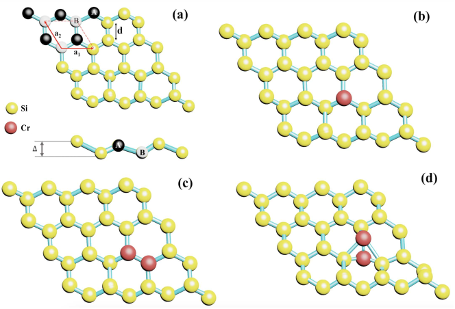
The atomic structure of silicene should be characterized before modelling the electronic structure L. C. (2015). The first structure optimization process for a single layer of Si was reported by Takeda and Shiraishi Takeda & Shiraishi (1994). By analogy to graphite, they defined a hexagonal lattice for Si atoms (with a periodicity perpendicular to the plane with a large vacuum layer of minimally 10 ), and then varied the in-plane lattice constant and positions of the basis atoms (Figure 1(a)) inside the unit cell, while keeping constant the imposed D3d symmetry 52. According to their results, the buckled structure has a lower total energy, with a local minimum for and a deformation angle of 9.9∘, when compared to the energy of a flat structure L. C. (2015).
In the present study, the 44 monolayer of silicene was characterized systematically (thus the unit cells were repeated up to four times in the and directions) using DFT Kansara et al. (2018). The Si atom bounded to three nearest neighbour surrounding Si atoms with the Si-Si bond length of and lattice parameter of was assumed prior to structural relaxation. The optimized lattice parameter, , correlates quite well with other data, even though the standard GGA functional method overestimates it. The buckling parameter is , which is also consistent with other studies Lebègue & Eriksson (2009); Björkman (2014); Yan et al. (2015); Ni et al. (2012); Liu et al. (2012).
In this paper we analyse three different types of substitution in silicene monolayer by Chromium adatoms as presented in Figure 1. These are: (i) monomer substitution, where one Si atom in the supercell is substituted by Cr atom ( substitution), as presented in Figure 1 (b); (ii) horizontal dimer (HDimer) substitution with two neighbouring Si atoms substituted by Cr atoms ( substitution), see Figure 1 (c); (iii) vertical dimer (VDimer) substitution, where one Si atom is replaced by two Cr atoms ( substitution), as shown in Figure 1 (d). These three structures were modeled within the optimized 44 supercell geometries, and we analysed behaviour of the electronic and magnetic properties with the strain.
The strain is defined as a deformation resulting from external loads or forces, that may be calculated by the following equation: with , where is the lattice parameter of the strained silicene and is the lattice constant of the unstrained silicene Qin et al. (2012); Mohan et al. (2014); Kaloni et al. (2013). The model of strained unit cell for the tensile and compression strains is achieved by varying the lattice constant along the lattice vectors by the following substitution . Accordingly, the uniaxial tensile strain or compression ( respectively) is realized by modification of the lattice constant in the direction, that is by modification of the lattice vector (mechanical force applied along the lattice vector ), whereas the biaxial tensile or compressive strain is described by modification of both and lattice vectors (forces are oriented along both lattice vectors).
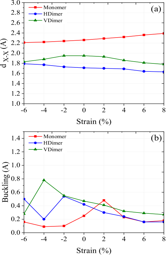
The presence of biaxial strain affects the buckling parameter, , as well as the Cr-Si and Cr-Cr bonds in the silicene monolayer with monomer and dimer substitutions, respectively. Figure 2 presents the basic parameters of the relaxed structures as a function of strain and also for all the substitutions under consideration.
For the monomer substitution (see Figures 2(a)), the bond length between Cr and Si atoms, , slightly increases with the strain. However, there is no clear universal behavior of the buckling parameter with strain, though one can see that this parameter reaches a maximum for a specific strain equal , and then decreases with increasing magnitude of either tensile or compressive strain.
For the silicene with HDimer substitution, the tensile strain reduces monotonically the bond length and the buckling parameter. However, for the compressive strain one observes increase of the bond length for Cr-Cr dimers. In turn, the buckling parameter for Cr-Cr HDimers varies nonmonotonously with the magnitude of compressive strain, i.e., it reaches a minimum at some magnitude of the strain, see Figure 2(b).
In turn, for the VDimer substitution, the strain only very slightly affects the bound lengths reducing it when the strain takes absolute values larger than 2. The corresponding buckling parameter decreases with increasing tensile strain and increases with increasing magnitude of the compressive strain up to , where it reaches a maximal value, and then decreases with a further increase of the magnitude of compressive strain.
At this point, one should note that high strain values are experimentally difficult to obtain. Mohan et al. (2014); Mohiuddin et al. (2009); Tsoukleri et al. (2009); Huang et al. (2010); Bertolazzi et al. (2011); Fischetti & Laux (1996). The recent reports about graphene-like monoatomic crystals indicate that the strain around can be relatively easily obtained. Accordingly, in this paper we have restricted our considerations to the strain ranging from to .
3 Strain-dependent electronic and magnetic properties
It is well known that strain has a significant impact on electronic and magnetic properties of 2D crystals Roldán et al. (2015); Wang et al. (2015); Si et al. (2016); Khatibi et al. (2019a, b). One of the consequences of the strain in 2D crystal is the electronic bandgap engineering, i.e., strain-induced bandgap opening Wierzbicki et al. (2015a) or a direct–indirect–direct bandgap transition in green phosphorene Peng et al. (2014); Shao et al. (2017).
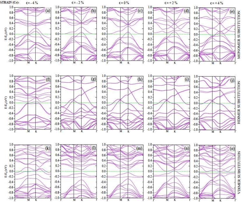
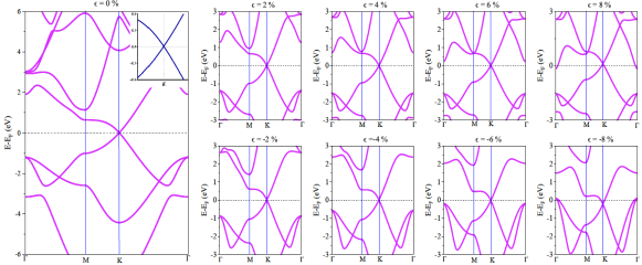
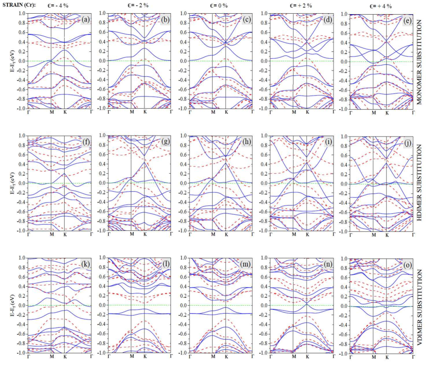
Figure 3 presents the band structures of strained and unstrained silicene doped with Cr for the three different types of substitution (Monomer, HDimer and VDimer), as discussed in Section 2. The band structure has been calculated along the high-symmetry points of the Brillouin zone, i.e., along the -M–K– path. In turn, Table 1 collects information about the band gap in silicene under strain and with different types of Cr substitution. The electronic band structure of undoped silicene monolayer under strain is presented in A. Here one needs to remind, that strain in undoped silicene does not open a gap. A small gap appears only due to spin-orbit interaction. When neglecting this interaction, the gap in undoped silicene remains equal to zero (at the Dirac points), see also Figure 5 in Appendix A. Apart from this, due to hybridization of the 3d-impurity states and those of pure silicene, the band structure becomes remarkably modified by doping. Each state of the doped system includes in general contributions due to 3d-transition metals as well as due to silicon atoms. To show this explicitly, we have presented the so-called fat-bands structure, where the two contributions are indicated explicitly with different colors. In B we present fat-bands calculated for silicene monolayer doped with Cr-atoms (i.e., the band structure projected over orbitals of Silicone and Chromium atoms). The corresponding results are shown in Figure 6, and from this figure one can estimate whether a particular band contributes to conductivity or not. If it is due to impurities only and is dispersionless around the Fermi level, it does not contribute to conductivity. If however it is dispersive around the Fermi level, then even though the silicon contribution is small, it contributes to conductivity. These features have been taken into account when determining the band gaps. In B we show the fat-bands for silicene with Cr-Monomers, Cr-HDimers and Cr-VDimers.
The silicene with Cr-monomers is either metallic or semimetallic, with the Fermi energy crossing the valence bands. In the presence of compressive strain the energy gap becomes opened in the spectrum above the Fermi energy, while the Fermi level is still inside the valence bands. In the presence of tensile strain the system moves from semimetallic to metallic one. In turn, for silicene with Cr-HDimer substitution, the electronic structure is only slightly affected by the strain. The most promising effect of strain on the electronic structure can be observed for silicene monolayer with Cr-VDimer substitution. Without strain the system is a semiconductor with the energy gap equal 0.13 eV. Applying compressive strain one can close the energy gap and move the Fermi level to the valence bands. The tensile strain, in turn, leads to reduction of the energy gap for the 4 strain, and leads to its complete closure for strain .
| Strain (%) | -6% | -4% | -2% | 0% | 2% | 4% | 6% | 8% |
| Monomer-Cr | 0 | 0 | 0 | 0 | 0 | 0 | 0 | 0 |
| HDimer-Cr | 0.1 | 0 | 0 | 0 | 0 | 0 | 0 | 0 |
| VDimer-Cr | 0 | 0 | 0.12 | 0.13 | 0 | 0.05 | 0 | 0 |
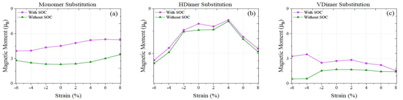
Our calculations also reveal the impact of biaxial strain on the magnetic characteristics of the silicene monolayer doped with the specified above Monomers, HDimers and VDimers of Cr atoms. The corresponding results are presented in Figure 4, where spin polarization of silicene monolayer doped with Cr atoms is shown as a function of strain (the three types of substitution are presented). Situations in the presence of spin-orbit interaction and that in the absence of spin-orbit coupling are shown there. In the latter case, the calculation procedure is described in C. For silicene with the Cr-monomers, the magnetic moment varies monotonously with the strain when the spin-orbit coupling is included, while in its absence, the magnetic moment increases with the magnitude of strain, both tensile and compressive. Moreover, the difference between these two situations is relatively large. In turn, for the case of Cr-HDimer, the magnetic moment decreases with the compressive and tensile strain, and the difference between the cases with and without spin-orbit interaction is small. For the silicene monolayer doped with Cr-VDimers, the magnetic moment only weakly depends on the strain for strain larger than , and the difference between the case with and without spin-orbit interaction is small except the strain below , where this difference is relatively large. It is worth noting that the largest magnetic moment for the unstrained system is for silicene monolayer with Cr-HDimers, where the changes in the magnetic moment due to strain are also most pronounced.
4 Conclusions
In this work we presented detailed study of electronic and magnetic properties of silicene doped with Cr atoms in one of the three doping schemes, i.e., monomer, HDimer, and VDimer substitutions. Numerical results based on the DFT calculations clearly show that the way of substitution may substantially change the structural, electronic and magnetic behaviour of the silicene under strain. The interplay of doping and strain may be used to engineer band gap, and thus also character of transport properties from metallic to half-metallic or semiconducting.
Such a strain-induced engineering of transport properties is important from the practical point of view as it may be used in various spintronics and/or logic devices. It is expected, that controlling current and magnetic state with a strain opens new route for nanoelectronics of future generation.
5 Acknowledgments
We thank Prof. J. Barnaś for valuable discussions and reading this manuscript. This work has been supported by the Norwegian Financial Mechanism 2014- 2021 under the Polish-Norwegian Research Project NCN GRIEG “2Dtronics” no. 2019/34/H/ST3/00515.
Appendix A The electronic band structure of undoped silicene
To understand the interplay of the effects due to strain and doping, it is advisory to analyse the impact of strain on the undoped silicene. In Figure 5 we present the electronic structure of pure silicene monolayer subject to a biaxial strain from to , and in the absence of spin-orbit coupling. It is evident, that the strain has a significant a impact on the band structure. However, the band gap remains zero as in the absence of strain. The valence and conduction bands tough each other at the Dirac K points, independently of the strain, which preserves semi-metallic behavior of the system with increasing strain, either tensile or compressive. The strain does not open a gap, however, it modifies asymmetry of the Dirac cones.
Appendix B The fat-band structures
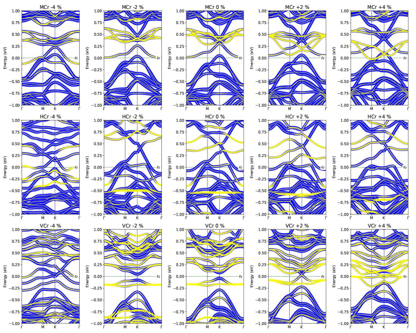
As already mentioned above, due to hybridization of the 3d-impurity states and those of pure silicene, the band structure becomes remarkably modified by doping. Each state of the doped system includes then, in general, contributions from the 3d-transition metals as well as due to the silicon atoms. We show this explicitly in Figure 6, where the two contributions are indicated with different colors for silicene monolayer doped with Cr-atoms. We show there the fat-bands for Cr-Monomers, Cr-HDimers and Cr-VDimers. From this figure one can evaluate whether a particular band contributes to transport or not, and this was taken into account when determining the band gaps presented in Table 1.
Appendix C The electronic band structure of silicene doped by Cr atoms from collinear calculations
In this section we present electronic spectrum of silicene monolayer doped by Cr atoms in the presence of biaxial strain. As before we consider the three types of substitutions discussed in the main text. The electronic structure has been obtained from collinear (spin polarized) calculations. This procedure is applicable in the absence of spin-orbit interaction, where spin-up and spin-down states are well defined. Figure 7 presents the corresponding electronic band dispersions, where the solid blue and dashed red lines correspond to the spin-up and spin-down states, respectively.
References
- Bertolazzi et al. (2011) Bertolazzi, S., Brivio, J., & Kis, A. 2011, ACS Nano, 5, 9703, doi: 10.1021/nn203879f
- Björkman (2014) Björkman, T. 2014, The Journal of Chemical Physics, 141, 074708, doi: 10.1063/1.4893329
- Burke (2012) Burke, K. 2012, The Journal of Chemical Physics, 136, 150901, doi: 10.1063/1.4704546
- Cao et al. (2015) Cao, G., Zhang, Y., & Cao, J. 2015, Physics Letters A, 379, 1475, doi: 10.1016/j.physleta.2015.03.021
- Chen (2016) Chen, S.-H. 2016, Journal of Magnetism and Magnetic Materials, 405, 317, doi: 10.1016/j.jmmm.2015.12.088
- Chowdhury & Jana (2016) Chowdhury, S., & Jana, D. 2016, Reports on Progress in Physics, 79, 126501, doi: 10.1088/0034-4885/79/12/126501
- Chu et al. (2009) Chu, M., Sun, Y., Aghoram, U., & Thompson, S. E. 2009, Annual Review of Materials Research, 39, 203, doi: 10.1146/annurev-matsci-082908-145312
- Ding et al. (2017) Ding, N., Wang, H., Chen, X., & Lawrence Wu, C.-M. 2017, RSC Advances, 7, 10306, doi: 10.1039/C6RA27291F
- Drummond et al. (2012) Drummond, N. D., Zólyomi, V., & Fal’ko, V. I. 2012, Physical Review B, 85, 075423, doi: 10.1103/PhysRevB.85.075423
- Dyrdał & Barnaś (2012) Dyrdał, A., & Barnaś, J. 2012, physica status solidi (RRL) - Rapid Research Letters, 6, 340, doi: 10.1002/pssr.201206202
- Enriquez et al. (2012) Enriquez, H., Vizzini, S., Kara, A., Lalmi, B., & Oughaddou, H. 2012, Journal of Physics: Condensed Matter, 24, 314211, doi: 10.1088/0953-8984/24/31/314211
- Ernzerhof & Scuseria (1999) Ernzerhof, M., & Scuseria, G. E. 1999, The Journal of Chemical Physics, 110, 5029, doi: 10.1063/1.478401
- Ezawa (2012) Ezawa, M. 2012, Physical Review Letters, 109, 055502, doi: 10.1103/PhysRevLett.109.055502
- Faccio et al. (2009) Faccio, R., Denis, P. A., Pardo, H., Goyenola, C., & Mombrú, Á. W. 2009, Journal of Physics: Condensed Matter, 21, 285304, doi: 10.1088/0953-8984/21/28/285304
- Farjam & Rafii-Tabar (2009) Farjam, M., & Rafii-Tabar, H. 2009, Physical Review B, 80, 167401, doi: 10.1103/PhysRevB.80.167401
- Farokhnezhad et al. (2017) Farokhnezhad, M., Esmaeilzadeh, M., & Shakouri, K. 2017, Physical Review B, 96, 205416, doi: 10.1103/PhysRevB.96.205416
- Feng et al. (2012) Feng, B., Ding, Z., Meng, S., et al. 2012, Nano Letters, 12, 3507, doi: 10.1021/nl301047g
- Fischetti & Laux (1996) Fischetti, M. V., & Laux, S. E. 1996, Journal of Applied Physics, 80, 2234, doi: 10.1063/1.363052
- Ghasemi et al. (2019) Ghasemi, N., Ahmadkhan Kordbacheh, A., & Berahman, M. 2019, Journal of Magnetism and Magnetic Materials, 473, 306, doi: 10.1016/j.jmmm.2018.10.059
- Gmitra et al. (2009) Gmitra, M., Konschuh, S., Ertler, C., Ambrosch-Draxl, C., & Fabian, J. 2009, Physical Review B, 80, 235431, doi: 10.1103/PhysRevB.80.235431
- Greve et al. (2010) Greve, H., Woltermann, E., Quenzer, H.-J., Wagner, B., & Quandt, E. 2010, Applied Physics Letters, 96, 182501, doi: 10.1063/1.3377908
- Grimme (2006) Grimme, S. 2006, Journal of Computational Chemistry, 27, 1787, doi: 10.1002/jcc.20495
- Grimme et al. (2010) Grimme, S., Antony, J., Ehrlich, S., & Krieg, H. 2010, The Journal of Chemical Physics, 132, 154104, doi: 10.1063/1.3382344
- Guo et al. (2015) Guo, X.-X., Guo, P., Zheng, J.-M., Cao, L.-K., & Zhao, P.-J. 2015, Applied Surface Science, 341, 69, doi: 10.1016/j.apsusc.2015.03.002
- Guo et al. (2013) Guo, Z.-X., Furuya, S., Iwata, J.-i., & Oshiyama, A. 2013, Physical Review B, 87, 235435, doi: 10.1103/PhysRevB.87.235435
- Hasegawa et al. (2006) Hasegawa, Y., Konno, R., Nakano, H., & Kohmoto, M. 2006, Physical Review B, 74, 033413, doi: 10.1103/PhysRevB.74.033413
- Huang et al. (2010) Huang, M., Yan, H., Heinz, T. F., & Hone, J. 2010, Nano Letters, 10, 4074, doi: 10.1021/nl102123c
- Jafari et al. (2020) Jafari, M. A., Kordbacheh, A. A., Mahdian, S., & Ghasemi, N. 2020, Physica E: Low-dimensional Systems and Nanostructures, 117, 113855, doi: 10.1016/j.physe.2019.113855
- Kaloni et al. (2013) Kaloni, T. P., Cheng, Y. C., & Schwingenschlögl, U. 2013, Journal of Applied Physics, 113, 104305, doi: 10.1063/1.4794812
- Kansara et al. (2018) Kansara, S., Gupta, S. K., & Sonvane, Y. 2018, Computational Materials Science, 141, 235, doi: 10.1016/j.commatsci.2017.09.037
- Khatibi et al. (2019a) Khatibi, Z., Namiranian, A., & Panahi, S. 2019a, Physica B: Condensed Matter, 565, 33, doi: 10.1016/j.physb.2018.11.029
- Khatibi et al. (2019b) Khatibi, Z., Namiranian, A., & Parhizgar, F. 2019b, Diamond and Related Materials, 92, 228, doi: 10.1016/j.diamond.2018.12.007
- Krompiewski (2021) Krompiewski, S. 2021, Journal of Magnetism and Magnetic Materials, 534, 168036, doi: 10.1016/j.jmmm.2021.168036
- Krompiewski & Cuniberti (2017) Krompiewski, S., & Cuniberti, G. 2017, Physical Review B, 96, 155447, doi: 10.1103/PhysRevB.96.155447
- Kumar & Ahluwalia (2012a) Kumar, A., & Ahluwalia, P. 2012a, Materials Chemistry and Physics, 135, 755, doi: 10.1016/j.matchemphys.2012.05.055
- Kumar & Ahluwalia (2012b) —. 2012b, Physica B: Condensed Matter, 407, 4627, doi: 10.1016/j.physb.2012.08.034
- Kumar & Ahluwalia (2013) —. 2013, Physica B: Condensed Matter, 419, 66, doi: 10.1016/j.physb.2013.03.029
- Kumar & Ahluwalia (2012c) Kumar, A., & Ahluwalia, P. K. 2012c, The European Physical Journal B, 85, 186, doi: 10.1140/epjb/e2012-30070-x
- L. C. (2015) L. C., L. Y. V. 2015, Chinese Physics B, 24, 087309, doi: 10.1088/1674-1056/24/8/087309
- Lalmi et al. (2010) Lalmi, B., Oughaddou, H., Enriquez, H., et al. 2010, Applied Physics Letters, 97, 223109, doi: 10.1063/1.3524215
- Le Lay (2015) Le Lay, G. 2015, Nature Nanotechnology, 10, 202, doi: 10.1038/nnano.2015.10
- Lebègue & Eriksson (2009) Lebègue, S., & Eriksson, O. 2009, Physical Review B, 79, 115409, doi: 10.1103/PhysRevB.79.115409
- Lee et al. (2005) Lee, M. L., Fitzgerald, E. A., Bulsara, M. T., Currie, M. T., & Lochtefeld, A. 2005, Journal of Applied Physics, 97, 011101, doi: 10.1063/1.1819976
- Liu et al. (2012) Liu, G., Wu, M. S., Ouyang, C. Y., & Xu, B. 2012, EPL (Europhysics Letters), 99, 17010, doi: 10.1209/0295-5075/99/17010
- Low et al. (2011) Low, T., Guinea, F., & Katsnelson, M. I. 2011, Physical Review B, 83, 195436, doi: 10.1103/PhysRevB.83.195436
- Mao et al. (2018) Mao, Y., Xu, H., Yuan, J., & Zhong, J. 2018, Journal of Physics: Condensed Matter, 30, 365001, doi: 10.1088/1361-648X/aad6f9
- Mohan et al. (2014) Mohan, B., Kumar, A., & Ahluwalia, P. 2014, Physica E: Low-dimensional Systems and Nanostructures, 61, 40, doi: 10.1016/j.physe.2014.03.013
- Mohiuddin et al. (2009) Mohiuddin, T. M. G., Lombardo, A., Nair, R. R., et al. 2009, Physical Review B, 79, 205433, doi: 10.1103/PhysRevB.79.205433
- Ni et al. (2012) Ni, Z., Liu, Q., Tang, K., et al. 2012, Nano Letters, 12, 113, doi: 10.1021/nl203065e
- Peng et al. (2014) Peng, X., Wei, Q., & Copple, A. 2014, Physical Review B, 90, 085402, doi: 10.1103/PhysRevB.90.085402
- Pereira et al. (2009) Pereira, V. M., Castro Neto, A. H., & Peres, N. M. R. 2009, Physical Review B, 80, 045401, doi: 10.1103/PhysRevB.80.045401
- Qin et al. (2012) Qin, R., Wang, C.-H., Zhu, W., & Zhang, Y. 2012, AIP Advances, 2, 022159, doi: 10.1063/1.4732134
- Roldán et al. (2015) Roldán, R., Castellanos-Gomez, A., Cappelluti, E., & Guinea, F. 2015, Journal of Physics: Condensed Matter, 27, 313201, doi: 10.1088/0953-8984/27/31/313201
- Shao et al. (2017) Shao, C., Yu, X., Yang, N., Yue, Y., & Bao, H. 2017, Nanoscale and Microscale Thermophysical Engineering, 21, 201, doi: 10.1080/15567265.2017.1286421
- Si et al. (2016) Si, C., Sun, Z., & Liu, F. 2016, Nanoscale, 8, 3207, doi: 10.1039/C5NR07755A
- Smidstrup et al. (2020) Smidstrup, S., Markussen, T., Vancraeyveld, P., et al. 2020, Journal of Physics: Condensed Matter, 32, 015901, doi: 10.1088/1361-648X/ab4007
- Stradi et al. (2016) Stradi, D., Martinez, U., Blom, A., Brandbyge, M., & Stokbro, K. 2016, Physical Review B, 93, 155302, doi: 10.1103/PhysRevB.93.155302
- Takeda & Shiraishi (1994) Takeda, K., & Shiraishi, K. 1994, Physical Review B, 50, 14916, doi: 10.1103/PhysRevB.50.14916
- Tao et al. (2015) Tao, L., Cinquanta, E., Chiappe, D., et al. 2015, Nature Nanotechnology, 10, 227, doi: 10.1038/nnano.2014.325
- Tsoukleri et al. (2009) Tsoukleri, G., Parthenios, J., Papagelis, K., et al. 2009, Small, 5, 2397, doi: 10.1002/smll.200900802
- van Setten et al. (2018) van Setten, M., Giantomassi, M., Bousquet, E., et al. 2018, Computer Physics Communications, 226, 39, doi: 10.1016/j.cpc.2018.01.012
- Wang et al. (2015) Wang, X., Tantiwanichapan, K., Christopher, J. W., Paiella, R., & Swan, A. K. 2015, Nano Letters, 15, 5969, doi: 10.1021/acs.nanolett.5b02107
- Weymann et al. (2017) Weymann, I., Zwierzycki, M., & Krompiewski, S. 2017, Physical Review B, 96, 115452, doi: 10.1103/PhysRevB.96.115452
- Wierzbicki et al. (2015a) Wierzbicki, M., Barnaś, J., & Swirkowicz, R. 2015a, Physical Review B, 91, 165417, doi: 10.1103/PhysRevB.91.165417
- Wierzbicki et al. (2015b) —. 2015b, Journal of Physics: Condensed Matter, 27, 485301, doi: 10.1088/0953-8984/27/48/485301
- Wunsch et al. (2008) Wunsch, B., Guinea, F., & Sols, F. 2008, New Journal of Physics, 10, 103027, doi: 10.1088/1367-2630/10/10/103027
- Yan et al. (2015) Yan, J.-A., Gao, S.-P., Stein, R., & Coard, G. 2015, Physical Review B, 91, 245403, doi: 10.1103/PhysRevB.91.245403
- Yin & Cohen (1982) Yin, M. T., & Cohen, M. L. 1982, Physical Review B, 25, 7403, doi: 10.1103/PhysRevB.25.7403
- Zhang et al. (2012) Zhang, P., Li, X., Hu, C., Wu, S., & Zhu, Z. 2012, Physics Letters A, 376, 1230, doi: 10.1016/j.physleta.2012.02.030
- Zhang et al. (2013) Zhang, X.-L., Liu, L.-F., & Liu, W.-M. 2013, Scientific Reports, 3, 2908, doi: 10.1038/srep02908