Gradient-Based Optimization of Optical Vortex Beam Emitters
Abstract
Vortex beams are stable solutions of Maxwell’s equations that carry phase singularities and orbital angular momentum, unique properties that give rise to many applications in the basic sciences, optical communications, and quantum technologies. Scalable integration and fabrication of vortex beam emitters will allow these applications to flourish and enable new applications not possible with traditional optics. Here we present a general framework to generate integrated vortex beam emitters using photonic inverse design. We experimentally demonstrate generation of vortex beams with angular momentum spanning -3 to 3. We show the generality of this design procedure by designing a vortex beam multiplexer capable of exciting a custom vortex beam fiber. Finally, we produce foundry-fabricated beam emitters with wide-bandwidths and high-efficiencies that take advantage of a multi-layer heterogeneous integration.
Optical vortex beams and the orbital angular momentum (OAM) they carry are useful in a vast array of applications including classical and quantum communication, super-resolution microscopy, optical trapping and manipulation, and metrology Ni et al. (2021); Shen et al. (2019); Barreiro et al. (2008); Wang et al. (2012); Ren et al. (2016). While these beams are traditionally generated by phase plates or spatial light modulators, efforts have been made to integrate optical vortex beams emitters onto nanophotonic platforms. Such integration allows for the construction of extremely compact vortex beam generators in platforms that can provide additional functionality and optical processing.
Initial demonstrations of on-chip vortex beam generators consisted of ring resonators with gratings whose periodicity mismatch with the optical mode enforced the radial phase required for an OAM beam Cai et al. (2012). While this design is capable of producing high quality OAM beams in a compact area, the resonant nature of the devices limit their bandwidth and prevent multiplexing. Since then, many strategies for on-chip vortex beam generation have been demonstrated including OAM lasers Miao et al. (2016); Liu et al. (2017); Kitamura et al. (2019); Bahari et al. (2021), metasurfaces Yu et al. (2011); Chen et al. (2018); Sedeh et al. (2020), and analytical Su et al. (2012); Zhou et al. (2019); Zhao and Fan (2020) and computational Xie et al. (2018); Song et al. (2020); White et al. (2021) grating design.
Here we provide a general framework for the design of integrated vortex beam emitters using adjoint optimized photonics inverse design. We first demonstrate OAM beam generation of to in single layer silicon photonics. We then show a 3 mode OAM multiplexer designed to launch modes into a custom fiber. Finally, we utilize the well controlled fabrication and heterogeneous integration of a commercial foundry (A*STAR, AMF) to demonstrate high fidelity, wide bandwidth, and efficient vortex beam emitters. While we focus on vortex beam generation here, the same inverse design protocol can be used to optimize beam emitters and multiplexers for arbitrary free space modes.
Vortex beams consist of a Laguerre-Gaussian field profile with a phase that is linearly proportional to the angle and integrates to 2 times an integer , the orbital angular momentum:
| (1) |
where is the radial index and is the beam waist. For first order radial modes, the simplest OAM beams, this profile simplifies to
| (2) |
examples of which are shown in Figure 1a. Vortex beams can have nearly arbitrary polarization, including topologically interesting spatially varying polarization coupled with the beam shape Bauer et al. (2015), but here we use spatially homogeneous linear polarization for simplicity.
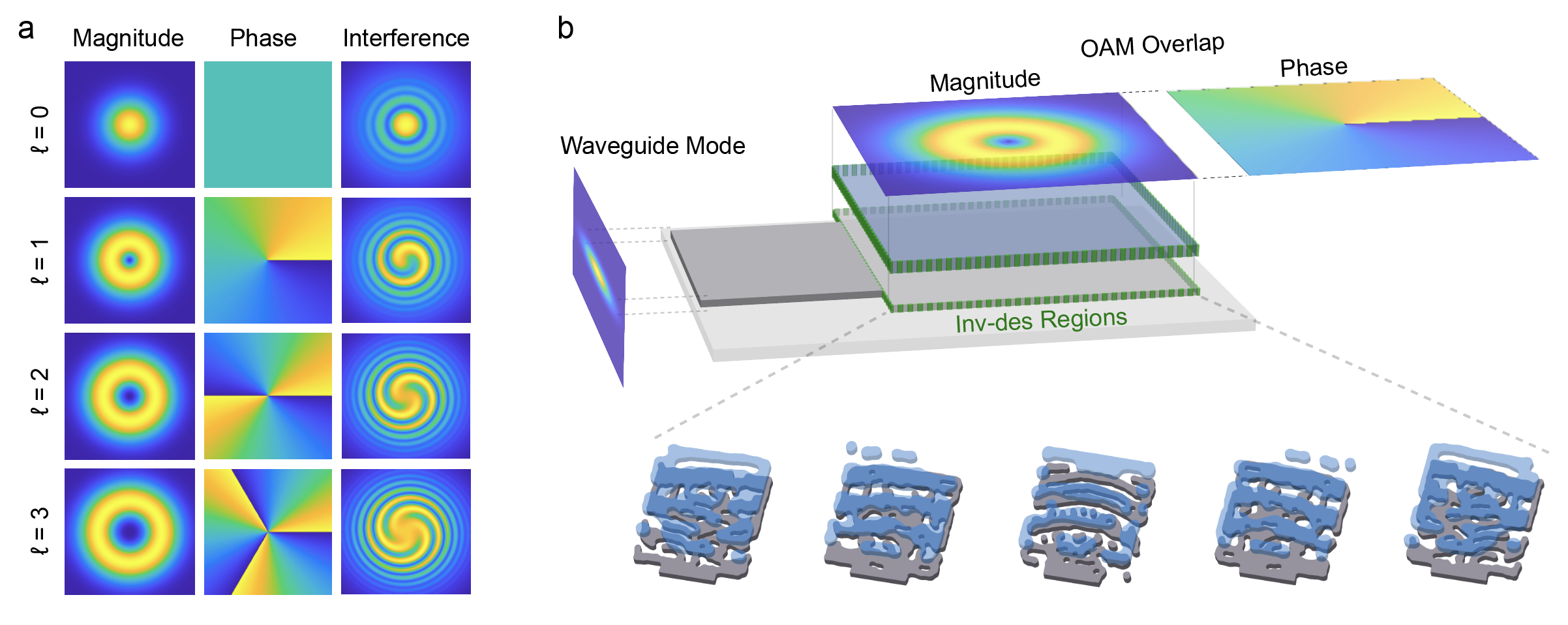
To design arbitrary beam emitters, we optimize a structure that takes a waveguide mode as input and launches a beam out of the plane of the chip whose electric field overlaps maximally with the desired beam shape in free space (Figure 1b). To efficiently optimize the structure, we use an adjoint optimization approach which allows us to calculate the optimization gradients at every point with only two simulations Goos (2021); Su et al. (2020). Here we optimize the emitters to form vortex beams, but this design approach is general and can be applied to any desired spatial field pattern.
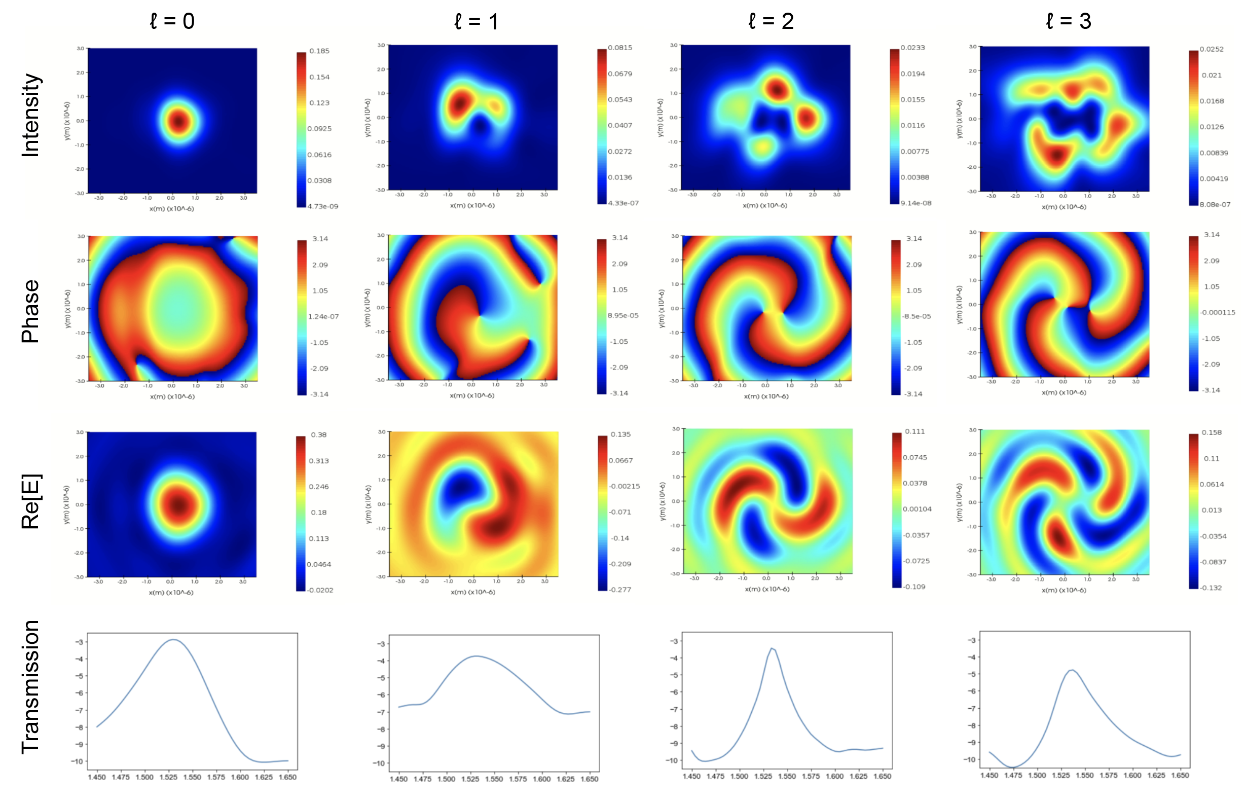
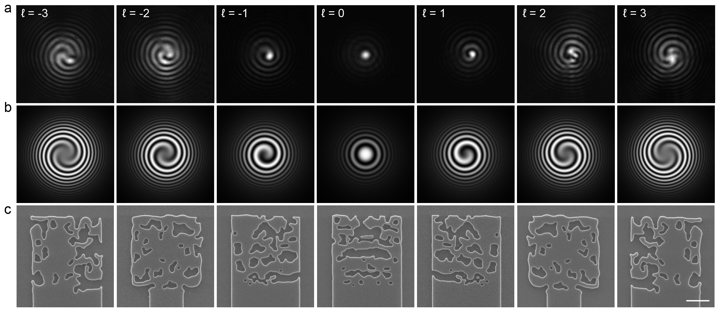
We first optimize compact devices that emit vortex beams for to . These devices are m and fabricated using electron beam lithography on an air-clad 220 nm silicon-on-insulator platform. They operate in the telecom band, and are designed with an 80 nm minimum feature size. To measure the emission properties, we excite an on-chip waveguide coupled to a device and collect the emitted light through a high NA objective. We then interfere the beam from the device with a Gaussian beam generated from the same laser source and image the resulting intensity pattern. Figure 2 shows the theoretical interference patterns from ideal vortex beams as well as the measured interference patterns (with simulations shown in Supplemental Figure 1). The spiral pattern is formed by the combination of a curved phase front radially and the angular OAM phase; the direction of spiraling shows the sign of the OAM and the number of teeth show the OAM order.
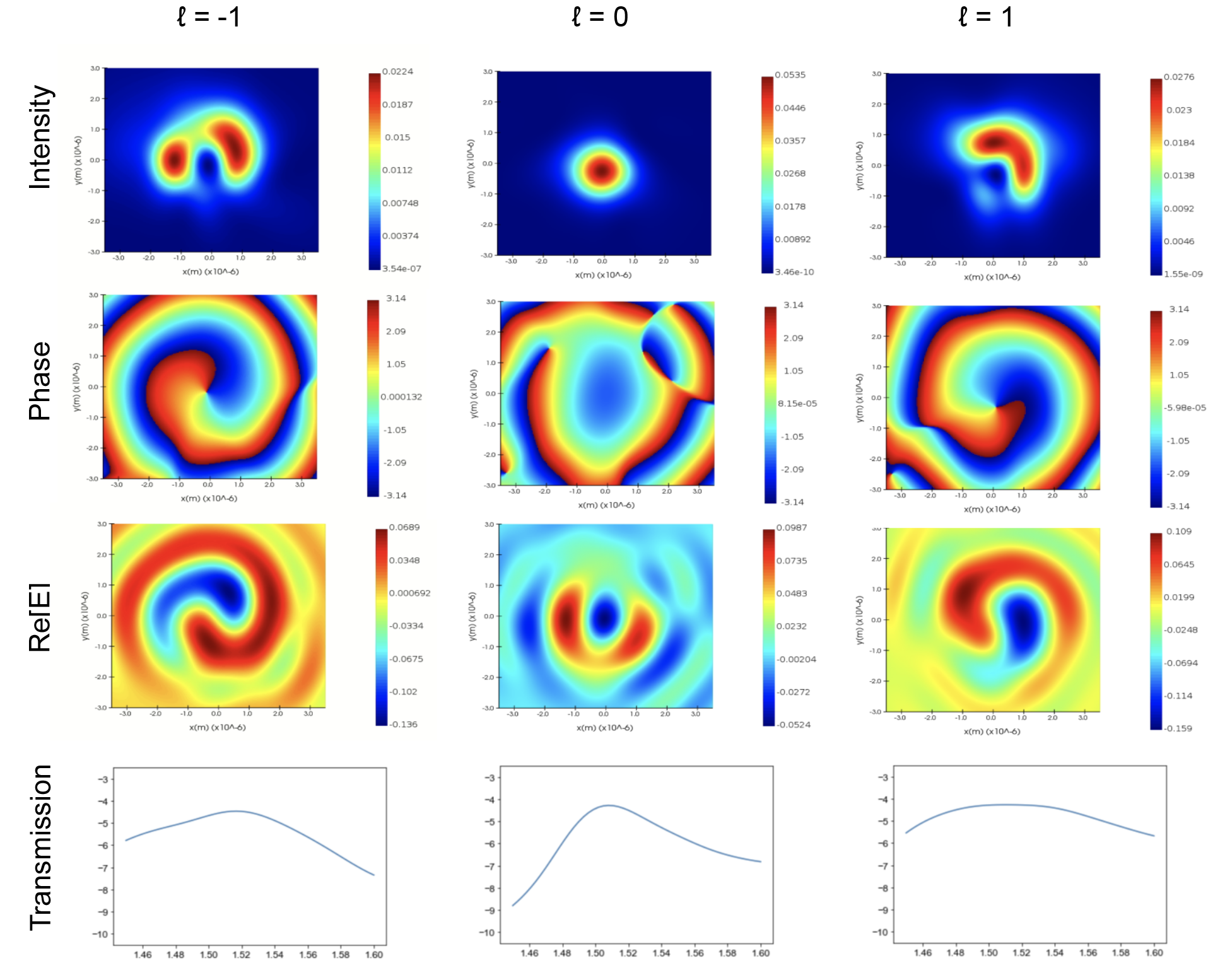
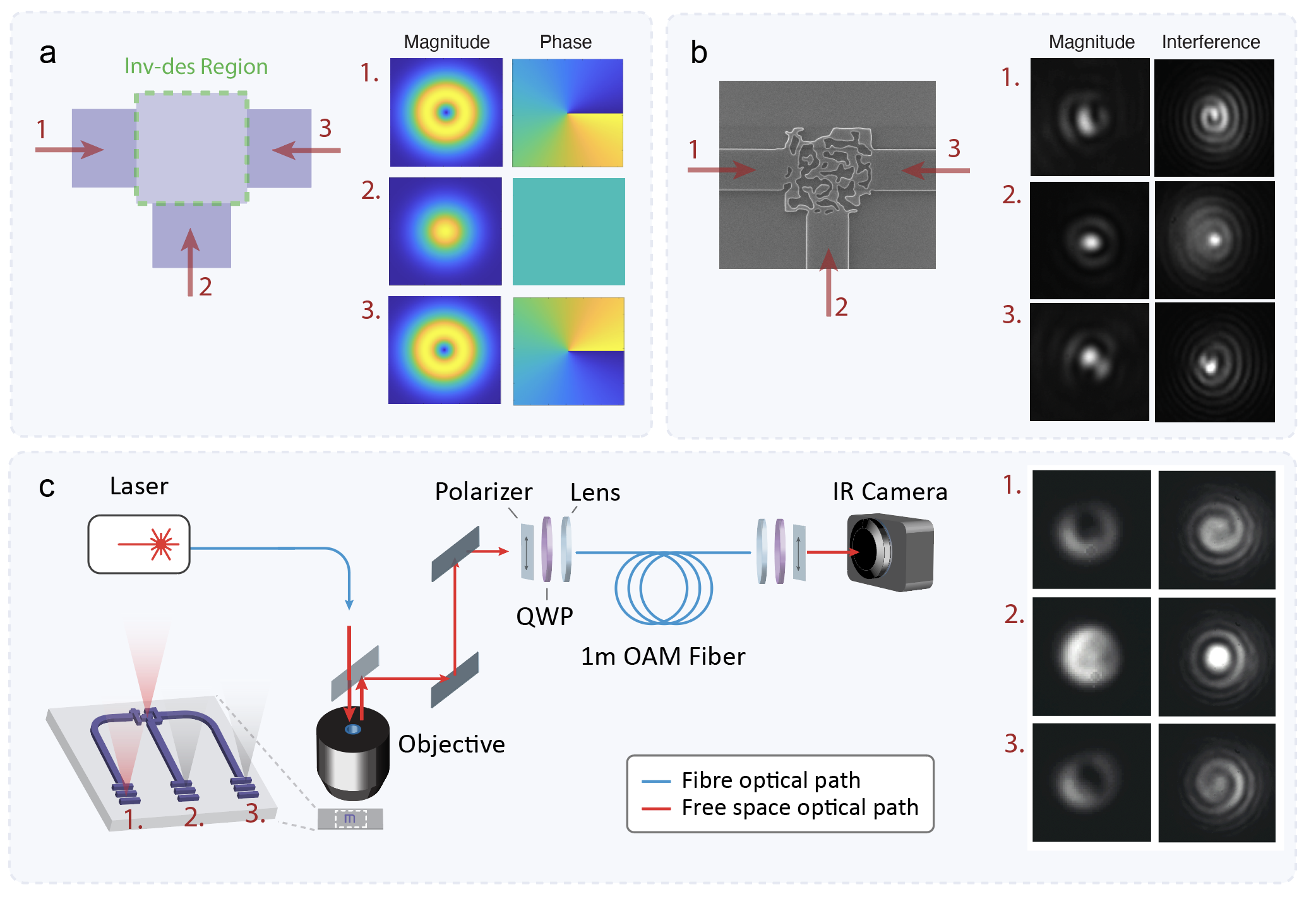
To demonstrate the generality of this design approach, we optimize a device to launch multiplexed modes into a custom OAM supporting optical fiber Bozinovic et al. (2013). The device is designed to launch an mode when excited from the left waveguide, when excited from the right, and when excited from the bottom waveguide (Figure 3a). Additionally, all of these modes are designed to be y-polarized so that a polarizer can be used to filter out undesired mode coupling in the fiber. This leads to the additional design complication that the mode must be launched with the orthogonal polarization to its input waveguide mode. Even with these additional constraints, the optimization procedure yielded a compact m device that was able to generate all 3 modes (Figure 3b, Supplemental Figure 2). To launch these modes into a custom OAM fiber, we pass the output fields through a polarizer and quarter wave plate to match the circularly polarized eigenmodes of the fiber, and use a lens to focus the collimated beams on the fiber core. To image the fiber modes with a camera, we employ another lens, quarter wave plate, and polarization beamsplitter (Figure 3c). This leads to beams which are even more pure than those directly from the multiplexer, as the fiber filters out any higher order modes from design nonidealities and scattering.
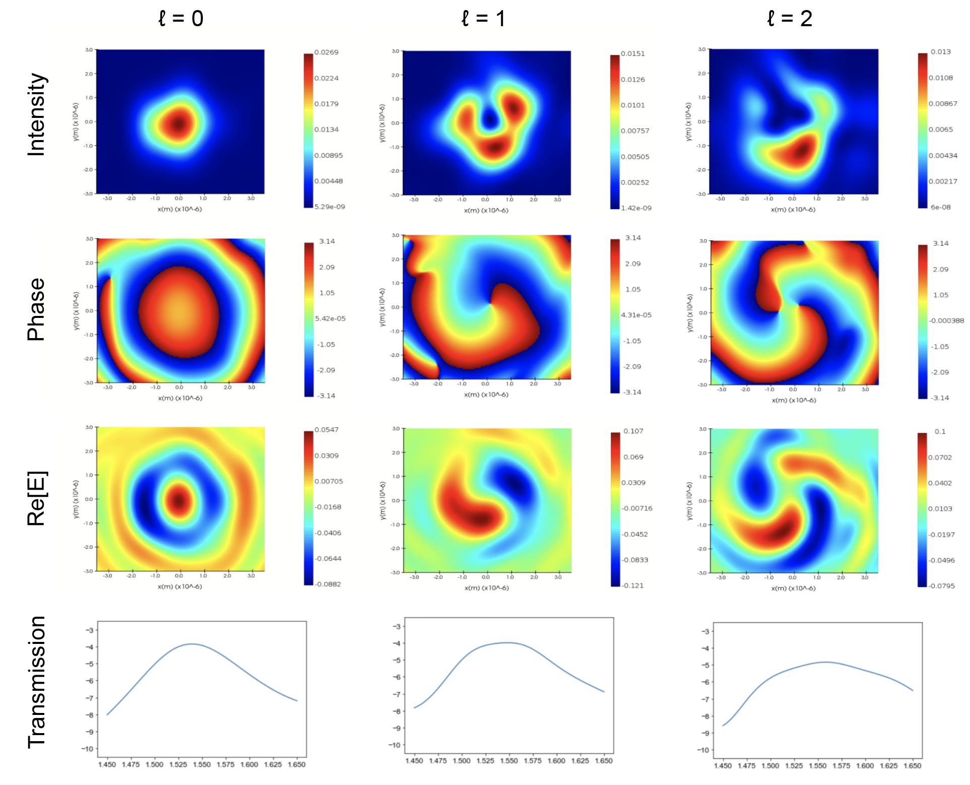
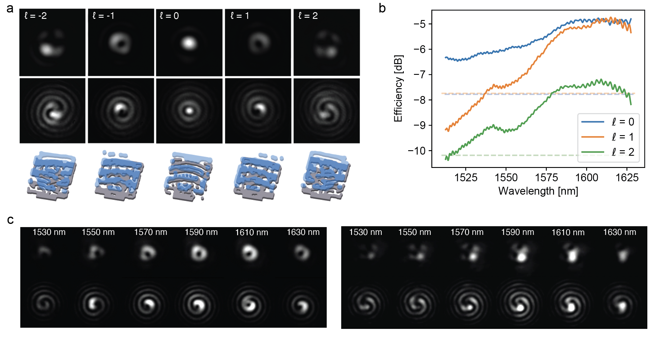
Finally, we utilize the well controlled fabrication and heterogeneous integration from the A*STAR AMF foundry to generate high fidelity, wide bandwidth and efficient vortex beam emitters. To do this, we implement an FDFD adjoint optimization package capable of the simultaneous optimization of multiple design regions Goos (2021). In combination with multilayer photonics processing Sacher et al. (2015), this allows us to design fully 3D structures parameterized by slices in the dimension. We design to devices consisting of two co-optimized layers; a 220 nm silicon layer with a 140 nm minimum feature size, and a 400 nm silicon nitride layer with a 300 nm minimum feature size. The layers are separated by 250 nm and are clad with silicon oxide.
The measured intensity and interference patterns of these devices is shown in Figure 4a (simulated results shown in Supplemental Figure 3). The additional degrees of freedom given by the 2 layer design, as well as the better controlled fabrication process of a foundry, allows us to see significant improvements in the beam shapes. Additionally, these emitters are able to maintain OAM emission across at least a 100 nm optical bandwidth (Figure 4b). To measure the emitter efficiency, we couple the to a multimode fiber that supports OAM beams and sweep the input wavelength and find that the 3dB bandwidths exceed 100 nm (Figure 4c).
We demonstrated a general optimization technique for beam emitters and applied it to generate optical vortex beams. We showed compact generation of to vortex beams, a vortex beam multiplexer, and high-performance foundry-fabricated heterogeneously-integrated multi-layer devices. The robustness of this approach in generating multiple orders and combinations of vortex beams and its ability to translate to foundry processing opens the door for applications in classical and quantum communications, information processing, and imaging.
Materials and Methods
Optimizations
Using adjoint optimization as described in Su et al. (2020), we maximize the free space overlap of OAM beams given a fundamental TE waveguide mode input. This maximization is defined as
where is the vectorized electric field due to the designed permitted distribution and c is the vectorized electric field of the desired OAM beam in free space. The devices in figures 2 and 3 were optimized for 1550 nm, and the devices in figure 4 were optimized for both 1530 nm and 1570 nm. The software to perform these optimization is publicly available at Goos (2021).
References
- Ni et al. (2021) J. Ni, C. Huang, L.-M. Zhou, M. Gu, Q. Song, Y. Kivshar, and C.-W. Qiu, Science 374, eabj0039 (2021).
- Shen et al. (2019) Y. Shen, X. Wang, Z. Xie, C. Min, X. Fu, Q. Liu, M. Gong, and X. Yuan, Light: Science & Applications 8, 1 (2019).
- Barreiro et al. (2008) J. T. Barreiro, T.-C. Wei, and P. G. Kwiat, Nature physics 4, 282 (2008).
- Wang et al. (2012) J. Wang, J.-Y. Yang, I. M. Fazal, N. Ahmed, Y. Yan, H. Huang, Y. Ren, Y. Yue, S. Dolinar, M. Tur, et al., Nature photonics 6, 488 (2012).
- Ren et al. (2016) H. Ren, X. Li, Q. Zhang, and M. Gu, Science 352, 805 (2016).
- Cai et al. (2012) X. Cai, J. Wang, M. J. Strain, B. Johnson-Morris, J. Zhu, M. Sorel, J. L. O’Brien, M. G. Thompson, and S. Yu, Science 338, 363 (2012).
- Miao et al. (2016) P. Miao, Z. Zhang, J. Sun, W. Walasik, S. Longhi, N. M. Litchinitser, and L. Feng, Science 353, 464 (2016).
- Liu et al. (2017) Q. Liu, Y. Zhao, M. Ding, W. Yao, X. Fan, and D. Shen, Optics Express 25, 23312 (2017).
- Kitamura et al. (2019) K. Kitamura, M. Kitazawa, and S. Noda, Optics Express 27, 1045 (2019).
- Bahari et al. (2021) B. Bahari, L. Hsu, S. H. Pan, D. Preece, A. Ndao, A. El Amili, Y. Fainman, and B. Kanté, Nature Physics 17, 700 (2021).
- Yu et al. (2011) N. Yu, P. Genevet, M. A. Kats, F. Aieta, J.-P. Tetienne, F. Capasso, and Z. Gaburro, science 334, 333 (2011).
- Chen et al. (2018) M. L. Chen, L. J. Jiang, and W. E. Sha, Applied Sciences 8, 362 (2018).
- Sedeh et al. (2020) H. B. Sedeh, M. M. Salary, and H. Mosallaei, Nanophotonics 9, 2957 (2020).
- Su et al. (2012) T. Su, R. P. Scott, S. S. Djordjevic, N. K. Fontaine, D. J. Geisler, X. Cai, and S. Yoo, Optics express 20, 9396 (2012).
- Zhou et al. (2019) N. Zhou, S. Zheng, X. Cao, Y. Zhao, S. Gao, Y. Zhu, M. He, X. Cai, and J. Wang, Science advances 5, eaau9593 (2019).
- Zhao and Fan (2020) Z. Zhao and S. Fan, Journal of Lightwave Technology 38, 4435 (2020).
- Xie et al. (2018) Z. Xie, T. Lei, F. Li, H. Qiu, Z. Zhang, H. Wang, C. Min, L. Du, Z. Li, and X. Yuan, Light: Science & Applications 7, 18001 (2018).
- Song et al. (2020) H. Song, Z. Zhao, R. Zhang, H. Song, H. Zhou, K. Pang, J. Du, L. Li, C. Liu, X. Su, et al., Optics Letters 45, 4144 (2020).
- White et al. (2021) A. White, K. Yang, and J. Vučković, in CLEO: Science and Innovations (Optical Society of America, 2021) pp. SM4C–2.
- Bauer et al. (2015) T. Bauer, P. Banzer, E. Karimi, S. Orlov, A. Rubano, L. Marrucci, E. Santamato, R. W. Boyd, and G. Leuchs, Science 347, 964 (2015).
- Goos (2021) Goos, https://github.com/stanfordnqp/spins-b (2021).
- Su et al. (2020) L. Su, D. Vercruysse, J. Skarda, N. V. Sapra, J. A. Petykiewicz, and J. Vučković, Applied Physics Reviews 7, 011407 (2020).
- Bozinovic et al. (2013) N. Bozinovic, Y. Yue, Y. Ren, M. Tur, P. Kristensen, H. Huang, A. E. Willner, and S. Ramachandran, Science 340, 1545 (2013).
- Sacher et al. (2015) W. D. Sacher, Y. Huang, G.-Q. Lo, and J. K. Poon, Journal of lightwave technology 33, 901 (2015).
Acknowledgments The authors thank Kasper Van Gasse and Rahul Trivedi for productive discussions, and thank Mohamad Idjadi and Firooz Aflatouni for assistance in foundry integration. This research is supported by the Air Force Office of Scientific Research (FA9550-17-1-0002), DARPA under the PIPES program, the Vannevar Bush Faculty Fellowship (N00014-19-1-2632), and ONR-MURI (N00014-20-1-2450).
Supplemental Information