Enhanced two-component superconductivity in CoSi2/TiSi2 heterojunctions
Abstract
We report enhanced two-component superconductivity in (CoSi2/Si)/TiSi2 superconductor/normal-metal (S/N) heterojunctions. An enhanced superconducting transition temperature about twice that of CoSi2 and an upper critical field 20 times bigger than that of epitaxial CoSi2/Si films were found. The tunneling spectra of three-terminal S/N junctions show pronounced zero-bias conductance peaks (ZBCPs) that signify penetration of odd-frequency, spin-triplet and even-parity Cooper pairs in TiSi2 from triplet dominant pairing in CoSi2/Si driven by symmetry reduction at the CoSi2/Si interface. Both the enhancement of value and the ZBCPs are found to be more pronounced if TiSi2 is made more diffusive.
The physics of novel quantum states of matter and in particular non-conventional superconducting states have been central of recent condensed matter research. This development is driven by scientific interest and technological prospects. Notably, the ability to engineer and manipulate entangled quantum states in dedicated devices holds promise for realizing topological quantum computation Read and Green (2000); Nayak et al. (2008); Qi and Zhang (2011); Alicea (2012). A major challenge is the identification of systems that incorporate both aspects of generation and manipulation of such quantum states at the microscopic scale. This involves the identification of non-trivial pairing states. A three terminal T-shaped proximity structure [Fig. 1(a)] had been proposed to aid distinguishing triplet from singlet superconductors (Asano et al., 2007). This T-shaped proximity structure detects triplet pairing through a zero-bias conductance peak (ZBCP) that results from the generation of odd-frequency spin-triplet even-parity pairs in the diffusive normal metal (DN) part of the superconductor/normal metal (S/N) interface Tanaka et al. (2005); *Tanaka2005_ERR; Tanaka and Golubov (2007). Yet, the fabrication of such T-shaped structures has proven difficult for many materials Courtois et al. (1999); Mackenzie et al. (2017). Moreover, interfaces and electronic confinement that appear to be inherent to such devices can also give rise to such intricate phenomena like interface superconductivity Pereiro et al. (2011).
The successful fabrication of high-quality CoSi2/TiSi2 T-shaped proximity structures on silicon was recently reported Chiu et al. (2021a, b). CoSi2 is a superconductor that is widely used in the semiconductor industry with a transition temperature () of K Matthias (1952); Matthias and Hulm (1953); Tsutsumi et al. (1997); Mattheiss and Hamann (1988). Interestingly, Chiu et al. established the existence of triplet pairing in these junctions via the anomalous proximity effect (APE) that leads to a ZBCP Chiu et al. (2021a). A possible way of understanding these findings in terms of the symmetry reduction brought about by the underlying dielectric substrate was proposed in Ref. Mishra et al. (2021). This is in line with the finding that the accompanying interface between CoSi2 and the Si(100) substrate Chiu et al. (2017) gives rise to a spin-orbit coupling (SOC) which exceeds the bulk CoSi2 superconducting energy gap by a factor 30 Chiu et al. (2021a). Therefore, parity no longer remains a good quantum number and that reflects in the gap structure , which is a combination of singlet and triplet components. is a matrix in spin-space, and is the -vector of the triplet pairing, denote the Pauli matrices, and is the identity matrix in spin-space. Highest is realized when the is along the SOC field Gor’kov and Rashba (2001); Frigeri et al. (2004), which is in the present case due to broken inversion symmetry along the axis. Here is the momentum vector.
In this Letter, we report superconductivity in CoSi2/TiSi2 heterostructures with an onset temperature () of roughly twice of . The presence of superconductivity in the junction is inferred through the APE. Our in-depth comparison with Ref. Mishra et al. (2021) indicates a mixture of singlet and triplet pairing channels with a dominant triplet component which drives the APE. A Ginzburg-Landau (GL) analysis is presented that captures the enhancement and provides a modeling of the system. Our analysis also sheds light on the roles played by the different interfaces forming the CoSi2/TiSi2 heterostructures.
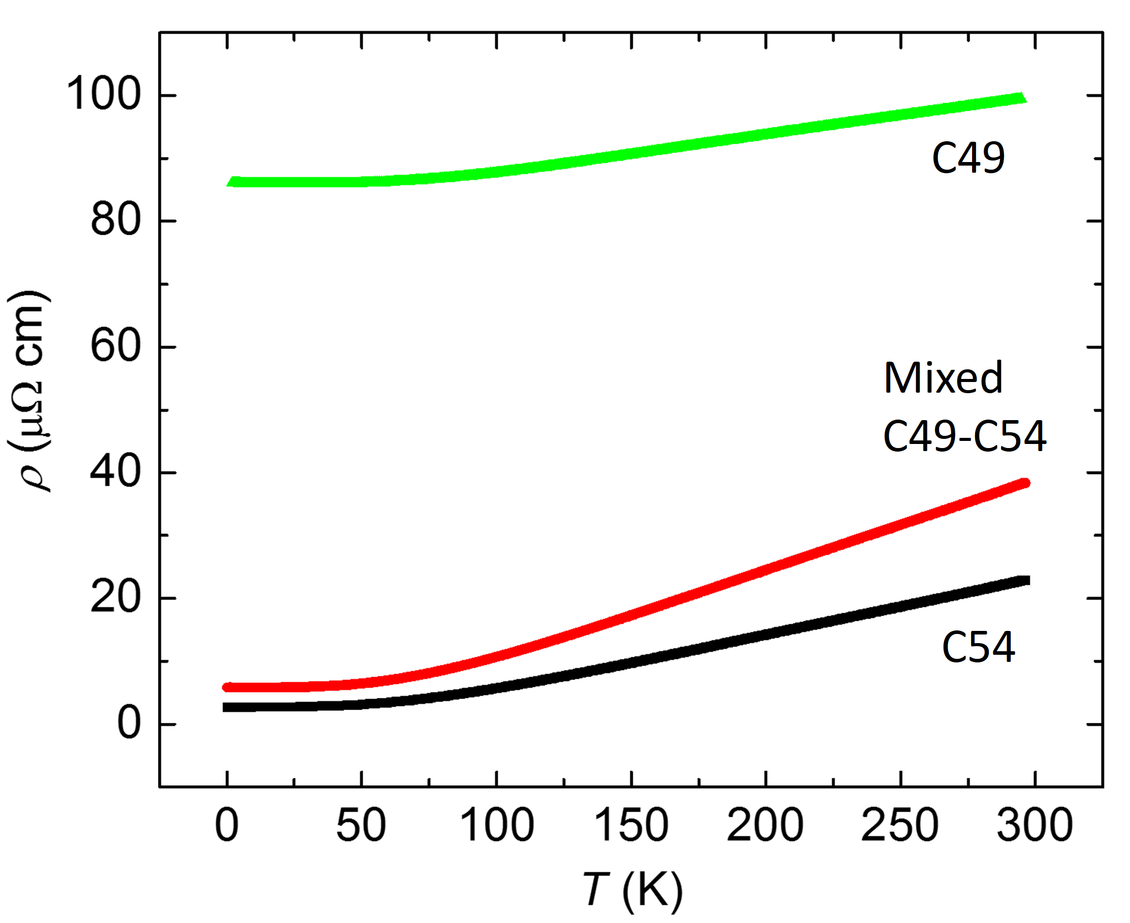
TiSi2 is a DN and remains metallic down to mK Chiu et al. (2021a). With respect to the CoSi2/TiSi2 proximity structures, it will be important that TiSi2 can exist in a base-centered phase (C49) and a face-centered phase (C54) Mattheiss and Hensel (1989); Ekman and Ozoliņš (1998). The C49 phase is known to contain large amounts of stacking faults Ma and Allen (1994). It has an order of magnitude larger resistivity [(300 K) (100–200) cm] than the C54 phase [(300 K) (17–25) cm] Sup . This inherent material property allows us to investigate the characteristics of the CoSi2/TiSi2 proximity structure in terms of the diffusive properties of the normal-metal component.
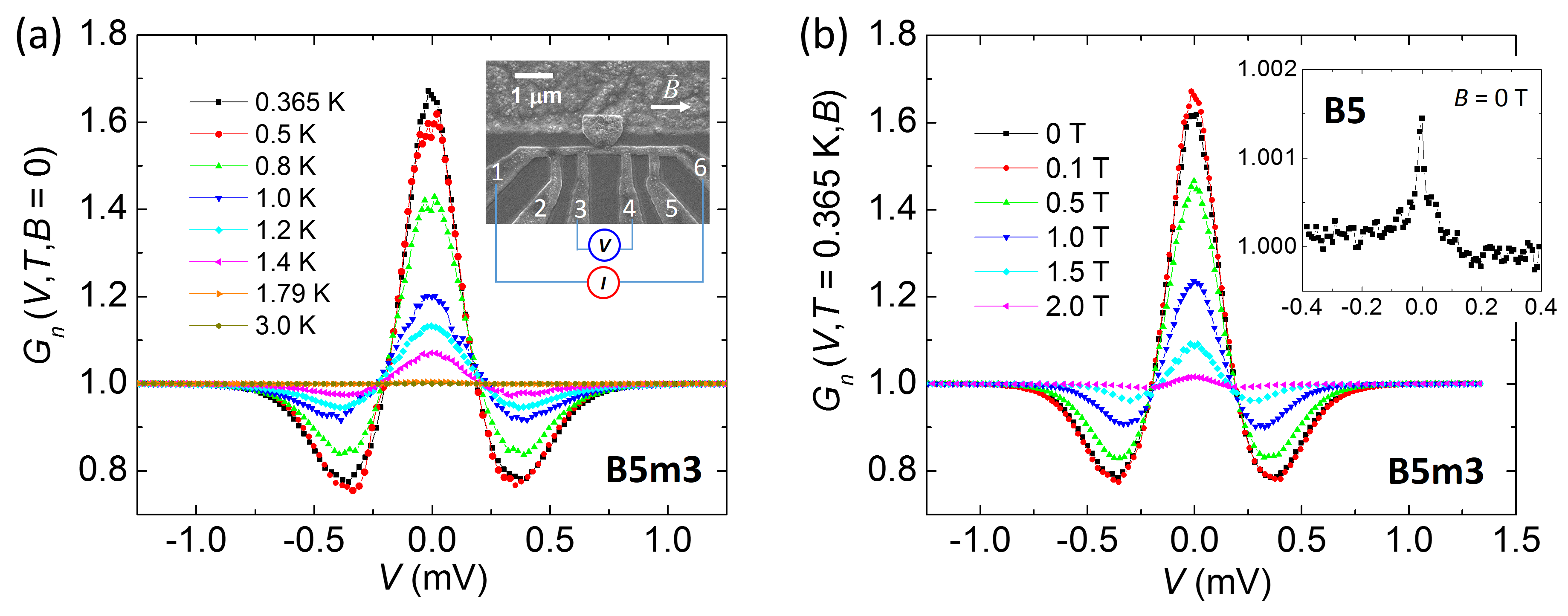
Surprisingly, in a number of devices, is significantly enhanced ( K). The enhanced value is not only higher than those in the T-shaped structures studied in Ref. Chiu et al. (2021a) ( K), but also higher than the value ( 1.5 K) of epitaxial CoSi2/Si films Chiu et al. (2017). Moreover, the normalized amplitude of ZBCP is strongly enhanced up to 210% with respect to the (normalized) conductance of the normal state. In Fig. 1(a), the inset depicts a schematic T-shaped structure with a 4-probe configuration for measuring the proximity effect in TiSi2, which is 125-nm thick and typically (0.30.1)-m wide. (The thickness of the CoSi2/Si films is 105 nm in this work.) The main panel shows the normalized zero-bias conductance as a function of for six devices, where denotes the differential conductance, , normalized to its normal-state value, where is the current, is the bias voltage, is the temperature, and is the magnetic field.
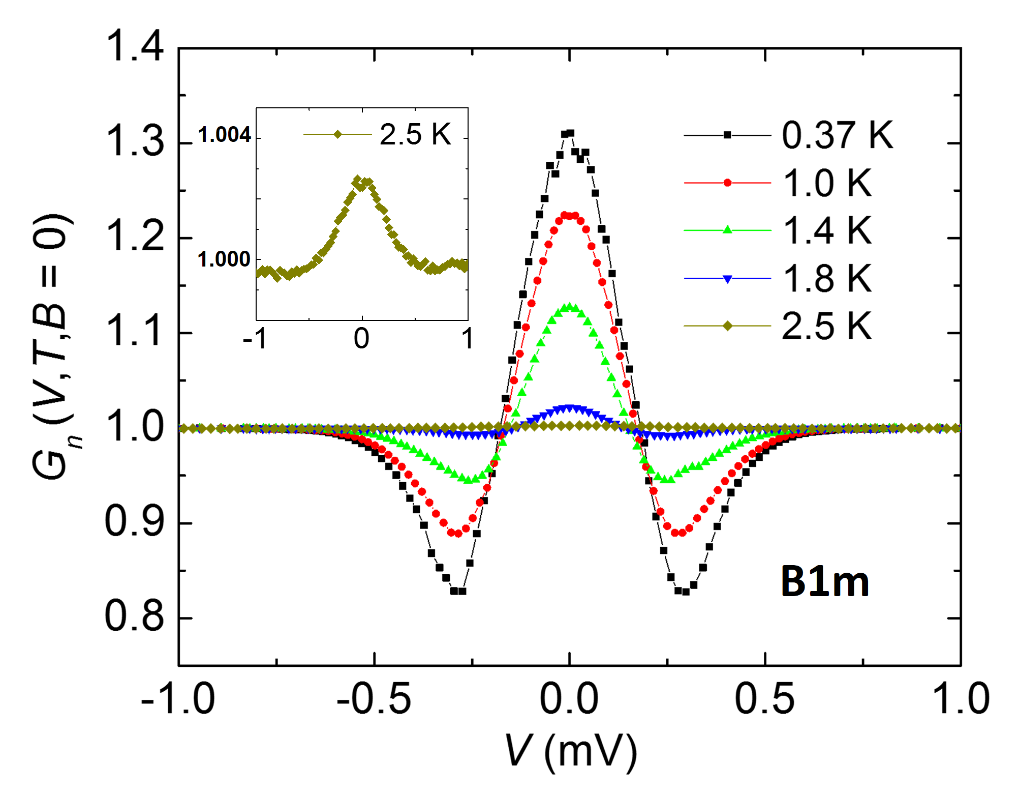
In Fig. 1(a), devices B1, B2, B3 and B5 were measured as grown. Device B1 (B5) then underwent one (three) thermal cycling to room temperature and cooled down again for a second- (fourth-)run measurement [the device is subsequently relabeled B1m (B5m3)] Sup . The of device B1 (B1m) increases with decreasing below an onset temperature K (2.84 K), reaching 212% (131%) at 0.365 K. There are visible conductance fluctuations which are probably induced by dynamical structural defects in this particular device Yeh et al. (2017). The in device B2 shows a non-monotonic dependence, increasing below 2.33 K and reaching a maximum at 0.75 K, then followed by a small decrease to 110% at 0.37 K. The in device B3 shows a monotonic increase below 2.14 K, reaching 106% at 0.37 K. of device B5 is relatively small compared to that of device B5m3. Figure 1(a) demonstrates that the magnitude of the APE is strongly influenced by the high resistivity, i.e., low electron diffusivity, of the C49 phase.
Figure 1(b) depicts the of device B1 in several fields. In this work, the field was applied in the CoSi2/Si plane and parallel to the S/N interface. The is gradually suppressed with increasing but a small proximity effect is still visible in T which is much higher than the in-plane upper critical field ( T) of CoSi2/Si films Chiu et al. (2021a). Figure 1(c) depicts of the same device at several values and in . ZBCPs are notable, which are gradually suppressed with increasing . The ZBCP persists up to at least 2.5 K (see a zoom-in in the inset). Figure 1(d) shows of the same device in several fields and at K. While the ZBCP is gradually suppressed with increasing , it persists up to at least 2 T (Fig. 1d inset).
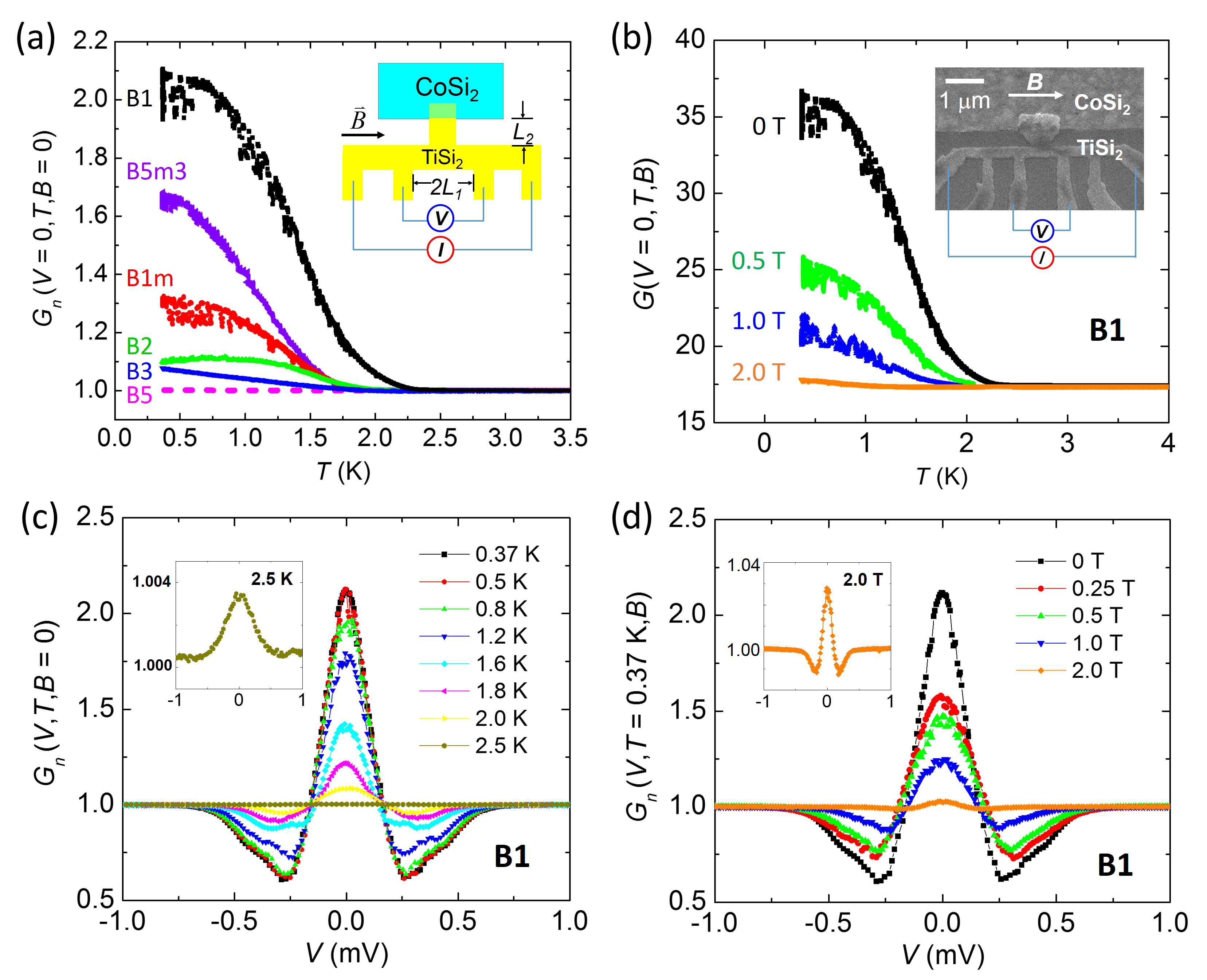
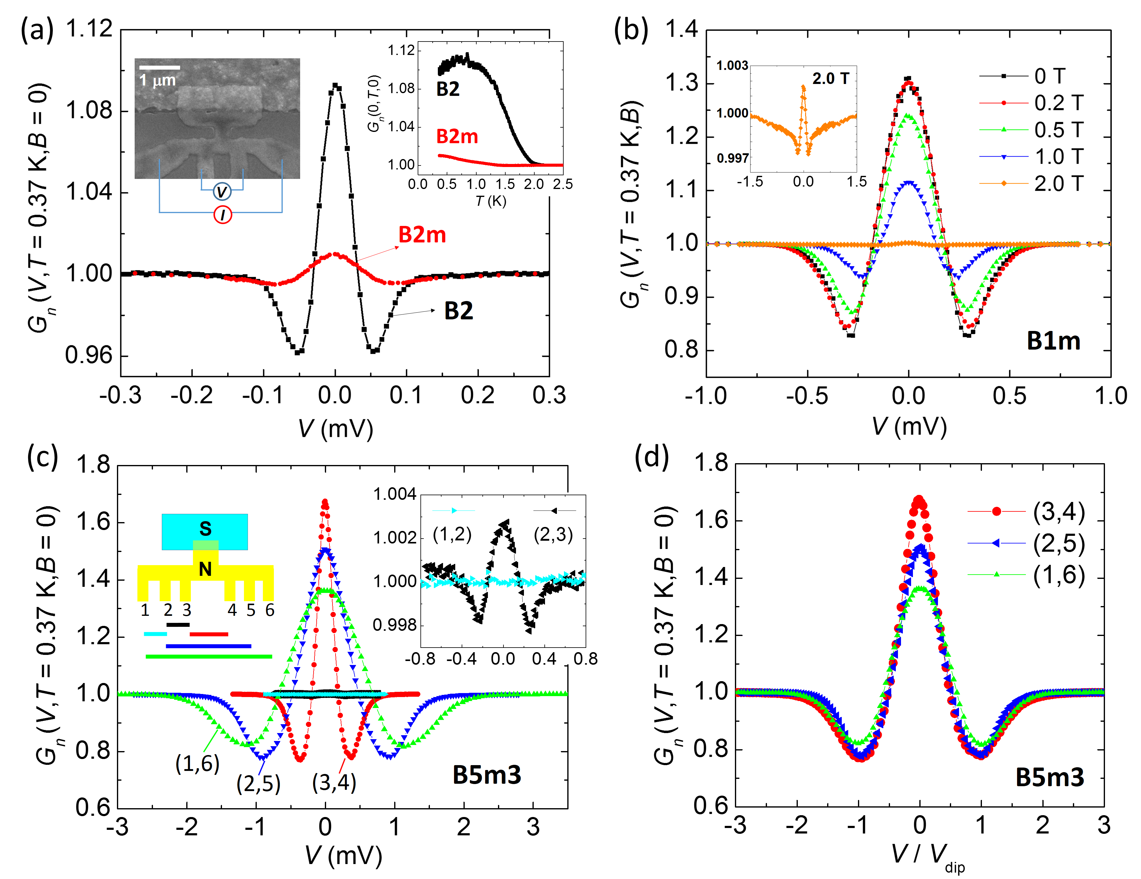
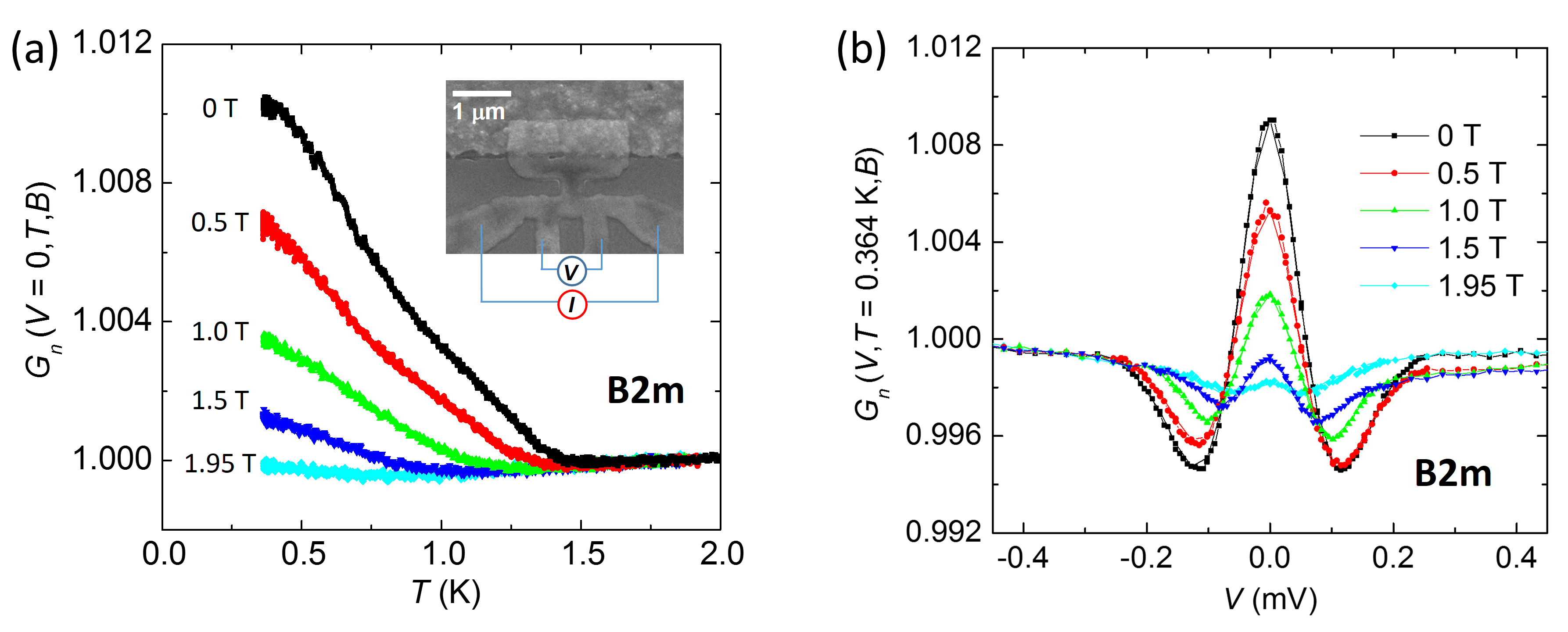
To test the robustness of the ZBCPs and the effect of thermal cycling on the APE, Fig. 2(a) shows the of B2 and B2m at K and in = 0. (B2m denotes the second-run measurement of B2). The amplitude of ZBCP of B2m is notably reduced from that of B2. Nevertheless, it remains readily detectable. The right inset shows that the in is reduced from 2.33 K in B2 to 1.42 K in B2m.
We use device B1m to demonstrate that the APE persists up to large fields. Figure 2(b) shows of device B1m in several fields and at K. Although the amplitudes are smaller compared with those in Fig. 1(d), the ZBCPs are robust against thermal cycling. The inset shows a zoom-in for the 2.0-T curve, where the ZBCP is still not completely suppressed.
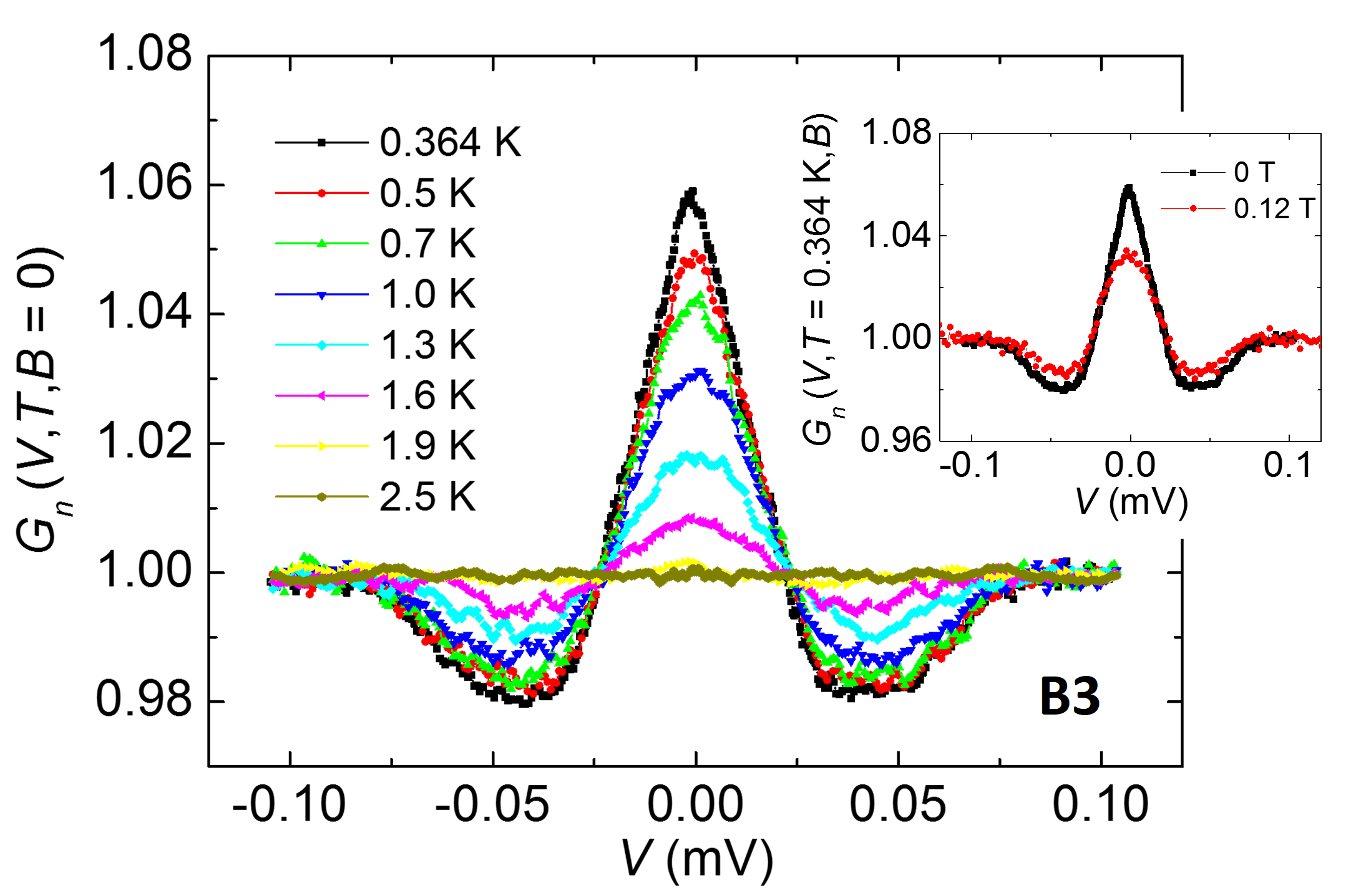
Thus, the superconductivity enhancement is robust and closely correlated with the diffusivity of TiSi2. We have thermally cycled device B5 three times to further investigate the APE. In addition, we use this device to illustrate that the ZBCPs only occur in the vicinity of the CoSi2/TiSi2 interface. The left inset of Fig. 2(c) shows a schematic S/N T-shaped device with six submicron electrodes attaching N. The main panel of Fig. 2(c) shows the for different voltage-electrode (VE) pairs which define different segments of the TiSi2 component. In all cases, was applied through the outermost electrode pair (1,6). Figure 2(c) reveals large amplitudes of ZBCP measured with the VE pairs (3,4), (2,5) and (1,6). In contrast, the right inset shows a zoom-in of the small ZBCPs for the VE pairs (1,2) and (2,3), located away from the S/N interface. In fact, the curve for the VE pair (1,2) is flat, indicating a complete absence of the APE. These results provide unambiguous evidence that the ZBCP must arise from the penetration of Cooper pairs through the CoSi2/TiSi2 interface, as theoretically predicted for triplet superconductivity Asano et al. (2007).
Figure 2(d) shows for VE pairs (3,4), (2,5) and (1,6) vs. , where are the voltages where the two side dips occur in each VE pair configuration. The lineshapes of all three curves are similar, while the amplitudes of ZBCP decrease with increasing VE pair separation, as expected. When the VE pair separation is large, no Cooper pairs can diffuse to those TiSi2 regimes far away from the S/N interface. Thus, those TiSi2 regimes contribute a finite resistance, leading to a reduced ZBCP height.
We apply a quasi-classical description of the CoSi2/TiSi2 three-terminal heterojunctions Asano et al. (2007); Mishra et al. (2021) and consider a SOC induced pairing state with a dominant triplet component Mishra et al. (2021). Within the formulation of the circuit theory Nazarov (1999); Tanaka et al. (2003, 2004a); *Tanaka2004_ERR, an insulating barrier is expressed as a delta function [] at the S/N interface. The weight of the barrier is expressed in terms of a dimensionless parameter , Fermi energy , and the Fermi wavenumber . A higher ratio of , i.e., resistance of the normal-metal component () over barrier resistance (), results in an APE over a broader energy range and thus in an increase in the FWHM of the ZBCP Asano et al. (2007). The zero-bias value itself, however, is (roughly) independent of / if electron dephasing is ignored in the DN component of the junction.
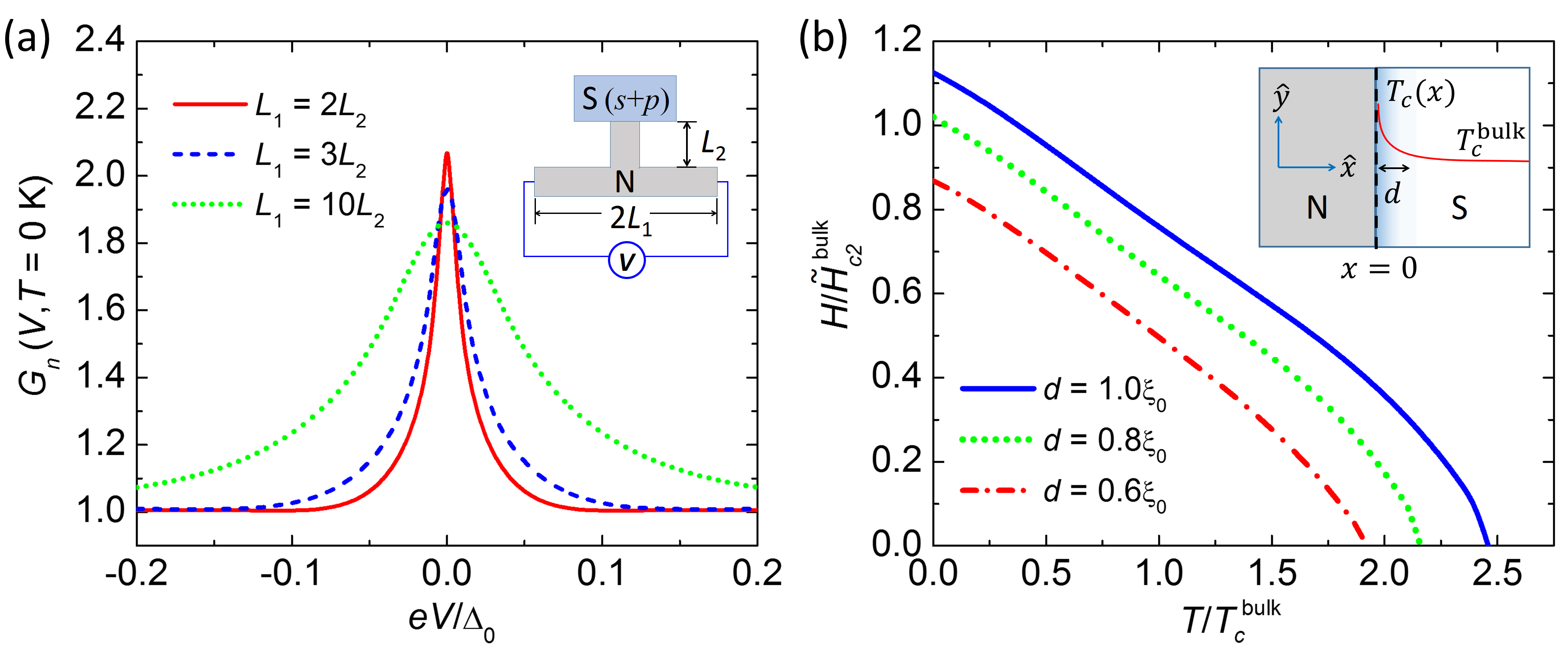
In Fig. 3(a), we keep , , and fixed, and vary according to the experiments as shown in Fig. 2(c). Importantly, when VE configuration is changed, the S/N interface properties remain fixed but as changes changes likewise. We find that the ZBCP becomes broader, in qualitative agreement with Fig. 2(c). While this variation of FWHM with agrees with the experiment, the inclusion of a small amount of electron dephasing is required to reproduce the experimental behavior of , i.e., a suppression of with increasing . In diffusive metals, the existence of a finite electron dephasing rate in low- regimes have been reported for long, but its microscopic origin(s) are yet to be fully identified Lin and Bird (2002). Magnetic impurities as a source of dephasing however appears unlikely as their presence in the heterojunction has been ruled out Chiu et al. (2021a). For the C49 phase, is higher than in the C54 phase, which results in a larger ZBCP provided other parameters are kept constant. Across the devices, the behavior of ZBCP can be interpreted along this line, but typically, several device parameters undergo changes from device to device or upon thermal cycling (section C of Sup ). Nevertheless, the robust ZBCPs in these devices support the interpretation in terms of the SOC generated two-component superconductivity with a dominant triplet component, which is essential for the ZBCP.
The enhanced is usually found in T-shaped structures with high- TiSi2. This leads to the important observation that when (TiSi2) is reduced by thermal cycling, the enhancement of superconductivity is also reduced, i.e., the enhanced superconductivity is correlated with some kind of defect structures. The case of B5 (and B5m3) further supports this conclusion because after thermal cycling B5m3 became more resistive and enhanced superconductivity emerged.
The quasi-classical theory provides a good explanation for the robustness of the ZBCPs in T-shaped junctions, but does not take into account the enhanced superconductivity found in these devices. As the interface quality plays a vital role in the enhancement of superconductivity, we will assume that somewhere near or at the S/N interface there exists another superconducting phase whose is higher than . Its microscopic origin could be changes in the electronic structure or changes in the phonon modes, as in YIr2-Ir and EuIr2-Ir eutectic systems Matthias et al. (1980); Suhl et al. (1980). Here we focus on a phenomenological description of this effect rather than a microscopic modeling.
We adopt GL theory for the singlet-triplet mixed superconducting state to understand this phenomena. The free energy for such a system reads Sigrist (2009),
| (1) |
here is the usual GL free energy for each individual component, the subscript represents the two components of the order parameter, and is , where is the vector potential, and is the magnetic flux quantum. The coefficient is . We assume a clean superconductor and . is the coupling between the two components, a negative value of the coefficient ensures a single transition temperature and is the free energy density of the non-superconducting state without magnetic field (). is the contribution from the magnetic field 111 denotes the total magnetic field. refers to the external field as common in the GL literature. has to be identified with of Figs. 1 and 2.. is a Lifshitz invariant term that leads to a magneto-electric coupling and determines the effect of superconducting order on spin-polarization, where labels spatial components.
We take the S/N interface at and assume a homogeneous system along the other directions. We restrict ourselves to the experimental field configuration, i.e., along the interface in the plane (). The coefficients of the quadratic terms are taken to be spatially varying to model the enhanced superconductivity near the interface. This dependence of is , where and and are dimensionless parameters determining the amount of enhancement. is the width of the effective interface. A similar model was adopted previously to model the 3-K phase Maeno et al. (1998); Ando et al. (1999); Mao et al. (2001); Wang et al. (2017) of Sr2RuO4 Sigrist and Monien (2001); Kaneyasu et al. (2019). The instability condition is obtained by minimizing the free energy. At the S/N interface we apply the De Gennes’s boundary conditions De Gennes (1964), where the extrapolation length is a characteristic length scale associated with the induced superconducting correlations. In contrast to conventional superconductors, here cannot be identified with the superconducting correlation length of the DN segment, because it does not account for the physics of odd-frequency pairs Tanaka and Golubov (2007); Tanaka et al. (2012); Linder and Balatsky (2019). We therefore treat as a phenomenological parameter.
Figure 3(b) illustrates the vs. phase diagram for the appearance of onset order at the interface for various values. The onset temperature and magnetic field are obtained by minimizing the free energy, Eq. (1), with De Gennes’s boundary conditions with extrapolation , where is the coherence length at for the bulk superconductor, see also S1 ofSup . Within the GL formalism, exceeds in the low-field limit, and the decreases with increasing field. In our calculations, we find that the onset magnetic field in the low- limit is comparable to , which is a magnetic field scale of the order of orbital upper critical fields. However, quantitatively the onset magnetic field is much smaller compared to the experiments, despite a reasonable obtained from theoretical calculations.
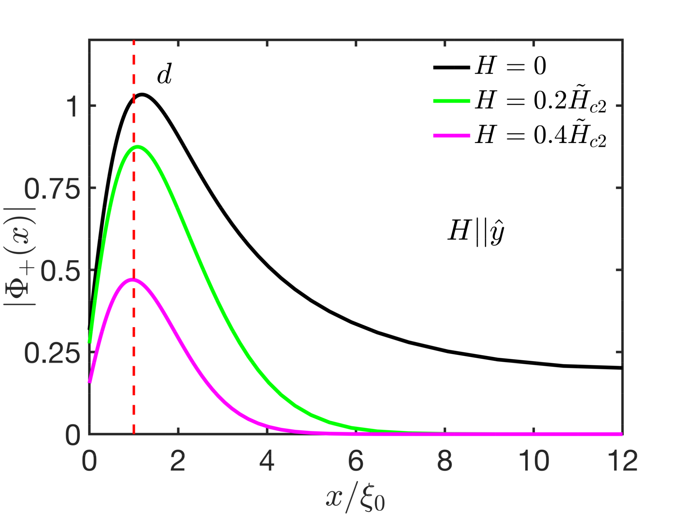
In the low limit, the onset magnetic field exceeds the upper critical field of the bulk superconductor by a factor 100 Matthias and Hulm (1953) and that of CoSi2/Si films by 20 Chiu et al. (2021a). The experimental onset magnetic field is above 2 T and this value is comparable to the Pauli-limited field for the bulk superconductor ( 2.4 T). The GL theory does not include the effect of Pauli paramagnetism or possible finite momentum pairing, suggesting that this could be the origin of the quantitative disagreement between the theory and experiment. The interface induced order survives up to 10–12 coherence lengths from the surface Sup . As shown in the Fig. 3(b), for the appearance of such order above is very sensitive to the width of the interface. As the interface region becomes thinner, drops rapidly. In the devices with C49 phase, the interface region is expected to be relatively more disordered and its effective width is expected to be high compared to the low- devices, due to smaller grain sizes or possible incomplete C49-C54 transformation (see S3 of Sup, ).
Thus, Eq. (1) provides an effective model for the CoSi2/TiSi2 heterojunctions. The term which suggest that the (CoSi2/Si)/TiSi2 system is an ideal system to explore e.g. the superconducting diode effect and charge transport effects Ando et al. (2020); Wakatsuki et al. (2017). Our results also demonstrate the stability of the APE, and the prevalence of odd-frequency pairing in heterostructures Tanaka and Golubov (2007); Tanaka et al. (2012); Linder and Balatsky (2019)
In conclusion, we have shown that the CoSi2/TiSi2 T-shaped proximity devices show strong evidence for two-component superconductivity. The tunneling spectra are robust against disorder, and the onset temperature for this two-component superconducting state exceeds the bulk with enhanced disorder. The large SOC which drives the two-component superconductivity is a result of the symmetry reduction due to the CoSi2/Si(100) interface, while the enhancement is driven by the CoSi2/TiSi2 interface. We use quasi-classical theory to understand the tunneling spectra and a phenomenological theory to understand the enhanced superconductivity. The microscopic origin of this enhancement and the zero-bias conductance lineshape is left for future studies.
Acknowledgements.
Acknowledgments – We thank S. S. Yeh for experimental help. This work was supported by the Ministry of Science and Technology of Taiwan through grant numbers MOST 106-2112-M-009-007-MY4 and 110-2112-M-A49-015, and by the Ministry of Education of Taiwan through the Higher Education Sprout Project. VM, YL and FCZ are partially supported by NSFC grants 11674278 and 11920101005 and by the priority program of the Chinese Academy of Sciences grant No. XDB28000000, and by the China Postdoctoral Science Foundation under grant No. 2020M670422 (YL).References
- Read and Green (2000) N. Read and D. Green, Phys. Rev. B 61, 10267 (2000).
- Nayak et al. (2008) C. Nayak, S. H. Simon, A. Stern, M. Freedman, and S. Das Sarma, Rev. Mod. Phys. 80, 1083 (2008).
- Qi and Zhang (2011) X.-L. Qi and S.-C. Zhang, Rev. Mod. Phys. 83, 1057 (2011).
- Alicea (2012) J. Alicea, Reports on Progress in Physics 75, 076501 (2012).
- Asano et al. (2007) Y. Asano, Y. Tanaka, A. A. Golubov, and S. Kashiwaya, Phys. Rev. Lett. 99, 067005 (2007).
- Tanaka et al. (2005) Y. Tanaka, Y. Asano, A. A. Golubov, and S. Kashiwaya, Phys. Rev. B 72, 140503 (2005).
- Tanaka et al. (2006) Y. Tanaka, Y. Asano, A. A. Golubov, and S. Kashiwaya, Phys. Rev. B 73, 059901 (2006).
- Tanaka and Golubov (2007) Y. Tanaka and A. A. Golubov, Phys. Rev. Lett. 98, 037003 (2007).
- Courtois et al. (1999) H. Courtois, P. Charlat, P. Gandit, D. Mailly, and B. Pannetier, Journal of Low Temperature Physics 116, 187 (1999).
- Mackenzie et al. (2017) A. P. Mackenzie, T. Scaffidi, C. W. Hicks, and Y. Maeno, npj Quantum Materials 2, 40 (2017).
- Pereiro et al. (2011) J. Pereiro, A. Petrovic, C. Panagopoulos, and I. Božović, “Interface superconductivity: History, development and prospects,” (2011), arXiv:1111.4194 .
- Chiu et al. (2021a) S.-P. Chiu, C. C. Tsuei, S.-S. Yeh, F.-C. Zhang, S. Kirchner, and J.-J. Lin, Science Advances 7, eabg6569 (2021a).
- Chiu et al. (2021b) S.-P. Chiu, W.-L. Lai, and J.-J. Lin, Japanese Journal of Applied Physics 60, 088002 (2021b).
- Matthias (1952) B. T. Matthias, Phys. Rev. 87, 380 (1952).
- Matthias and Hulm (1953) B. T. Matthias and J. K. Hulm, Phys. Rev. 89, 439 (1953).
- Tsutsumi et al. (1997) K. Tsutsumi, S. Takayanagi, and T. Hirano, Physica B: Condensed Matter 237-238, 310 (1997).
- Mattheiss and Hamann (1988) L. F. Mattheiss and D. R. Hamann, Phys. Rev. B 37, 10623 (1988).
- Mishra et al. (2021) V. Mishra, Y. Li, F.-C. Zhang, and S. Kirchner, Phys. Rev. B 103, 184505 (2021).
- Chiu et al. (2017) S.-P. Chiu, S.-S. Yeh, C.-J. Chiou, Y.-C. Chou, J.-J. Lin, and C.-C. Tsuei, ACS Nano 11, 516 (2017).
- Gor’kov and Rashba (2001) L. P. Gor’kov and E. I. Rashba, Phys. Rev. Lett. 87, 037004 (2001).
- Frigeri et al. (2004) P. A. Frigeri, D. F. Agterberg, A. Koga, and M. Sigrist, Phys. Rev. Lett. 92, 097001 (2004).
- Mattheiss and Hensel (1989) L. F. Mattheiss and J. C. Hensel, Phys. Rev. B 39, 7754 (1989).
- Ekman and Ozoliņš (1998) M. Ekman and V. Ozoliņš, Phys. Rev. B 57, 4419 (1998).
- Ma and Allen (1994) Z. Ma and L. H. Allen, Phys. Rev. B 49, 13501 (1994).
- (25) see Supplemental Material.
- Yeh et al. (2017) S.-S. Yeh, W.-Y. Chang, and J.-J. Lin, Science Advances 3, e1700135 (2017).
- Nazarov (1999) Y. V. Nazarov, Superlattices and Microstructures 25, 1221 (1999).
- Tanaka et al. (2003) Y. Tanaka, Y. V. Nazarov, and S. Kashiwaya, Phys. Rev. Lett. 90, 167003 (2003).
- Tanaka et al. (2004a) Y. Tanaka, Y. V. Nazarov, A. A. Golubov, and S. Kashiwaya, Phys. Rev. B 69, 144519 (2004a).
- Tanaka et al. (2004b) Y. Tanaka, Y. V. Nazarov, A. A. Golubov, and S. Kashiwaya, Phys. Rev. B 70, 219907 (2004b).
- Lin and Bird (2002) J. J. Lin and J. P. Bird, Journal of Physics: Condensed Matter 14, R501 (2002).
- Matthias et al. (1980) B. T. Matthias, G. R. Stewart, A. L. Giorgi, J. L. Smith, Z. Fisk, and H. Barz, Science 208, 401 (1980).
- Suhl et al. (1980) H. Suhl, B. T. Matthias, S. Hecker, and J. L. Smith, Phys. Rev. Lett. 45, 1707 (1980).
- Sigrist (2009) M. Sigrist, AIP Conference Proceedings 1162, 55 (2009).
- Note (1) denotes the total magnetic field while refers to the external field as is common in the GL literature. has to be identified with of Figs. 1 and 2.
- Maeno et al. (1998) Y. Maeno, T. Ando, Y. Mori, E. Ohmichi, S. Ikeda, S. NishiZaki, and S. Nakatsuji, Phys. Rev. Lett. 81, 3765 (1998).
- Ando et al. (1999) T. Ando, T. Akima, Y. Mori, and Y. Maeno, Journal of the Physical Society of Japan 68, 1651 (1999).
- Mao et al. (2001) Z. Q. Mao, K. D. Nelson, R. Jin, Y. Liu, and Y. Maeno, Phys. Rev. Lett. 87, 037003 (2001).
- Wang et al. (2017) H. Wang, J. Luo, W. Lou, J. E. Ortmann, Z. Q. Mao, Y. Liu, and J. Wei, New Journal of Physics 19, 053001 (2017).
- Sigrist and Monien (2001) M. Sigrist and H. Monien, Journal of the Physical Society of Japan 70, 2409 (2001).
- Kaneyasu et al. (2019) H. Kaneyasu, Y. Enokida, T. Nomura, Y. Hasegawa, T. Sakai, and M. Sigrist, Phys. Rev. B 100, 214501 (2019).
- De Gennes (1964) P. G. De Gennes, Rev. Mod. Phys. 36, 225 (1964).
- Tanaka et al. (2012) Y. Tanaka, M. Sato, and N. Nagaosa, Journal of the Physical Society of Japan 81, 011013 (2012).
- Linder and Balatsky (2019) J. Linder and A. V. Balatsky, Rev. Mod. Phys. 91, 045005 (2019).
- Ando et al. (2020) F. Ando, Y. Miyasaka, T. Li, J. Ishizuka, T. Arakawa, Y. Shiota, T. Moriyama, Y. Yanase, and T. Ono, Nature 584, 373–376 (2020).
- Wakatsuki et al. (2017) R. Wakatsuki, Y. Saito, S. Hoshino, Y. M. Itahashi, T. Ideue, M. Ezawa, Y. Iwasa, and N. Nagaosa, Science Advances 3, e1602390 (2017).
— Supplemental Material —
Enhanced two-component superconductivity in CoSi2/TiSi2 heterojunctions
Shao-Pin Chiu,1,2,∗ Vivek Mishra,3,∗ Yu Li,3 Fu-Chun Zhang,3,4,5 Stefan Kirchner,1,2
and Juhn-Jong Lin1,2
1Department of Electrophysics, National Yang Ming Chiao Tung University, Hsinchu 30010, Taiwan
2Center for Emergent Functional Matter Science, NYCU, Hsinchu 30010, Taiwan
3Kavli Institute for Theoretical Sciences, University of Chinese Academy of Sciences, Beijing 100190, China
4CAS Center for Excellence in Topological Quantum Computation, University of Chinese Academy of Sciences, Beijing 100190, China
5HKU-UCAS Joint Institute of Theoretical and Computational Physics at Beijing, University of Chinese Academy of Sciences, Beijing 100190, China
- Summary
-
Below we provide additional technical details, further experimental data and auxiliary numerical results supplementing the conclusions from the main text.
A Ginzburg-Landau analysis of the enhanced interface two-component superconductivity
To find the ground state, we minimize the Ginzburg-Landau (GL) free energy, which results in,
| (I) | |||||
| (II) | |||||
Here , where is the magnetic flux quanta, and we set the vector potential , which gives the magnetic field in the direction. All lengths can be expressed in terms of the coherence length , where the coefficient is , is the average Fermi velocity, and is the density of states. Here refers to the bulk transition temperature. We assume an isotropic Fermi-surface and ignore the difference in the Fermi velocities and density of states of two helical bands formed due to the spin-orbit coupling. Similarly, the magnetic field can be measured in unit of , which is and all energies in these equations can be expressed in units of . The coefficient is . The coefficient is,
| (III) |
where is the Bohr magneton. The magneto-electric coefficient has opposite sign for two helical bands Sigrist (2009), and it reads,
| (IV) |
We further assume . Equations (I) and (II) are solved with De Gennes’s boundary condition at the superconductor and normal interface. Figure S1 shows the solution for various values of the magnetic field, and it shows that the order parameters remain finite up to several coherence lengths from the S/N interface.
B Additional Experimental Data
Auxiliary experimental data on the electrical-transport properties of normal-metal TiSi2 films (Fig. S2), as well as additional conductance spectra of CoSi2/TiSi2 T-shaped superconducting proximity structures (Figs. S3 to S6) are presented. A brief discussion of the data is provided in each of the figure captions.
C Device Characterizations
This supplemental section provides a compilation of the device parameters for the CoSi2/TiSi2 T-shaped proximity structures discussed in the main text.
Formation of C49 and C54 TiSi2 phases. Titanium films were deposited on an electron-beam lithographically patterned Si(100) substrate, and subsequently thermally annealed to form the normal-metal TiSi2 component in the T-shaped proximity structure. The phase formation sequence of titanium silicide followed the reaction path as the thermal annealing temperature was raised: Ti/Si amorphous TiSix polycrystalline C49 TiSi2 polycrystalline C54 TiSi2 Ma et al. (1991); Chen (2004). The C49 (C54) TiSi2 phase was obtained by annealing at 750∘C (800∘C) for about 1 h Chiu et al. (2021). A mixed C49-C54 TiSi2 phase could also be obtained by applying an intermediate annealing temperature 780∘C. Cross-sectional transmission electron microscopy studies revealed that the C49 phase had a smaller grain size ( 50–300 nm), compared with that ( 300–1000 nm) of the C54 phase. Moreover, the carrier concentration in the C49 phase ( 1.5 cm-3) is more than one order of magnitude lower than that ( 3 cm-3) in the C54 phase Mammoliti et al. (2002). Thus, (C49) (C54).
Thermal cycling effect and device labeling. After the conductance spectra of the as-grown device B1 (B2) were measured at low temperatures, the device was warmed up from 0.36 K to 300 K and cooled down again for a second-run measurement of the conductance spectra. The device was then labeled B1m (B2m), because the device properties (e.g., the transparency of the S/N interface as well as the defect configurations of the TiSi2 component) were often sensitive to thermal cycling and repeated finite-bias measurements. Device B5 was intentionally subject to three times of thermal cycling to check the robustness and reproducibility of the conductance spectra. Thus, B5m3 denotes the fourth-run measurement of device B5.
In the course of this study, we find that thermal cycling from liquid-helium temperature to 300 K could result in modifications of the CoSi2/TiSi2 interface and/or rearrangements of defect configurations in the TiSi2 component. We found that thermal cycling often caused a decrease in (TiSi2), but occasionally it resulted in an increase in (TiSi2). Moreover, we have observed that an enhanced value is more frequently found in those T-shaped structures made of high- TiSi2 component. In other words, in those T-shaped structures whose (TiSi2) values were reduced by thermal cycling, their values were also reduced.
| \rowcolorgray!50 Device | (∘C) | (m) | (m) | () | ( cm) | (at 0.37 K) | FWHM (meV) | (meV) | (cm2/s) | (K) |
|---|---|---|---|---|---|---|---|---|---|---|
| B1 | 750 | 0.42 | 0.39 | 57.5 | 197 | 112% | 0.18 | 0.0012 | 3.1 | 2.94 |
| B1m | 750 | 0.42 | 0.39 | 55.8 | 191 | 31% | 0.22 | 0.0012 | 3.2 | 2.84 |
| B2 | 750 | 0.20 | 0.66 | 12.0 | 79.8 | 9.3% | 0.04 | 0.013 | 7.7 | 2.33 |
| B2m | 750 | 0.20 | 0.66 | 12.7 | 84.3 | 1.0% | 0.056 | 0.012 | 7.3 | 1.42 |
| B3 | 780 | 0.23 | 0.10 | 0.346 | 2.14 | 5.9% | 0.026 | 0.13 | 106 | 2.14 |
| B5 | 800 | 0.45 | 0.32 | 1.31 | 3.34 | 0.13% | 0.03 | 0.023 | 67.9 | 1.50 |
| B5m3 | 800 | 0.45 | 0.32 | 19.1 | 48.6 | 66% | 0.20 | 0.004 | 12.7 | 2.10 |
References
- Sigrist (2009) M. Sigrist, AIP Conference Proceedings 1162, 55 (2009).
- Ma et al. (1991) Z. Ma, L. H. Allen, and S. Lee, MRS Proceedings 237, 661 (1991).
- Chen (2004) L. J. Chen, Silicide Technology for Integrated Circuits, EMIS Processing Series (The Institution of Engineering and Technology, 2004).
- Chiu et al. (2021) S.-P. Chiu, C. C. Tsuei, S.-S. Yeh, F.-C. Zhang, S. Kirchner, and J.-J. Lin, Science Advances 7, eabg6569 (2021).
- Mammoliti et al. (2002) F. Mammoliti, M. G. Grimaldi, and F. La Via, J. Appl. Phys. 92, 3147 (2002).