pcba short=PCBA, long=PCB assembly, long-plural-form=PCB assemblies, \DeclareAcronympcb short=PCB, long=printed circuit board, \DeclareAcronymsmd short=SMD, long=surface-mount device, \DeclareAcronymhw short=HW, long=hardware, \DeclareAcronymic short=IC, long=integrated circuit, \DeclareAcronymbom short=BoM, long=bill of materials, \DeclareAcronymsme short=SME, long=subject matter expert, \DeclareAcronymdrc short=DRC, long=design rule check, \DeclareAcronymipc short=IPC, long=Institute for Interconnecting and Packaging Electronic Circuits, \DeclareAcronymcad short=CAD, long=computer-aided design, \DeclareAcronymoem short=OEM, long=original equipment manufacturer, \DeclareAcronymaoi short=AOI, long=automated optical inspection, \DeclareAcronymir short=IR, long=infrared, \DeclareAcronymthz short=THz, long=Terahertz, \DeclareAcronymocr short=OCR, long=optical character recognition, \DeclareAcronymml short=ML, long=machine learning, \DeclareAcronymai short=AI, long=artificial intelligence, \DeclareAcronymcv short=CV, long=computer vision, \DeclareAcronymsvm short=SVM, long=support vector machine, \DeclareAcronymfpic short=FPIC, long=FICS PCB Image Collection, \DeclareAcronymfics short=FICS, long=Florida Institute for Cybersecurity Research, \DeclareAcronymppmm short=ppmm, long=pixels per millimeter, \DeclareAcronymip short=IP, long=intellectual property,
FPIC: A Novel Semantic Dataset for Optical PCB Assurance
Abstract.
Outsourced \acpcb fabrication necessitates increased hardware assurance capabilities. Several assurance techniques based on \acaoi have been proposed that leverage \acpcb images acquired using digital cameras. We review state-of-the-art \acaoi techniques and observe a strong, rapid trend toward \acml solutions. These require significant amounts of labeled ground truth data, which is lacking in the publicly available \acpcb data space. We contribute the \acfpic dataset to address this need. Additionally, we outline new hardware security methodologies enabled by our data set.
1. Introduction
pcb are key components of many modern electronic systems, from computers and mobile phones in the private sector to military and medical devices in the public sector. As outsourced manufacturing becomes increasingly common, electronic systems are left vulnerable to supply chain threats like malicious modification, reverse engineering and IP theft, and counterfeiting (robertson_big_2018, 1, 2, 3, 4). Subsequently, malicious entities with even minor supply chain access can severely compromise national security through Trojan insertions and related device modifications. Hence, techniques for auditing \acpcb correctness and component authenticity are needed. Due to its favorable trade-offs between speed, accuracy, and cost compared to X-Ray and other wavelengths, optical inspection of \acpcb components stands out as a promising inspection modality (moganti_automatic_1996, 5).
Since defects and Trojans are often highly complex, \accv solutions alone cannot provide robust system-level assurance. Hence, optical solutions are trending toward \acai and \acml methods for a generalizable, scalable approach. Outside of \acpcb analysis, most AI/ML developments occur in domains with numerous large datasets such as medical imaging, aerial imaging, generic object recognition, etc. Unfortunately, the same is not true for optical \acpcb assurance – remarkably few datasets are publicly available, and each possesses a relatively small number of images compared to other domains (richter_development_2017, 6). Transfer learning seems promising for mitigating this lack of large \acpcb data set, but it requires similarities between the source and target datasets. \acpcb data varies significantly from datasets like PascalVOC and ImageNet which are staples in other fields – this complicates the use of transfer learning to bootstrap larger datasets. As a result, there is a critical lack of available \acpcb data to train AI/ML solutions for robust \acpcb assurance.
We contribute the FICS111\acfics PCB Image Collection (FPIC) dataset to address this deficiency. First, \acfpic contains more unique \acpcb images with labeled instances than any prior work in the \acpcb assurance domain. Further, it includes novel metadata such as semantic annotation boundaries and component-to-silkscreen correlations. Some representative annotations are shown in Figure 1. Finally, this paper outlines several ways the FPIC dataset provides a unique groundwork for advancing hardware assurance techniques. The dataset is available at https://www.trust-hub.org/#/data/pcb-images. Critically, this dataset will grow over time to continually expand its breadth of \acpcb coverage. Regular updates are already planned for the next 12 months, with more contributions anticipated from the community once semi-automated data collection is fully enabled.
Section 2 discusses relevant threats to \acppcb, argues that optical imaging is a promising solution, and explains the trend toward \acml solutions to this problem. Section 3 discusses the newly collected \acfpic dataset and fundamental optical \acpcb assurance challenges encountered through its development. Section 4 outlines methodological considerations resulting from the data collection procedure and hardware assurance ramifications. In Section 5, \acfpic’s ramifications on state-of-the-art techniques are proposed, and how its data will propel the field of optical \acpcb assurance forward. Finally, Section 6 concludes with remarks about how the dataset will continue to grow and impact the field of \acaoi.
2. Background
Most aspects of cost-effective \acpcba assurance center around \acaoi capabilities. The following subsections outline what threats are relevant, why this method is a popular approach toward a solution, and how \acaoi approaches trend toward machine learning tactics over time. The section concludes with a description of the datasets enabling \acml-based \acaoi.
2.1. Threats to PCBAs
Optical assurance has been proposed for identifying counterfeit and maliciously-modified (“trojan”) components and \acppcba. Automated optical inspection also has applications for \acpcba reverse-engineering.
The term counterfeit describes components and assemblies that are either a) misrepresented by suppliers as having different function, parameters, or performance or b) produced illegitimately, e.g., from stolen \acip.222See (guin_counterfeit_2014, 7) for a detailed counterfeit electronics taxonomy. Counterfeit electronics siphon revenue from legitimate manufacturers and threaten the reliability and security of electronic systems (senate_investigation_2012, 4, 8, 7).
Trojan hardware contains intentional malicious modifications that compromise confidentiality of sensitive information, system integrity or performance, or cause denial of service. Trojan integrated circuits have been extensively investigated, but attacks at the board-level have only recently garnered attention. Unlike \acpic, which are assumed vulnerable only during manufacturing due to challenges of \acic editing, \acppcba are vulnerable to both manufacturing-time modifications (e.g., the electromigration modification proposed by (mcguire_pcb_2019, 9)) and post-manufacturing attacks (e.g., video game modchips (huang_keeping_2002, 10) and implants from the NSA ANT catalog (appelbaum_nsas_2013, 2)).
Automated \acpcba inspection has also been proposed to assist reverse engineering, e.g., by automatically extracting a \acpcba’s \acbom. Imaging-assisted reverse engineering could be used for good by helping repair or replace obsolete equipment or contribute to assurance, or for evil by cloning or pirating legitimate \acppcb (quadir_survey_2016, 11).
2.2. Automated optical inspection & \acai/\acml
While some methods for hardware assurance have existed since the beginning of the digital age, other techniques have only grown popular in recent years due to increased computing power and advancements in \acai. The sections below outline trends in the inspection process, and their relevance toward current inspection capabilities.
2.2.1. Overview
aoi is one of the oldest and most common methods for \acpcb assurance, with some of the earliest references in the 1960s (watkins_inspection_1969, 12, 5). However, preliminary efforts were largely confined to pre-assembly inspection and photomask evaluation. As a result, aspects like \acsmd solder/placement inspection and counterfeit analysis were not considered. Furthermore, optical inspection was limited by several constraints including hard-coded specifications, limited-area inspection, and significant amounts of manual intervention (moganti_automatic_1996, 5, 13, 14). Though exponential improvements in computing power alleviated some of these concerns, \acpsme still played a prominent role in the process. As a result, despite several decades of published research on various aspects of \acaoi, fully integrated \acpcba inspection remained heavily unexplored. Fortunately, recent developments in machine learning toward image recognition, defect detection, segmentation, localization, and more in other domains have been successfully translated to hardware assurance purposes, bridging several of these gaps.
The relevance and drawbacks of these \acai advancements change depending on whether assurance is performed with known genuine reference samples, as highlighted below. However, both mechanisms share the goal of characterizing fundamental aspects of given regions of interest, such as component type, (i.e. \acic, resistor, capacitor, etc.) defect type (i.e. short, bridge, cavity, etc.), silkscreen / text information, etc. (wei_cnnbased_2018, 15, 16, 17, 18, 19, 20, 21, 22).
Component Inspection. Several works have considered how optical inspection could be used to spot defects caused by harsh counterfeiting processes. For example, in recycling, which is believed to be a leading source of counterfeit parts (guin_a_comprehensive_2014, 23), workers heat \acppcba to melt solder and then pry, yank, or beat components off of \acppcb. Harvested parts may be washed in the river, laid on the ground to dry, and thrown haphazardly into bins (senate_investigation_2012, 4). Guin et al. enumerate physical defects from recycling and other counterfeiting processes (guin_a_comprehensive_2014, 23). In practice, subject matter experts search for these defects (senate_investigation_2012, 4, 24) but manual inspection is unscalable; application of computer vision and machine learning to automatically find evidence of counterfeiting is a topic of active research. An alternative approach aims to uniquely identify components using optical inspection. For example, Wu et al. also use an automated approach to identify components beyond tolerance for lead placement, orientation, and more (wu_automated_2010, 25).
Assembly inspection. Rigorous detection of bogus \acppcba (grow_dangerous_2008, 8, 26) has received relatively little attention. Generally, unsophisticated counterfeits can be spotted by discrepancies between genuine and suspect systems (e.g., (noauthor_recognize_nodate, 27, 28)). A few whole-\acpcba automated inspection projects are under development (azhagan_new_2019, 29) but are immature. X-ray analysis of bare \acppcb has been proposed but cannot be applied to assemblies because mounted components cause x-ray artifacts (asadi_pcb_2017, 30). Often, optical \acpcba assurance reduces to inspection of individual components. However, note that when the entire \acpcb image is wholly evaluated, rather than regional subsets, there is no need to individually identify surface-mounted components. This occurs in quality assurance processes when the entire \acpcb can be considered defective or non-defective rather than distinguishing integrity at the component level (fridman_changechip_2021, 31, 32).
2.2.2. \acaoi Using Golden Samples
When a known authentic \acpcba (a “golden” sample) is available, defect and trojan analysis mainly consists of differential comparisons between the sample under test and the golden counterpart. Any change in optical characteristics between the two can be attributed either to environmental effects or component/board alterations. Because of its scalability, low cost, efficiency, and accuracy, this differential approach is the most popular form of \acaoi (moganti_automatic_1996, 5). These inspections can take place at both the component and assembly level, incorporating information from \accad schematics and other available domain knowledge. In most cases, a test sample is aligned against the golden reference, features are extracted, and a comparison or feature classification is performed between the golden and test samples. Resulting classification differences indicate deviations between golden and test samples. For instance, De Oliviera et al. discovered modifications made to fuel pump controller \acppcb by identifying differences between reference and modified samples using SIFT features and a \acsvm classifier (mazondeoliveira_detecting_2017, 33). Zhao et al. used a machine vision system to locate known optical test points in an online fashion to perform sample inspection. Once the correct location is identified, feature extraction and pattern matching are performed as previously described (zhao_ni_2009, 34). Wang et al. analyzed the correlation coefficient between reference and test samples to identify scratches and other defects on \acic surfaces (wang_machine_2013, 35).
2.2.3. \acaoi without Golden Samples
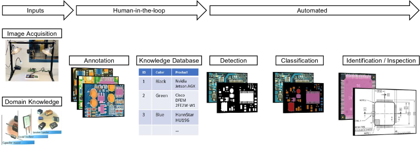
The benefits of golden sample-based \acaoi are significant, but genuine \acpcbas are often not available. When boards are past their supported life span (as is common for long-term government/military applications), highly customized, poorly documented, or of unknown origin, there is often little to no information available about the board, let alone golden images for differential image analysis. Alternative assurance methods must be employed to achieve necessary results. In contrast to golden-based \acaoi, these methods must localize / characterize regions of interest and extrapolate relevant information in place of differential analysis. This is typically performed using a machine learning backbone and significant amounts of labeled data, as shown in Figure 2.
Component identification is responsible for analyzing previously acquired results and making an assurance assessment. During this process, elements of the physical sample are compared to ideal design standards to find likely evidence of manipulation or defects. In this manner, while the precise metrics for a genuine sample are not known beforehand, evidence of tampering will appear as regions which violate \acpdrc, fall outside \acipc standards, do not correspond to a logical netlist/BoM extraction, or exhibit related deviations from expected behavior. In this vein, AutoBoM is a proposed framework which attempts to leverage this information, creating a tentative BoM from optically gleaned information and comparing it to known general component properties (azhagan_new_2019, 29). Lin et al. employ a coupled system of \acocr and image analysis to identify \acpic with clear and blurry text in \acpcb images (lin_using_2019, 36).
As described earlier, datasets play a critical role in the quality of machine learning-based assurance methods. Increasingly complex methods are developed for golden-less \acaoi, but these techniques are heavily stunted without prior growth in the associated datasets. Thus, a discussion of currently available datasets provides reasonable insight into how robust current methods can be expected to perform and how much room for model architecture growth exists.
2.3. Existing Datasets
Several publications introduce datasets useful for \acaoi/\acml methods, each highlighting different aspects of optical \acpcb inspection. While some focus on surface-mount devices, others provide information on connectivity such as traces and vias. The datasets are grouped into two categories below based on whether they are publicly accessible, ordered by the year they were introduced. These are summarized in addition to the proposed \acfpic dataset in Table 1.
Notably, there are far fewer datasets for \acpcb assurance than standard computer vision solutions, such as cell counting, aerial photos, and generic image segmentation (pramerdorfer_dataset_2015, 37). This is a critical issue for a field like hardware assurance, since significant data is one of the few robust mechanisms to combat a dynamically evolving environment (moganti_automatic_1996, 5). As of 2021, the largest publicly available datasets consist of at most 165 \acpcb samples and at most 8,016 unique \acsmd annotations (PCB-DSLR and WACV respectively, see Section 3). As a consequence, this increase in \acml applications for \acpcb assurance without corresponding levels of data does not equate to increased reliability and confidence metrics. These concerns can be addressed either with smaller \acml architectures or larger amounts of ground truth data. While data augmentation can partially address this issue, a large set of unique, representative data is essential for generalizable assurance, especially when tested on deep neural networks (larochelle_exploring_2009, 38).
2.3.1. Publicly Available
CD-PCB (2021) (fridman_changechip_2021, 31). Fridman et al. provide 17 image pairs where each set contains images with and without synthetic defects. This dataset can provide insight into the general, board-level characteristics of defective samples.
Amazon lookout (2021) (ganapathy_defect_2021, 32). Ganapathy and Gupta demonstrate an AWS workflow to identify anomalous versus normal \acppcb based on high-resolution optical images. Without instance-level labels, usability is constrained to high-level defect detection and general characteristic analysis. Nonetheless, they demonstrate reasonable accuracy in discriminating normal and anomalous samples with a given machine learning model.
IC-ChipNet (2020) (reza_icchipnet_2020, 39). Reza and Crandall present a curated bank of over 6,000 \acic images. While they do not provide general text annotations, each \acic is labeled with its manufacturer and several unique logos per manufacturer are represented. This dataset is useful for fine-grained retrieval, recognition, and verification of \acic images.
PCBExperiment (2020) (karanth_pcbexperiment_2020, 40). Not associated with a specific publication or method, this publicly available dataset consists of several hundred defective and non-defective \acpcb samples. Its category depends on whether it passed a manual quality assurance check. Similar to Amazon Lookout above, no other annotations or instance-level attributes are defined in this dataset. However, as with CD-PCB it can be useful for generalizing traits of poor-quality boards or defective samples.
FICS-PCB (2020) (lu_ficspcb_2020, 17). Over 400 images were collected of 31 \acpcb samples in this work. A combined total of 30,000 \acsmd bounding boxes are present across these duplicate images, with several pieces of metadata associated with each component. More information is visible in Table 1. The comprehensive data collected is useful for a variety of purposes, including resolution requirement analysis, component localization & classification, and character recognition.
WACV (2019) (kuo_dataefficient_2019, 41). Kuo et al. provide one of the first public datasets with board text annotations. With over 6,000 component annotations and 10,000 text annotations across 41 \acpcb images, they allow for a dynamic array of new machine learning tasks in addition to component detection and localization.
HRIPCB (2019) (huang_pcb_2019, 22). Huang and Wei present this dataset containing 10 \acpcb images with multiple synthetic defects. In each case, bounding box annotations around each defect location are provided. Compared to (karanth_pcbexperiment_2020, 40, 31), these annotations provide more precise and detailed information about defect compositions.
PCB-DSLR (2015) (pramerdorfer_dataset_2015, 37). One of the first public \acpcb datasets, Pramerdorfer and Kampel paved the way for machine learning applications with this contribution. The dataset contains 165 unique \acppcb and over 2,000 labeled \acic instances with text data for a small subset. More images are captured in different orientations, increasing the size of data when label repetitions are considered.
2.3.2. Out-of-Scope
Several additional works highlight datasets that either are not publicly available or do not directly handle \acpcb/\acsmd images. (gang_coresets_2020, 42) presents a sizable dataset of \acpcb images at a production plant and labels “coresets” of \acocr characters, which are building blocks for more flexible text-based model training. No public link is given, but the authors note in (gang_character_2021, 43) that data is available upon request. DEEP-PCB (2019) provides a dataset of annotated substrate defects. Images consist of post-thresholding via/trace masks rather than the raw optical data (tang_online_2019, 44). A dataset of google images seeded by PCB-DSLR is presented by Chen et al. (chen_addressing_2017, 45), but this curated and annotated list of images is not publicly available. (li_multisensor_2021, 46) collects multimodal data including \acir and visible images of \acpcb defects, but is not publicly accessible. (shieh_applying_2021, 47) demonstrates the performance of a new YOLO (v5) architecture specifically designed to locate tiny defects in high-resolution quality-control \acpcb images. PCB-METAL presents a large dataset of high-resolution \acpcb images similar to FICS-PCB, but there is no public link to the data and fewer representative component types are labeled (mahalingam_pcbmetal_2019, 48).
3. FPIC Dataset
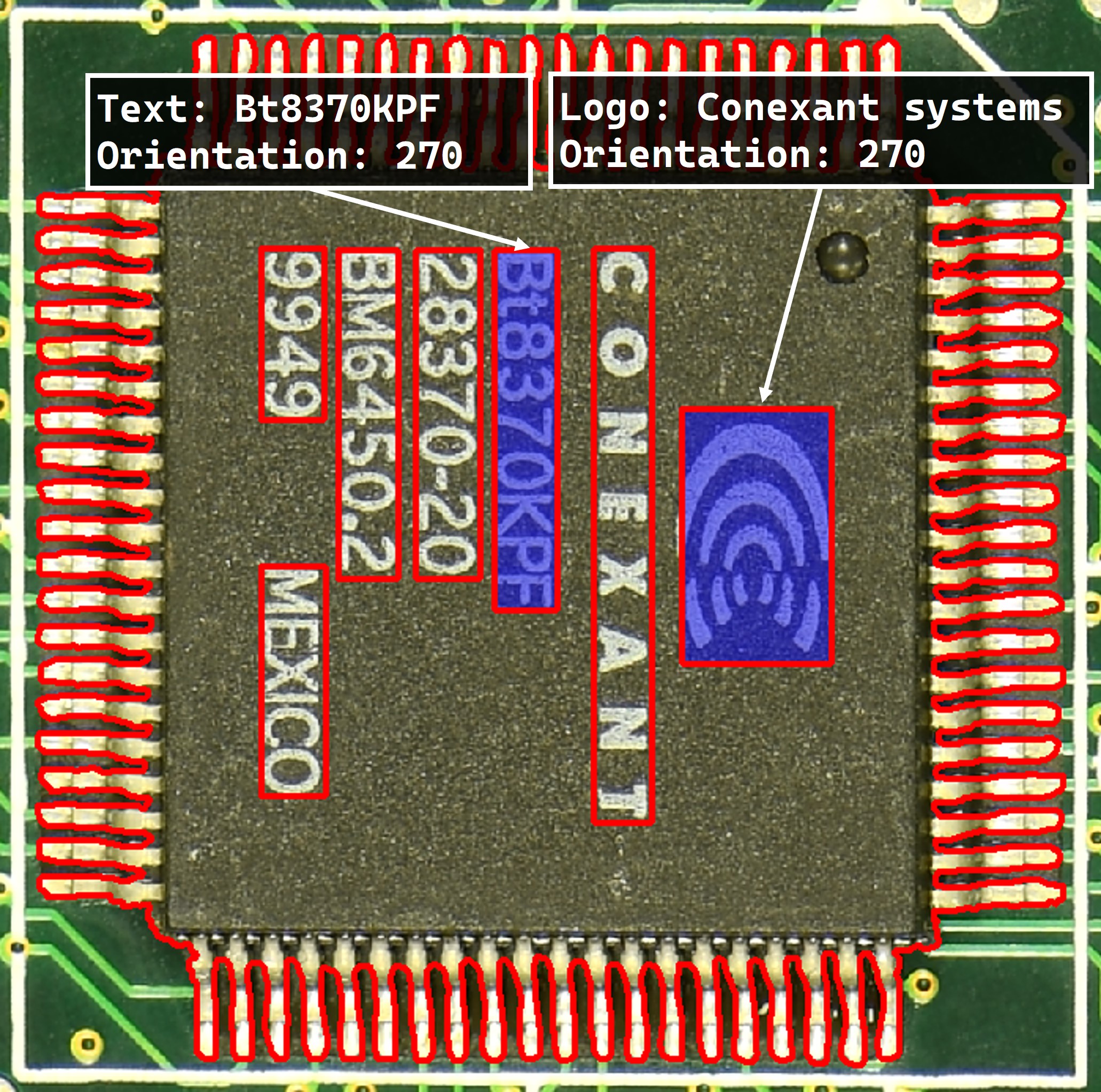
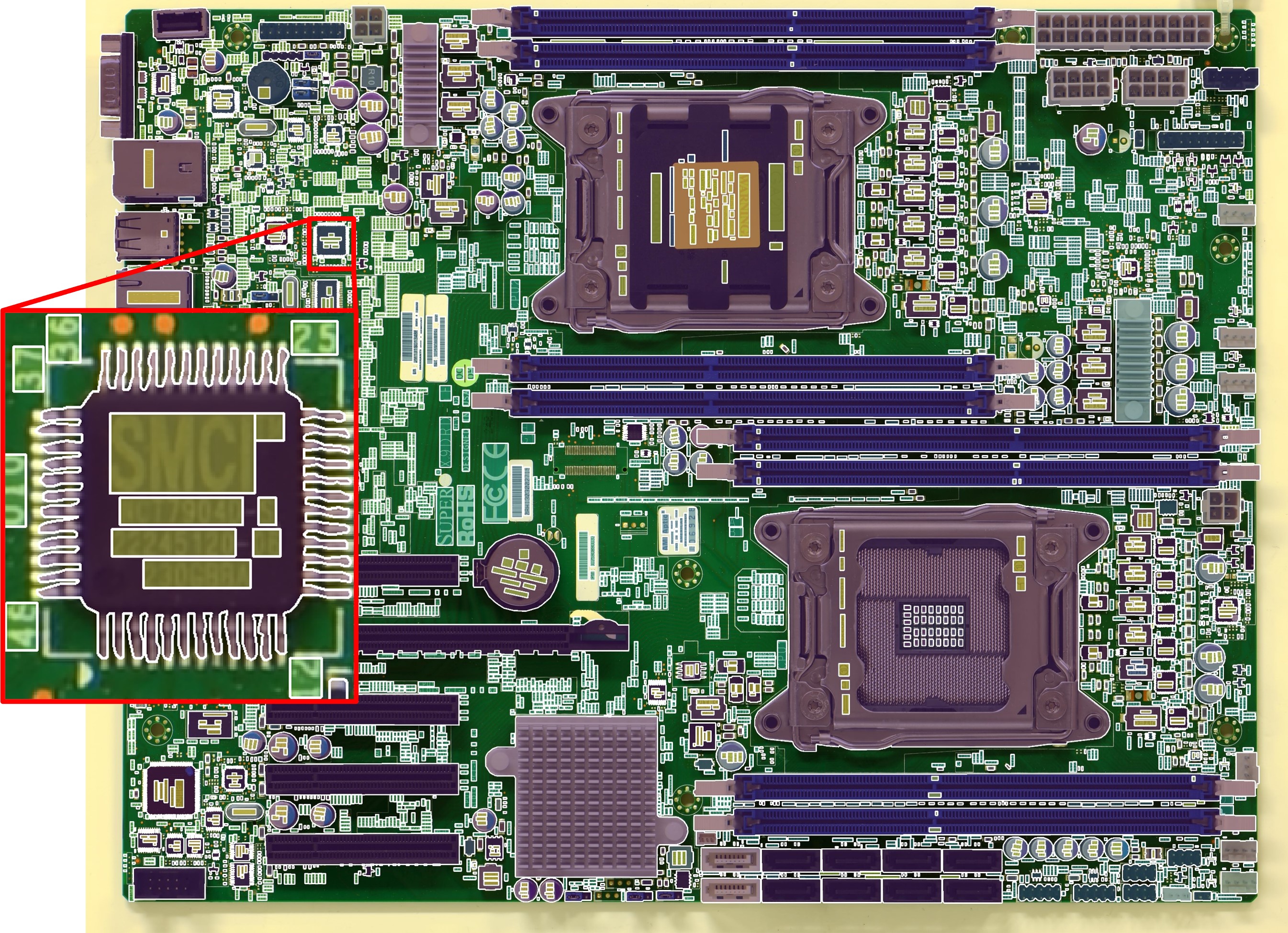
As noted previously, the \acfpic dataset was developed to address data availability bottlenecks in \acml-based \acaoi methods. The dataset consists of 261 images of 93 separate \acppcb. Note that more images exist than physical \acpcb samples since both front and back images can be acquired, and some \acppcb are photographed in multiple settings. Both text and mounted components are annotated where applicable in most images, resulting in over 71,000 annotated instances. \acpcb samples were purchased online or disassembled from a variety of different devices, e.g. computer hard drive controllers, servers, and audio amplifiers. An example image with annotations is shown in Figure 3. \acfpic’s creation and the rationale for included metadata is explained in the following subsections. Critically, this dataset will continue to grow larger over time as more samples are cataloged and annotated.
fpic’s dataset statistics in comparison to other works is shown in Table 1, though fairly comparing FPIC to prior datasets is deceptively challenging. Comparing quantity of ground truth annotations between datasets requires that a distinction be made between unique and total instances: one \acpcb might be photographed and annotated four times, but only one set of those annotations provide new information because the remaining three images are simply geometric transforms of the first. Machine learning algorithms must be careful to distinguish between these when using training sets, otherwise they risk treating augmentations as unseen samples. In an effort to compare datasets as fairly as possible, Table 1 lists both the total and unique annotation quantities for datasets with duplicate annotations.
![[Uncaptioned image]](/html/2202.08414/assets/x2.png)
3.1. Imaging
Images were taken in controlled conditions with a Nikon D850 DSLR camera. A two-second delay mitigated camera shake during acquisition, and a two-second exposure reduced image noise. Each time the camera position or zoom changed, a calibration photo of an X-Rite Passport or Nano Color Checker was collected to normalize colors across changing environmental conditions (e.g., photographs taken with different amounts of natural light). A portion of the dataset consists of the same \acpcb samples imaged under several illumination and camera sensor parameters to study the effects of normalization (paradis_color_2020, 49).
Each image in the database consists of a single photograph rather than a stitched sequence of tiles. While image stitching is common to increase resolution, it introduces defects such as distortion / warping, imperfect alignment, and noise at stitching boundaries. A thorough investigation of these defects can be found in (lu_ficspcb_2020, 17). \acfpic optimizes for minimal processing and noise reduction at the expense of lower resolution for very large samples.
3.2. Contour Annotation
Collected images were processed using S3A (https://gitlab.com/s3a/s3a) and SuperAnnotate (www.superannotate.com). The SuperAnnotate service was responsible for creating high-fidelity semantic outlines around components in a subset of \acpcb images as well as creating bounding boxes around device and board text. A significant number of images were annotated in-house using S3A, where assistance algorithms such as GrabCut and K-Means segmentation simplified this process. All contours (bounding box or otherwise) are represented as lists of polygons indicating either holes or foreground areas.
3.3. Metadata Annotation
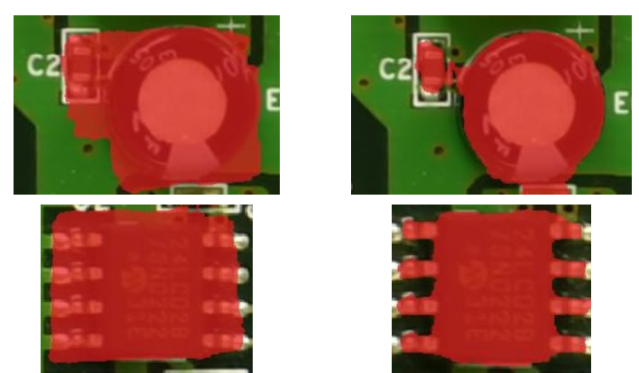
Once gathered, component and text boundaries were loaded into S3A where the remaining metadata (Text, Logo, Designator, etc.) was added locally. Since complex \acsmd contours were extraordinarily time-consuming to obtain, the only additional metadata associated with these instances was the “Designator”: silkscreen board text containing the component identifier such as ‘C’, ‘L’, ‘R’, etc. If no designator was present, instead of attempting to infer the proper label, we opted not to assign a label to avoid adding potentially incorrect component labels. Figure 4 illustrates one scenario where similar-looking components could easily be misidentified if annotators tried to guess component identity instead of relying only on designators.

3.4. Validation
Each file underwent two rounds of manual validation and a logical check to minimize the number of human errors present in the final version. The logical check programmatically searched for edge cases such as replicated components in the same file, duplicate metadata, strongly overlapping regions, and other factors usually indicative of errors during annotation.
Unlike \acsmd components, \acocr instances have a host of associated metadata, including some fields that are present for the first time in \acpcb dataset literature. These are summarized in Table 2.
![[Uncaptioned image]](/html/2202.08414/assets/x3.png)
3.5. Database insertion
The \acfpic dataset is stored on TrustHub; Table 3 summarizes the database’s directory structure. Beyond metadata for labeled instances, each image is associated with scale information to enable measurement of physical dimensions based on pixel counts, a color checker, and a camera model. The first 150 images in \acfpic use the same \acpcb samples at different scales to evaluate the effects of resolution on component detectability as done in (lu_ficspcb_2020, 17).
Beyond color and scale calibration parameters, over three-fourths of the \acpcb samples also possess a brief functional description, i.e. “Honeywell 14500144-001 Module PLC PCB Board”. This information enables searching for documents like data sheets or \accad files if desired.
![[Uncaptioned image]](/html/2202.08414/assets/x4.png)
4. Methodological insights
After years of data collection, we learned important lessons as a result of sample diversity, variance between annotators, and acquisition volume. The metadata collected by \acfpic (namely, semantic contours and silkscreen-to-component association) that was not included in prior work also yielded useful insights. These are explained in the following paragraphs, separated into imaging and logistical categories. Each subsection provides a handful of recommendations for improving future data collection.
4.1. Imaging challenges
Imaging challenges include imaging irregularities and particularities that can be resolved by altering the image acquisition setup. The examples below illustrate cases where artifacts of the imaging process alter ground truth markings depending on the details present in annotation instructions and annotator skill.
![[Uncaptioned image]](/html/2202.08414/assets/x5.png)
Occluded components and markings. Some, but not all, occluded components and markings can be revealed by slightly adjusting the angle from the sample to the camera. Many markings that would be valuable for assurance, e.g., polarity markers, component symbols, or designators, are located directly beneath mounted components to assist in manual assembly or rework. Unfortunately, it is usually impossible to completely image these markings even when multiple camera angles are considered.The top row of Table 4 illustrates this challenge. When considering occluded components, the output segmentation often varies across annotators since some may consider only the visible portion of a device while others will extrapolate its position.
Reflective components and conformal coating. Reflections also negatively impact the ease of annotation and feature detection. Conformal coating is typically applied to \acppcba requiring environmental hardening, resulting in a sheen across short components. This effect is stronger with direct lighting. As a result, it can be difficult to determine the true color or shape of the covered device, leading to misclassification or poor boundaries. Additionally, direct lighting across tall components can reflect bright areas of the board resulting in artifacts like the right side of row 2. Note that annotation instructions do not often outline a procedure for these cases, so artifacts may appear as ground truth annotations when working with low-cost or minimal QA annotation pipelines. However, applying a polarized filter to the camera can greatly reduce these specular side effects. If more control can be gained over the imaging environment, these effects can also be mitigated through precise lighting or stereophotographic acquisition.
Ambiguity between mounted/unmounted pads. Components that share colors with the PCB substrate complicate the distinction between populated vs. unpopulated solder pads. As a result, annotators can mistake the two and increase the difficulty in training a neural network to locate \acpsmd. Row 3 illustrates the difference between a green SMD and silkscreen between empty pads. Note that the depicted example is straightforward to resolve due to the high-resolution image, but a low-resolution counterpart greatly increases the difficulty. Two simple methods exist for increasing resolution: adjusting the zoom or exposure time of the image. While increasing the zoom is often preferable, it can lead to more artifacts if image stitching is required as a result. Alternatively, increasing exposure time cuts down on some forms of sensor noise but cannot resolve all forms of resolution-based complexity.
Masked PCB areas. While the first category addressed individually occluded components, another frequent scenario involves large swaths of a PCB covered by various objects like heat sinks, stickers, daughterboards, etc. Depending on the threat model, this eases a malicious actor’s difficulty inserting untrusted components since they can be trivially covered as seen in row 4. Thus, robust inspection mechanisms must determine a way to identify areas of the board likely to contain components masked by a secondary object. A minor amount of sample preparation can avoid several of these concerns. By removing stickers and disconnecting daughter boards before imaging, large amounts of previously obscured circuitry will become visible. When removal is not possible (e.g. heat sinks and daughter boards which must remain attached), subsurface imaging such as X-Ray can be incorporated.
Widely varying component profiles. When components have long leads (i.e. transistors, diodes, crystal oscillators, etc.), they can be contorted into a variety of shapes as viewed from the top down. In these cases, similar to occluded component scenarios, width/length annotations from the top-down object view do not correspond to width/length values from a BoM reference. Annotating additional metadata, such as the location of leads in the image, can assist in determining whether component height, width, or length should be matched to the visible dimensions in the optical image.
4.2. Logistical insights
In contrast to imaging challenges, the following discussion about methodological logistics does not depend on image quality or other environmental factors. Rather, these are fundamental characteristics of an annotation and assurance workflow that attempts to use flowchart rules to encode human design insights. Each heading illustrates the difficulties of correlating silkscreen information with PCB design characteristics.
![[Uncaptioned image]](/html/2202.08414/assets/x6.png)
Greatly separated designators and SMDs. Ideally, designators are close to their associated components and unlikely to be confused with neighboring designators. However, this is not the case in densely populated PCB regions where component real estate imposes stringent requirements. In these scenarios, several designators are grouped together, placed in an open area on the board, and ‘linked’ in some manner to a corresponding group of components as shown in Table 5 row 1. The way in which links are formed depends entirely on the PCB designer; cluster labels, arrows, and orientation matching are common approaches, but there are others. These common approaches enable development of heuristics that may be able to associate designators with components in the common case, but as long as designator placement remains a stylistic decision it will be difficult to confidently automate associations.
Reference designator agglomeration. When several designators are clustered as previously described and all refer to a sequential group of similar component types (i.e. a row of resistors/capacitors), one approach is to create a single label for all components. Various manifestations of this principle are illustrated in row 2. Since there are no design standards for how this grouping must take place, where silkscreen must be located relative to components, or how the association is made between a component and its text, understanding and annotating this association is difficult. Additionally, these cases demonstrate how silkscreen-to-component associations are not a one-to-one mapping: a single silkscreen can refer to multiple components and multiple silkscreens can belong to the same component (this is fairly common in IC or header pin annotations).
Run-on designator clusters. The same space restrictions explained in the first paragraph can cause groups of designators to run into each other and appear as one long text string. Humans can usually intuit the designer’s intent, but these run-on designators can complicate automatic component designator extraction using off-the-shelf OCR methods. In the example shown in row 3, not only are designators prefixed with an integer character (“C4V”), but are close enough to nearby designators that whitespace cannot be used as token separator.
Mismatched silkscreen vs. component. From an assurance perspective, this is one of the most challenging scenarios to address. In prior works, independent silkscreen and component annotations could both be considered valid as shown in the first two figures of row 4. However, the component in question clearly does not match its reference designator. “L” is most commonly reserved for inductors, while “R” is almost exclusively used for resistors. From their appearance, the associated \acpsmd are clearly a resistor and capacitor, respectively. As such, while the components are properly mounted and the text is legible, there is an error in their association. Similarly, the third figure in this row illustrates a duplicate silkscreen marking. Both are correct for their associated component and legible, but the duplicate reference is highly abnormal and likely indicates a silkscreen mistake. In cases like these, determining whether the error is with the design, silkscreen print, or mounted component creates challenges for assurance.
Non-text silkscreen. Beyond alphanumeric characters, a host of various additional information is printed on the PCB substrate. As described in Section 4.1, silkscreen can also refer to mounting information. However, a common theme is that silkscreen is primarily intended for human evaluation and has no uniform representation. Hence, without a catalog of common templates, it can be complex to algorithmically derive alignment information as presented in row 5 of Table 5. In the first instance, the polarity of a capacitor is presented with double arrows that should match the on-device markings present. Secondly, the obscured Zener diode symbol indicates polarity with a vertical line that should match the black bar present on the mounted component. Finally, the most complex case involves overlapping silkscreens where a left-facing triangle indicates the position of an IC’s first pin. In each case, a vastly different visual cue is used to indicate alignment. These complexities drastically complicate how features such as polarity should be represented in an annotation database.
Designators for unmounted components. The final highlighted case for methodological insights involves designator associations with unpopulated solder pads. Technically, the designator does not refer to the pads, but the missing component meant to reside between them. At the same time, the pads are a reasonable approximation of the same spatial location associated with the text. Hence, there is justifiable reasoning for both including and excluding a correlation indicator for the silkscreen in question. Moreover, if a component association is created, it is unclear whether it belongs to one or multiple pads. Each of these considerations complicates the process of generating ground truth labels in this circumstance. during FPIC annotation, the pad closest to the designator is given the association.
5. Newly enabled research
fpic is larger and contains more diverse \acpcb examples than prior \acpcb image datasets, making it a better input to \acml training and a better benchmark for validating optical assurance techniques. Additionally, its annotations include novel information that enables new optical assurance research. The following paragraphs elucidate the connections between specific \acpcb assurance challenges and data that is collected for the first time in \acfpic.
5.1. Dataset size and diversity
The left-hand side of Figure 2 emphasizes that optical assurance must be calibrated for the \acpcb under inspection and the threat to be detected. \acppcb exhibit tremendous diversity across many characteristics that could impact optical assurance performance. For example, densely-packed boards, smaller components, or more sophisticated counterfeiting might all require higher imaging resolution to enable successful assurance. If a dataset is systematically biased with regard to imaging-relevant characteristics (e.g., a dataset containing boards of a similar manufacturing year, similar application domain, similar types of components, etc.), this may bias \acml networks trained on the data and limit the generality of performance claims that can be made for techniques that are validated against the dataset. Increasing the number and variety of represented \acppcb and annotated components is the best hedge against these pitfalls.
As summarized in Table 1, \acfpic is significantly larger and more generalized than in prior work. It possesses more labeled \acpcb samples and drastically more unique component annotations than the leading prior work. Among several other significant benefits, we highlight that a larger dataset allows tighter confidence margins on statistical analysis, enables \acfpic to display more optical inspection corner cases, and provides more data for training large \acai networks. Notably, \acfpic will continue to grow over time as more \acppcb and annotations are added. As the technology landscape evolves, it is necessary to re-evaluate whether the dataset remains representative of boards to-be-assured.
While dataset size is important, it cannot stand alone as a metric of dataset quality; diversity of examples in the dataset is equally important. \acfpic was purposefully built to include \acppcb from many application domains, built by different \acpoem, manufactured in a range of years, and obtained from a variety of distributors in a variety of conditions. This intentional variation ensures that \acfpic is representative of the broader population of printed circuit boards. This will help \acai models trained on \acfpic to perform well on systems they have never seen and reduces bias when \acfpic is used to validate optical assurance techniques. Manufacturing date, \acpcb function, manufacturer, distributor, etc. are qualitative and imprecise proxies for dataset diversity. Currently, there are no precise, measurable characteristics for describing a population of \acppcb from an imaging perspective, but additional research will be able to standardize such metrics. Here, too, \acfpic can provide insight. Its size and diversity enable studies to determine the most imaging-relevant \acpcb characteristics.
5.2. Improved SMD contour analysis from semantic segmentation
Overwhelming amounts of literature demonstrate the usefulness of semantically segmented ground truth for enhanced machine learning capabilities (garcia-garcia_review_2017, 50, 51, 52, 53, 54). While segmentation is possible with automated methods, the outputs are not consistently defect-free without significant hyperparameter tuning. In other words, high-quality automated segmentation still requires a large amount of human oversight in the segmentation architecture and parametrization. However, neural networks trained on human-verified segmentation masks overcome these difficulties with enough diverse ground truth data. The paragraphs below detail several ways machine learning tasks trained using segmentation ground truth rather than bounding boxes yield significantly improved outputs.
Component localization. While bounding box data can reasonably train a network to find components on a PCB, semantically trained networks can take this one step further. Figure 5 shows that predictions overlap for nearby components in a bounding-box-trained LinkNet architecture versus its semantic counterpart. All aspects of training were the same in both cases except the masks.
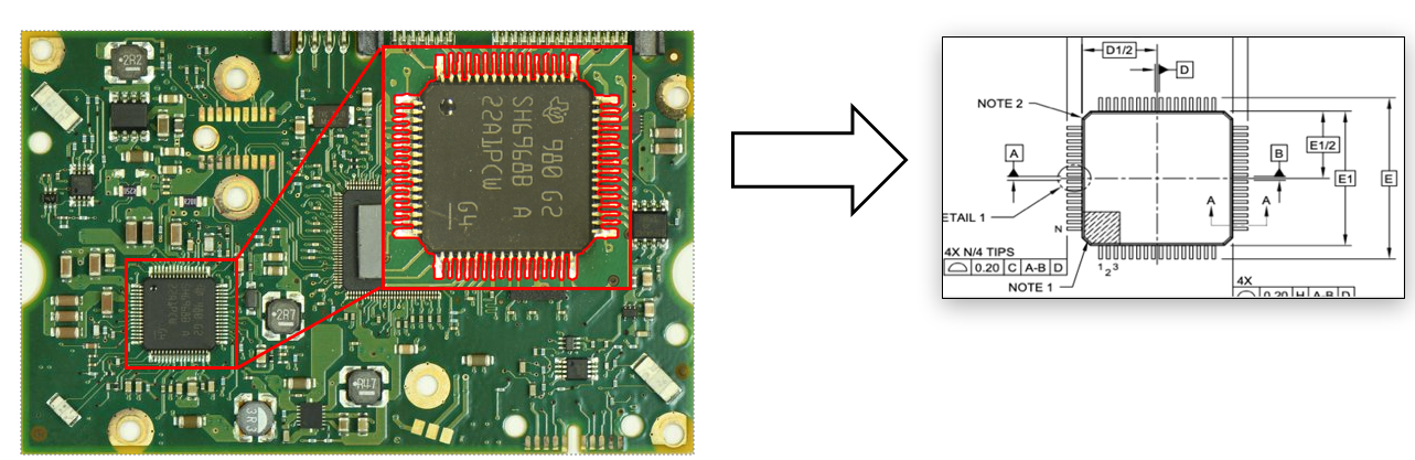
BoM property extraction. Multiple component footprint properties such as pin count, pitch, width, and spacing can only be determined with accurate outlines. FPIC provides enough of these samples to allow property extraction on unseen data as well by training semantic segmentation networks on the ground truth information. This drastically improves the ability of assurance algorithms to cross-reference known component properties against IPC standards and datasheet specifications. Figure 5 also shows how a semantically trained ML model accurately represents IC contours with sufficient training data. Figure 6 illustrates how these contours can be directly translated into BoM properties.
Assembly analysis. Beyond the component itself, how a device is mounted on the PCB can also be analyzed more fully with semantic contours. The difference between an oblong and right-angled device can yield insights as to whether the mount is within tolerance or is defective. Similarly, heavily skewed pins from tall through-hold components can be readily identified with precise boundaries and would otherwise not stand out with traditional bounding box annotations.
5.3. Schematic analysis from component locator association
Often, silkscreen designator information is critical to identifying the function or type of component present in an optical image. As such, identifying which components are associated with what board text can result in a significant boost in identification capabilities.
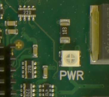
DRC Analysis. Text such as “PWR” or “GND” can be associated with the substrate itself rather than / along with a component. In these cases, aspects of the board layout can be analyzed in light of this silkscreen information to ensure both are in agreement. Figure 7 demonstrates how the larger width requirement for power traces can be evaluated in light of the associated silkscreen identifier.
Designator Verification. Datasheets and BoMs often make heavy use of pin numbers and reference designators (i.e. “R101”, “L2”, etc.). Since the association between components and their text can be highly nontrivial (see Section 4.2), ground truth markers for this information are highly valuable for automated inspection efforts. When the designator is correct, and the SMD looks good, only the component locator can indicate whether there is a mismatch.
Assembly verification. As noted in Table 5, several types of silkscreen identifiers assist in determining device orientation or polarization. Hence, additional research objectives can bring an orthogonal dimension of assurance inspection to the traditional optical image analysis workflow.
Chatterjee et al. describe an augmented reality system that quickly correlates design schematics with hardware to simplify the process of quality assurance and HW/SW context switching (chatterjee_augmented_2021, 55). Data from FPIC would allow such a system to rely less on software schematics for similar offerings when few design files are present.
5.4. Data balance through parametrized acquisition
Beyond the annotated metadata, much information about the PCB samples themselves is also collected. By combining information about real-world image scale, PCB manufacturer, and board description, SMD information can be correlated against additional factors other than their optical appearance. For instance, novel research directions might include evaluating whether certain manufacturers prefer specific brands or ratings of passive components. Or, whether defects and annotation errors occur more frequently for some sample categories. Significantly, the descriptive information associated with each board can be tied to relevant datasheets and CAD information for multiple samples, allowing schematic-level verification of collected information.
6. Conclusion and Future Work
In conclusion, we have reviewed state-of-the-art techniques for \acaoi and observed the strong, rapid trend toward \acml solutions. These require significant amounts of labeled ground truth data, which is lacking in the publicly available \acpcb data space. The \acfpic dataset (https://www.trust-hub.org/#/data/pcb-images) is proposed to address this bottleneck in available large-volume, diverse annotations. Additionally, this work covers the potential increase in hardware security capabilities and observed methodological distinctions highlighted during data collection.
Via, Trace, Pin Annotation. Future releases of the \acfpic dataset will include annotations of vias, traces, and pins across a board’s surface. This will yield significant insights into cross-component connectivity, the relationship between components and substrates, signal frequency analysis through trace layout inspection, and much more.
Synthesized \acpcb samples. Beyond annotating purchased physical samples, future iterations can include fully synthesized \accad renderings and compare digital versus real-world annotation results. In this manner, the \acfpic dataset could be drastically increased by providing augmented virtual counterparts. Moreover, a subset of these samples could be fabricated to determine more accurate relationships between design schematics and the acquired optical data. In this vein, Calzada et al. demonstrated several challenges inherent in optical \acpcb inspection by designing custom samples with various intentional defects and Trojans, ranging from easy to difficult detection criteria (paul_gomac, 56).
Track related \accad schematics and datasheets. Along with physical samples, the item description is associated with datasheets or development files in several cases. Collecting this information in addition to each board will greatly increase the ability to provide \achw assurance through cross-referencing against known circuit properties. Additionally, these files would increase the accuracy of ground truth annotations since they provide references for the type and characteristics of each mounted component.
Multimodal data fusion. The \acfpic dataset is a valuable resource for \acaoi research, but does little to address volumetric issues, material properties, etc. Toward this end, increased data acquisition and rigorous labeling in other modalities such as X-ray, \acthz, and similarly neglected modalities would greatly assist additional assurance objectives. Active efforts in this direction are underway by the \acfics group (mehta_fics_2022, 57), but as explained below it will be essential for additional collaborators to join this process.
Continuous collection and collaboration. A major theme throughout this work is the importance of publicly available data from a diverse array of sources and annotators. Continuous collaboration with the hardware assurance and computer vision communities at large is essential for growth in \acaoi capabilities. More than just data alone, these enhancements would include code libraries, frameworks, standards, and evaluation mechanisms/metrics for improving the baseline for quality ground truth annotations. The \acfpic dataset will continue to grow in the near future, and this increased coordination and collaboration will ensure the quality and fidelity of the dataset only improves in that course.
References
- (1) J. Robertson and M. Riley “The Big Hack: How China Used a Tiny Chip to Infiltrate U.S. Companies”, 2018 URL: https://www.bloomberg.com/news/features/2018-10-04/the-big-hack-how-china-used-a-tiny-chip-to-infiltrate-america-s-top-companies
- (2) Jacob Appelbaum et al. “NSA’s Secret Toolbox: Unit Offers Spy Gadgets for Every Need” In Der Spiegel, 2013 URL: https://www.spiegel.de/international/world/nsa-secret-toolbox-ant-unit-offers-spy-gadgets-for-every-need-a-941006.html
- (3) Jacob Harrison, Navid Asadizanjani and Mark Tehranipoor “On malicious implants in PCBs throughout the supply chain” In Integration 79, 2021, pp. 12–22 DOI: https://doi.org/10.1016/j.vlsi.2021.03.002
- (4) “Investigation into counterfeit electronic parts in the department of defense supply chain”, 2012
- (5) Madhav Moganti, Fikret Ercal, Cihan H. Dagli and Shou Tsunekawa “Automatic PCB Inspection Algorithms: A Survey” In Computer Vision and Image Understanding 63.2, 1996, pp. 287–313 DOI: 10.1006/cviu.1996.0020
- (6) Johannes Richter, Detlef Streitferdt and Elena Rozova “On the Development of Intelligent Optical Inspections” In 2017 IEEE 7th Annual Computing and Communication Workshop and Conference (CCWC), 2017, pp. 1–6 DOI: 10.1109/CCWC.2017.7868455
- (7) Ujjwal Guin et al. “Counterfeit Integrated Circuits: A Rising Threat in the Global Semiconductor Supply Chain” In Proc. IEEE 102.8 IEEE, 2014, pp. 1207–1228 DOI: 10.1109/JPROC.2014.2332291
- (8) Brian Grow et al. “Dangerous fakes” In Bloomberg Businessweek, 2008
- (9) Matthew McGuire, Umit Ogras and Sule Ozev “PCB Hardware Trojans: Attack Modes and Detection Strategies” In 2019 IEEE 37th VLSI Test Symposium (VTS), 2019, pp. 1–6 DOI: 10.1109/VTS.2019.8758643
- (10) Andrew Huang “Keeping secrets in hardware: the Microsoft XBox case study” AI Memo 2002-08 MIT AI Lab, 2002
- (11) Shahed E. Quadir et al. “A Survey on Chip to System Reverse Engineering” In J. Emerg. Technol. Comput. Syst. 13.1, 2016 DOI: 10.1145/2755563
- (12) L.S. Watkins “Inspection of Integrated Circuit Photomasks with Intensity Spatial Filters” In Proceedings of the IEEE 57.9, 1969, pp. 1634–1639 DOI: 10.1109/PROC.1969.7348
- (13) Wei-Chien Wang, Shang-Liang Chen, L. Chen and Wan-Jung Chang “A Machine Vision Based Automatic Optical Inspection System for Measuring Drilling Quality of Printed Circuit Boards” In IEEE Access, 2017 DOI: 10.1109/ACCESS.2016.2631658
- (14) A.. Hani, A. Malik, Raja Kamil and C. Thong “A Review of SMD-PCB Defects and Detection Algorithms” In Other Conferences, 2012 DOI: 10.1117/12.920531
- (15) Peng Wei et al. “CNN-based Reference Comparison Method for Classifying Bare PCB Defects”, 2018 DOI: 10.1049/JOE.2018.8271
- (16) Linlin Zhang et al. “Convolutional Neural Network-Based Multi-Label Classification of PCB Defects”, 2018 DOI: 10.1049/JOE.2018.8279
- (17) Hangwei Lu et al. “FICS-PCB: A Multi-Modal Image Dataset for Automated Printed Circuit Board Visual Inspection”, 2020 URL: http://eprint.iacr.org/2020/366
- (18) SeungGeun Youn, YounAe Lee and TaeHyung Park “Automatic Classification of SMD Packages Using Neural Network” In 2014 IEEE/SICE International Symposium on System Integration, 2014, pp. 790–795 DOI: 10.1109/SII.2014.7028139
- (19) Venkat Anil Adibhatla et al. “Detecting Defects in PCB Using Deep Learning via Convolution Neural Networks” In 2018 13th International Microsystems, Packaging, Assembly and Circuits Technology Conference (IMPACT), 2018 DOI: 10.1109/IMPACT.2018.8625828
- (20) Dae-ui Lim, Young-Gyu Kim and Tae-Hyoung Park “SMD Classification for Automated Optical Inspection Machine Using Convolution Neural Network” In 2019 Third IEEE International Conference on Robotic Computing (IRC), 2019, pp. 395–398 DOI: 10.1109/IRC.2019.00072
- (21) Young-Gyu Kim, Dae-Ui Lim, Jong-Hyun Ryu and Tae-Hyoung Park “SMD Defect Classification by Convolution Neural Network and PCB Image Transform” In 2018 IEEE 3rd International Conference on Computing, Communication and Security (ICCCS), 2018, pp. 180–183 DOI: 10.1109/CCCS.2018.8586818
- (22) W. Huang and P. Wei “A PCB Dataset for Defects Detection and Classification” arxiv.org, 2019 arXiv: https://arxiv.org/abs/1901.08204
- (23) Ujjwal Guin, Daniel DiMase and Mohammad Tehranipoor “A Comprehensive Framework for Counterfeit Defect Coverage Analysis and Detection Assessment” In Journal of Electronic Testing 30.1, 2014, pp. 25–40 URL: https://doi.org/10.1007/s10836-013-5428-2
- (24) Martin Goetz and Ramesh Varma “Counterfeit Electronic Components Identification: A Case Study”, 2017
- (25) Huihui. Wu, Guanglin. Feng, Huiwen. Li and Xianrong. Zeng “Automated Visual Inspection of Surface Mounted Chip Components” In 2010 IEEE International Conference on Mechatronics and Automation, 2010, pp. 1789–1794 DOI: 10.1109/ICMA.2010.5588029
- (26) Mark Tehranipoor, Ujjwal Guin and Swarup Bhunia “Invasion of the Hardware Snatchers: Cloned Electronics Pollute the Market” In IEEE Spectrum, 2017
- (27) Pangolin Laser Systems “Recognize Counterfeit FB3-QS” URL: https://pangolin.com/pages/recognise-counterfeit-fb3-qs
- (28) Lily Hay Newman “The Anatomy of a Cisco Counterfeit Shows Its Dangerous Potential” In WIRED, 2020 URL: https://www.wired.com/story/counterfeit-cisco-switch-teardown/
- (29) Mukhil Azhagan et al. “A New Framework for Automatic Bill of Material Generation and Visual Inspection” In International Symposium on Test and Failure Analysis (ISTFA), 2019
- (30) Navid Asadizanjani, Mark Tehranipoor and Domenic Forte “PCB Reverse Engineering Using Nondestructive X-ray Tomography and Advanced Image Processing” In IEEE Transactions on Components, Packaging and Manufacturing Technology 7.2, 2017, pp. 292–299 DOI: 10.1109/TCPMT.2016.2642824
- (31) Yehonatan Fridman, Matan Rusanovsky and Gal Oren “ChangeChip: A Reference-Based Unsupervised Change Detection for PCB Defect Detection” arXiv: 2109.05746 In arXiv:2109.05746 [cs], 2021 URL: http://arxiv.org/abs/2109.05746
- (32) Prashanth Ganapathy and Amit Gupta “Defect Detection and Classification in Manufacturing Using Amazon Lookout for Vision and Amazon Rekognition Custom Labels”, 2021 Amazon Web Services URL: https://aws.amazon.com/blogs/machine-learning/defect-detection-and-classification-in-manufacturing-using-amazon-lookout-for-vision-and-amazon-rekognition-custom-labels/
- (33) Thomas Jose Mazon De Oliveira, Marco Aurelio Wehrmeister and Bogdan Tomoyuki Nassu “Detecting Modifications in Printed Circuit Boards from Fuel Pump Controllers” In 2017 30th SIBGRAPI Conference on Graphics, Patterns and Images (SIBGRAPI), 2017, pp. 87–94 DOI: 10.1109/SIBGRAPI.2017.18
- (34) Huibin Zhao, Jun Cheng and Jianxun Jin “NI Vision Based Automatic Optical Inspection (AOI) for Surface Mount Devices: Devices and Method” In 2009 International Conference on Applied Superconductivity and Electromagnetic Devices, 2009, pp. 356–360 DOI: 10.1109/ASEMD.2009.5306622
- (35) Chien-Chih Wang, Bernard C. Jiang, Jing-You Lin and Chien-Cheng Chu “Machine Vision-Based Defect Detection in IC Images Using the Partial Information Correlation Coefficient” In IEEE Transactions on Semiconductor Manufacturing 26.3, 2013, pp. 378–384 DOI: 10.1109/TSM.2013.2261566
- (36) C.. Lin, S.. Wang and C.. Lin “Using Convolutional Neural Networks for Character Verification on Integrated Circuit Components of Printed Circuit Boards” In Applied Intelligence Springer, 2019 URL: https://link.springer.com/article/10.1007/s10489-019-01486-5
- (37) C. Pramerdorfer and M. Kampel “A Dataset for Computer-Vision-Based PCB Analysis” In 2015 14th IAPR International Conference on Machine Vision Applications (MVA), 2015 DOI: 10.1109/MVA.2015.7153209
- (38) Hugo Larochelle, Yoshua Bengio, Jerome Louradour and Pascal Lamblin “Exploring Strategies for Training Deep Neural Networks” In Journal of machine learning research 10.1, 2009, pp. 40
- (39) Md Alimoor Reza and David J. Crandall “IC-ChipNet: Deep Embedding Learning for Fine-Grained Retrieval, Recognition, and Verification of Microelectronic Images” In 2020 IEEE Applied Imagery Pattern Recognition Workshop (AIPR), 2020 DOI: 10.1109/AIPR50011.2020.9425131
- (40) Namratha Karanth “PCBexperiment” In Kaggle, 2020 URL: https://kaggle.com/namrathakaranth/pcbexperiment
- (41) Chia-Wen Kuo, Jacob Ashmore, David Huggins and Zsolt Kira “Data-Efficient Graph Embedding Learning for PCB Component Detection” In 2019 IEEE Winter Conference on Applications of Computer Vision (WACV), 2019 IEEE
- (42) Sumyung Gang, Ndayishimiye Fabrice and JoonJae Lee “Coresets for PCB Character Recognition Based on Deep Learning” In 2020 International Conference on Artificial Intelligence in Information and Communication (ICAIIC), 2020, pp. 637–642 DOI: 10.1109/ICAIIC48513.2020.9065271
- (43) S. Gang, Ndayishimiye Fabrice, Daewon Chung and JoonJae Lee “Character Recognition of Components Mounted on Printed Circuit Board Using Deep Learning” In Sensors, 2021 DOI: 10.3390/s21092921
- (44) Sanli Tang, Fan He, Xiaolin Huang and Jie Yang “Online PCB Defect Detector On A New PCB Defect Dataset”, 2019 arXiv: http://arxiv.org/abs/1902.06197
- (45) Zhenhua Chen et al. “Addressing Supply Chain Risks of Microelectronic Devices through Computer Vision” In 2017 IEEE Applied Imagery Pattern Recognition Workshop (AIPR) Washington, DC, USA: IEEE, 2017, pp. 1–8 DOI: 10.1109/AIPR.2017.8457956
- (46) Mengke Li et al. “Multisensor Image Fusion for Automated Detection of Defects in Printed Circuit Boards” In IEEE Sensors Journal 21.20, 2021, pp. 23390–23399 DOI: 10.1109/JSEN.2021.3106057
- (47) J.-S. Shieh “Applying Deep Learning to Defect Detection in Printed Circuit Boards via a Newest Model of You-Only-Look-Once” In Mathematical Biosciences and Engineering 18.4, 2021, pp. 4411–4428 DOI: 10.3934/mbe.2021223
- (48) Gayathri Mahalingam, Kevin Gay and K. Ricanek “PCB-METAL: A PCB Image Dataset for Advanced Computer Vision Machine Learning Component Analysis” In 2019 16th International Conference on Machine Vision Applications (MVA), 2019 DOI: 10.23919/MVA.2019.8757928
- (49) Olivia P. Paradis, Nathan T. Jessurun, Mark Tehranipoor and Navid Asadizanjani “Color Normalization for Robust Automatic Bill of Materials Generation and Visual Inspection of PCBs” ASM International, 2020, pp. 172–179 DOI: 10.31399/asm.cp.istfa2020p0172
- (50) Alberto Garcia-Garcia et al. “A Review on Deep Learning Techniques Applied to Semantic Segmentation”, 2017 arXiv: http://arxiv.org/abs/1704.06857
- (51) Panqu Wang et al. “Understanding Convolution for Semantic Segmentation” In 2018 IEEE Winter Conference on Applications of Computer Vision (WACV), 2018, pp. 1451–1460 DOI: 10.1109/WACV.2018.00163
- (52) Hang Zhang et al. “Context Encoding for Semantic Segmentation” In 2018 IEEE/CVF Conference on Computer Vision and Pattern Recognition Salt Lake City, UT, USA: IEEE, 2018, pp. 7151–7160 DOI: 10.1109/CVPR.2018.00747
- (53) Jonathan Long, Evan Shelhamer and Trevor Darrell “Fully Convolutional Networks for Semantic Segmentation”, 2015, pp. 3431–3440 URL: https://openaccess.thecvf.com/content_cvpr_2015/html/Long_Fully_Convolutional_Networks_2015_CVPR_paper.html
- (54) Changqian Yu et al. “BiSeNet: Bilateral Segmentation Network for Real-time Semantic Segmentation”, 2018, pp. 325–341 URL: https://openaccess.thecvf.com/content_ECCV_2018/html/Changqian_Yu_BiSeNet_Bilateral_Segmentation_ECCV_2018_paper.html
- (55) Ishan Chatterjee et al. “Augmented Silkscreen: Designing AR Interactions for Debugging Printed Circuit Boards” In Conference on Designing Interactive Systems, 2021 DOI: 10.1145/3461778.3462091
- (56) Paul Calzada et al. “PCB Trojan Detection using Optical Imaging” In 46th GOMAC Tech, 2022
- (57) Dhwani Mehta et al. “FICS PCB X-ray: A Dataset for Automated Printed Circuit Board Inter-Layers Inspection”, 2022 URL: https://eprint.iacr.org/2022/924