Semi-metallicity and electron-hole liquid in two-dimensional C and BN based compounds
Abstract
Insulating-metallic transition mediated by substitutional atoms is predicted in a series of two-dimensional carbon-based structures. Introducing Si atoms in selected sites of tetrahexcarbon [Carbon 137 (2018) 266] according to rational chemical rules, metallicity by trivial band inversion without band gap opening is induced. Additional substitution of remaining C atoms by BN dimers introduces no changes in the metallic properties. A series of isomorphous two-dimensional materials with isoelectronic structures derived by exchanging group IV elements exhibiting various band gaps is obtained. Dynamical stability is verified with phonon analysis and beyond the harmonic approximation with molecular dynamics up to room temperature. The semi-metallic compounds have well-nested pockets of carriers and are good candidates for the formation of an excitonic insulator.
pacs:
Valid PACS appear hereI Introduction
The successful synthesis of grapheneNovoselov et al. (2004) and numerous other two-dimensional (2D) materials marked the beginning of an acclaimed revolution in materials science. Much of the scientific and technological effort deployed on the field of two-dimensional (2D) materials is to ensure the creation of new compounds with outstanding electronic properties compatible with current synthesis techniques as in graphene. However, chemical modification poses a design challenge in the design of new materials. For example, the conjugated -network of graphene lattice allows it to exhibit metallic properties, relativistic dispersion of charge carriers, and ballistic transportCresti et al. (2008). These unique electronic features may be altered by modifying the graphene composition, even when its geometry and number of valence electrons are preserved. This is the case of massive graphene BN codopingChang et al. (2013), where polar bonds create electrostatic fields and potential variations at the atomic scale that disrupt graphene hyperconjugation.
Richness or disorder in the composition may entail disruption of original properties Gregersen et al. (2018) without necessarily obtaining new interesting properties. As the intricacy of the novel compounds becomes more complex, a careful inspection of intermediate materials obtained in the process of discovery is revealed as a fundamental requirement to infer new material properties. Methodologies consisting in introducing modifications on existing structures guided by the intuition of accumulated experience are gaining relevancePizzi et al. (2016). Indeed, examining the physico-chemical properties of the materials’ constituents provides detailed insight of the interplay between elements in the arising of unexpected properties. Under this backdrop, accurate density functional theory (DFT) based calculations have enabled the prediction of multielement nanostructures with specific functionalitiesMounet et al. (2018), facilitating the analysis of their properties before the actual synthesis.
In a previous paperLopez-Bezanilla and Littlewood (2015), we presented a theoretical study of a new 2D material exhibiting a pentagonal arrangement of C and Si atoms that was obtained upon analysis of the atomic bonding of penta-grapheneZhang et al. (2015a). In the buckled pentagonal structure of penta-graphene, some C atoms are fourfold coordinated with their atomic orbitals in sp3 hybridization. Substituting those C atoms by Si atoms, the final nanostructure exhibits enhanced stability and new electronic properties. This is due to the ability of Si valence atomic orbitals to rehybridize in the sp3 configuration, as the existence of silicene demonstratesVogt et al. (2012). A different hybridization is sp2d, where interspersed fourfold coordinated Si atoms in graphene form stable structures Zhou et al. (2012); Lopez-Bezanilla et al. (2014).
Following the same strategy, in this paper we report a series of buckled 2D compounds composed of four- and six-atoms rings obtained by chemical modification of tetrahexcarbonRam and Mizuseki (2018); de Vasconcelos et al. (2019) (thC), a carbon allotrope obtained by applying a Stone-Wales transformation to penta-grapheneZhang et al. (2015b). Substitution of sp3 hybridized C atoms by group IV atoms introduces a stress release in the nanostructure that expands the in-plane unit cell vectors, increases the buckling, and turns the insulating carbon allotrope into several forms of metallic and semiconducting materials. Additional substitution of C dimers by BN dimers yields tetrahexSiBN (thSiBN), a metallic 2D material.
II Geometric model of the nanostructures
| thC | thSiC2 | thGeC2 | thSnC2 | thCBN | thSiBN | |
| nx(Å) | 6.06 | 7.19 | 7.26 | 7.81 | 6.24 | 7.32 |
| ny(Å) | 4.50 | 5.59 | 5.87 | 6.53 | 4.48 | 5.47 |
| u1-c-u2 (∘) | 135.3 | 138.6 | 138.5 | 142.4 | 134.9 | 137.3 |
| u1-c-l(∘) | 112.3 | 108.7 | 110.0 | 108.6 | 107.4 | 109.5 |
| u2-c-l(∘) | 84.9 | 86.3 | 84.8 | 83.7 | 86.1 | 88.4 |
| Thickness (Å) | 1.19 | 1.36 | 1.39 | 1.41 | 1.27 | 2.61 |
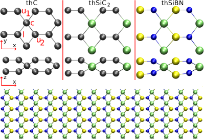
Ram and Mizuseki designed monolayered thC Ram and Mizuseki (2018) by applying a periodic rotation of a C-C dimer (Stone-Wales transformation) to penta-grapheneZhang et al. (2015b). The resulting structure is composed of a periodic arrangement of buckled diamond and hexagons exhibiting dynamical and thermal stability. Two types of C atoms can be differentiated according to the hybridization of their orbitals, namely sp2 and sp3 atoms. Whereas the former are threefold coordinated and their hybridized orbitals form angles of 120∘, similar to graphene, the latter are fourfold coordinated and tend to adopt a tetrahedral geometry (similar to diamond) which is frustrated by the nearly planar configuration of the layer. This leads to a nanostructure that is higher in energy than that of grapheneRam and Mizuseki (2018).
A natural way to alleviate the stress imposed by the frustrated tetrahedral geometry is to substitute the C sp3-hybridized atoms by an atom whose orbitals can either combine yielding a flat configuration or simply be more prone to hybridizing in the sp3 configuration than a C atom. Si exhibits sp3 hybridization in a 2D buckled structure (silicene) Vogt et al. (2012); Guzmán-Verri and Lew Yan Voon (2007), suggesting that a closer-to-tetrahedral arrangement of the Si atomic orbitals is preferred. Also, experimental observations of inclusions of Si atoms in graphene layersZhou et al. (2012); Lopez-Bezanilla et al. (2014) were reported and an sp2d atomic hybridization proposed to explain the flat fourfold Si coordination.
Figure 1 shows the geometry of tetrahexSiC2 (thSiC2) where each Si atom is bonded at first neighbours to four C dimers. This buckled structure exhibits a formation energy 2.15 eV lower than that of the completely flat geometry, suggesting that the sp3 atomic hybridization is preferred over the sp2d. Although the shape of the unit cell and atomic arrangements are the same than in thC, cell vectors increase substantially (18.8% in x and 24.4% in y ) to accommodate the Si atoms, as shown in Table 1. Angles change accordingly as shown in Table 1. As discussed in section III, in addition to Si atom other larger size atoms of group IV are considered in substitution of sp3 hybridized atoms, which yields larger unit cells
III Electronic properties
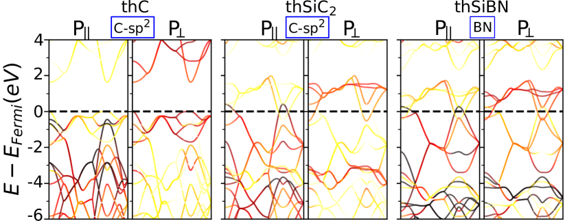
The electronic properties of thC are dominated by the alternating arrangement of hexagons and diamonds that prevents thC from being hyperconjugated. Within the LDA approximation, the band diagram exhibits an electronic band gap at the Fermi level of 1.63 eV, as shown in Figure 2. The exact gap value may depend on the exchange-correlation functional used in the mean-field calculationRam and Mizuseki (2018). A detailed inspection of the contribution of each atomic orbital to the band diagram is conducted with color-weighted bands as plotted in Figure 3. Whereas the fourfold coordinated C atoms barely participate in the low-energy spectrum of thC, the C atoms in sp2 hybridization are responsible for creating the electronic states in the vicinity of the Fermi level. Orbitals contribute differently depending on the their orientation: perpendicular to the plane p⟂ orbitals contribute more than the in-plane orbitals (p||) to both conduction and valence bands.
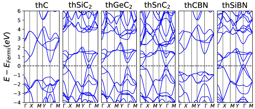
Dimers of p⟂ orbitals in one unit cell are inefficient in forming a chemical bond with neighbouring p⟂ orbitals in the next cell due to the intervening sp3 hybridized C atoms; this results in low-dispersive states at the Fermi level and an insulating band gap. Note an isolated set of four empty conduction bands formed by the lateral overlap of p⟂ orbitals of C sp2 hybridized dimers. Separated from the rest of conduction bands by a 0.9 eV band gap, these bands exhibit a dispersion of 4 eV. As explained below, the shift in energy of these four bands as a result of chemical modification is the key factor that determines the metallic or insulating character of the modified nanostructures.
Si is one position below C in the group IV of the periodic table, namely both atoms share many characteristics such as the same number of valence electrons in a p-orbital: 2p in C atoms and 3p in the Si atoms. Going down in the group IV, heavy metal atoms such Ge and Sn also accommodate four electrons in their outermost 4p and 5p-orbitals respectively. As a result of the increasing difference between the s and p valence orbitals as the size of the atoms increase, -orbitals and -orbitals exhibit a non-negligible mixing in two-dimensional structures based on SiVogt et al. (2012); Grazianetti et al. (2016), GeDávila et al. (2014), and SnZhu et al. (2015). This leads to honeycombed structures where sp3 hybridization is a configuration energetically more stable with respect to all-sp2 graphene which favors the puckering of the layers. With the sp3 hybridization being highly favorable, chemical substitution of sp3 hybridized C atoms by Si, Ge, and Sn atoms is considered in the following as alternative materials.
Figure 1 shows the unit cell of tetrahexSiC2 (thSiC2) where the Si atoms are bonded to four C atoms. The same schematic representation is valid for Ge and Sn substituting atoms, although both the unit cell vectors and the bonding distances increase with increasing group IV atom size. The electronic band diagram of thSiC2 in Figure 2 shows that atomic substitution renders the nanostructure metallic, reduces the dispersion of the conduction bands, and leads to a trivial band inversion by which two of the valence bands become partially empty at the expense of filing partially two conduction bands. The insulating-metallic transition is driven by a shift down in energy of the conduction bands (with respect to thC), that increase their gap to 2 eV with the higher bands, and by a shift up in energy of a set of two occupied bands.
An inspection of the color-weighted bands plotted in Figure 3 shows that the cone-shape band that in thC was totally filled and formed by the in-plane p-orbitals shifts in energy and becomes partially empty in thSiC2. The cone-shape conduction band formed almost exclusively by p⟂-orbitals compensates and produces an electron pocket. Near the zone center two bands play a similar role in the metallicity of the this structure. A charge transfer from p|| to p⟂ orbitals occurs as a result of introducing the Si atom in the nanostructure. Calculations including spin-orbit coupling leave the non-relativistic results unaltered.
Si substitution by Ge atoms leads to thGeC2. A major change introduced in the electronic band diagram when compared to the one of thSiC2 is the semiconducting band gap of 400 meV at the point. Both the shape and dispersion of the conduction bands remain the same. It is interesting to point out that substitution of Si by Ge with no relaxation of the structure leads to a band gap of only 14 meV. (Similarly, substitution of C by Si or Sn shifts conduction bands away from valence bands without opening a band gap). Therefore, the combined effect of atomic substitution and structural relaxation adjust the level of the electronic states and the subsequent creation or disappearance of a band gap.
Substitution of sp3 atoms of thC by Sn atoms yields thSnC2. As in thSiC2 the gap vanishes and a small band inversion at point renders the nanostructure metallic. The electronic gap above the set of four conduction bands also closes and no major variation of the electronic band dispersion is observed.
The non-monotonic trend of gap closing and opening in the sequence C-Si-Ge-Sn is on the first sight surprising, because it runs counter to the usual trend of gap reduction and closing in tetrahedrally coordinated semiconductors as the s-p splitting increases on moving down the periodic table. That trend is in fact present in the manifold of antibonding orbitals which lies above the almost isolated . In the most simplified view the band from three-fold coordinated atoms is sitting rather like an “impurity band” of dimers in a wider gap insulator. The bonding-antibonding manifold is constructed from hybridised four-fold and three-fold ; that gap shrinks monotonously from 6 in thC to around 2 in thSnC2. The band sits at a relatively fixed energy as the larger gap collapses around it.
A common characteristic of the four structures presented above is the isoelectronic character of their constituents. The number of valence electron remain constant and hence the band structures retain a similarity across the substitution series. An additional isoelectronic substitution in thC could change the C atoms in sp2 hybridization. Given that 2D BN is an isomorph of grapheneZeng et al. (2010) able to integrate the layered structure in codoping, the C dimers of the four nanostructures could in principle be substituted by BN dimers. It is worth remembering that BN-based structures are wide-gap insulators due to the polar and ionic character of the B-N bond. 2D hexagonal BN was observed to show metallic behavior when cut along zigzag nanoribbons, which was ascribed to half-metallicity derived from the edge statesZeng et al. (2010).
In Figure 2 the band diagram of tetrahexCBN (thCBN) shows two sets of isolated four bands at both sides of the Fermi level separated by a 1.95 eV wide band gap. The most appealing BN substitution occurs in the dimers of thSiC2, which yields tetrahexSiBN (thSiBN). Figure 2 shows that thSiBN is metallic with a compensated electron-hole pocket similar to that of thSiC2. The dispersive band in the region vanishes, although the cone-shape band remains yielding band inversion in the zone center. An analysis of the weighted bands in Figure 3 shows that the combined p⟂ orbitals of both B and N atoms in the dimers contribute to the conduction bands more than the p|| orbitals, and vice versa for the valence bands. As in the previous structures, the weight of sp3 hybridized atoms in the formation of electronic states in the vicinity of the Fermi level is negligible.
A qualitative Mulliken charge analysis reveals a strong ionic character in multi-atom compounds, specially both thSiC2 and thSiBN. Whereas Si atoms in the former accept 0.1 electrons from the C atoms, in the latter each Si atom behaves as a donor of 0.3 electrons to each BN dimer.
IV Dynamical stability
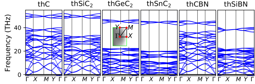
The first report on thCRam and Mizuseki (2018) demonstrated the stability of the monolayer based on a phonon spectrum analysis. The absence of imaginary frequencies indicates dynamical stability since only restoring forces act on an atom that is perturbed a short distance from its equilibrium position. Tiny deviations observed in all structures were minimized within the LDA approximation and very tight convergence criteria in the first-principles calculations. Phonon calculations displayed in Figure 4 shows deviations of 0.75 THz towards imaginary values for one of the acoustic branches starting at point. Whereas a deviation in between two points or at a point of the zone edge could indicate a structural phase transition, phonon softening at the point is indicative of some numerical inaccuracy, and does not demonstrate a structural instability. All compounds presented are dynamically stable and restoring forces are efficient against small perturbation and maintain the structural integrity. Structures formed by substitution of C and Si atoms by Ge and Sn atoms in BN-based structures exhibit instabilities and were discarded in this study.
A total of 32 acoustic and optic modes extend over a frequency range of 40 THz. Separated by a 8 THz gap, four additional optical modes corresponding to in-plane three-fold coordinated atom vibration, lay at 50 THz. This gap increases when the difference of the atomic masses becomes more pronounced in thSiC2 and thSiBN. Also the phonon dispersion lowers with the 32 branches spanning a range of 25 THz.
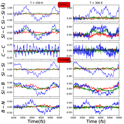
The structural integrity of the layered structures is further verified with molecular dynamic calculations at finite temperature. Starting from the ground-state at T = 150 K and T = 300 K, 5 ps long runs were performed after an initial equilibration time of 1 ps with a 1 fs time-step. From heating at constant temperature the two-dimensional slabs composed of 192 atoms for 5 ps, no structural rearrangement of the atoms was observed. Figure 5 shows relative interatomic distance variations in each orthogonal direction, of nearest Si-Si atoms, and Si-C and C-C dimers. The longer distance variation between atoms is the perpendicular-to-the-plane direction (up to 1 Å), whereas atoms modify their relative distances in the structure plane in a much smaller range. The collective motion of the atoms is a breathing vibration of the nanostructure that expands and compresses, with no large variation of the bonding distance between pairs of atoms. Similar structural stability was observed for the rest of the compounds at finite temperatures. This demonstrates that the structural integrity of the nanostructures is preserved beyond the harmonic approximation, confirming that the compounds are stable up to room temperature.
An alternative arrangements were considered corresponding to a BN dimer followed by a NB dimer along the x-axis after the C bond, and then the opposite arrangement from the parallel BN-C-NB line. That yields two N and two B atoms in front of each other at each side of a C atom, which reduces the distance between two atoms of the same kind, increasing the dipole and destabilizing the structure. The B-C-B and N-C-N distances would be 1.96 Åand 2.06 Å, as opposed to 2.1 Åof B-C-N. In the structures studied here, the shortest distance between two B or two N atoms is 2.5 Å, which helps to balance the negative repulsion between electronegative N atoms. In addition, phonon calculations reveal important softening of some modes as a result of the atomic repulsion.
In a layered structure, the z-axis acoustic modes are relatively soft, and the z-axis lattice constant is potentially temperature-dependent and of course difficult to estimate from numerics with high accuracy. This raises the question about whether the semimetallicity might be dependent on the c-axis lattice constant. The chemical trends elucidated in section III around the closing of the gap between and orbitals is robust. The overlap of the bands is determined by the bandwidth of the dimer band relative to the bonding-antibonding gap. Both of these parameters are established by local in-plane atomic correlations which are not strongly affected by the interlayer distance in the simulation.
V Conclusions
To summarize, a series of 2D materials composed of C and BN dimers woven in a hexagonal-square motif with group IV elements has been studied. Despite the isomorphism and isoelectronic features of the structures, a wide range of electronic behaviors are found. Exchanging C by BN dimers and substituting fourfold coordinated C atoms by isoelectronic Si, Ge, and Sn atoms, insulating-metallic transitions are observed. Whilst the carbon allotrope exhibits an electronic band gap, substitutional of sp3 hybridized C atoms by Si or Sn atoms brings together conduction and valence bands leading to band inversion. Ge atoms yield a similar band structure to the one composed with the previous atoms but exhibit a small band gap. It is remarkable that a 2D nanostructure composed of three different elements exhibits a metallic band structure, since the polar bonds typically lead to gaped electronic band diagrams.
Finally we remark that the electron-hole pockets that form at the fermi surface are very well nested, and the electron gas parameter is about 5 (here is the Fermi momentum and the Bohr radius. Another way to put this is that the Fermi energy of the electron (hole) pockets is around 0.1 eV, which is considerably smaller than the (unscreened) Coulomb energy of order 2 eV. Since the charge transfer from the in plane (hole pocket) to out of plane (electron pocket) will generate a Coulomb interaction that is relatively weakly screened, these semimetals will be good candidates for an excitonic insulator instability where the electron-hole pairs condense.Zhu et al. (1995)
VI Computational Methods
Self-consistent density functional theory (DFT) based calculations were performed within local density approximation (LDA) approachKohn and Sham (1965) for the exchange-correlation functional was used as implemented in the SIESTA codeSoler et al. (2002); Ordejón et al. (1996); García et al. (2020). A double- polarized basis set was used to relax atomic coordinates and compute phonon spectra. Norm-conserving pseudopotentials as implemented in the SIESTA code were employed to represent the electron-ion interaction, so that the pseudopotentials account for the effect of the Coulomb potential created by the nuclei and core electrons creating an effective ionic potential acting on the valence electronsRivero et al. (2015). Atomic positions of the layered materials were fully relaxed with a force tolerance of 0.01 eV/Å. The integration over the Brillouin zone (BZ) was performed using a Monkhorst sampling of 38 42 1 k-points. The radial extension of the orbitals had a finite range with a kinetic energy cutoff of 50 meV. A vertical separation of 35 Å in the simulation box prevents virtual periodic parallel layers from interacting. The force-constant method and the PHONOPY package Togo and Tanaka (2015) were employed for computing phonon spectra. DFT-based molecular dynamic simulations with a Nosé thermostatNosé (1984) were performed in the NVT ensemble for a 441 unit supercells using only the point.
VII Acknowledgments
Los Alamos National Laboratory is managed by Triad National Security, LLC, for the National Nuclear Security Administration of the U.S. Department of Energy under Contract No. 89233218CNA000001. We acknowledge the computing resources provided on Bebop, the high-performance computing cluster operated by the Laboratory Computing Resource Center at Argonne National Laboratory. Work at Argonne is supported by Department of Energy, Office of Science, Basic Energy Sciences Division of Materials Science under Contract No. DE-AC02-06CH11357.
References
- Novoselov et al. (2004) K. S. Novoselov, A. K. Geim, S. V. Morozov, D. Jiang, Y. Zhang, S. V. Dubonos, I. V. Grigorieva, and A. A. Firsov, Electric field effect in atomically thin carbon films, Science 306, 666 (2004), http://science.sciencemag.org/content/306/5696/666.full.pdf .
- Cresti et al. (2008) A. Cresti, N. Nemec, B. Biel, G. Niebler, F. Triozon, G. Cuniberti, and S. Roche, Charge transport in disordered graphene-based low dimensional materials, Nano Research 1, 361 (2008).
- Chang et al. (2013) C.-K. Chang, S. Kataria, C.-C. Kuo, A. Ganguly, B.-Y. Wang, J.-Y. Hwang, K.-J. Huang, W.-H. Yang, S.-B. Wang, C.-H. Chuang, M. Chen, C.-I. Huang, W.-F. Pong, K.-J. Song, S.-J. Chang, J.-H. Guo, Y. Tai, M. Tsujimoto, S. Isoda, C.-W. Chen, L.-C. Chen, and K.-H. Chen, Band gap engineering of chemical vapor deposited graphene by in situ bn doping, ACS Nano 7, 1333 (2013), pMID: 23273110, https://doi.org/10.1021/nn3049158 .
- Gregersen et al. (2018) S. S. Gregersen, J. H. Garcia, A.-P. Jauho, S. Roche, and S. R. Power, Charge and spin transport anisotropy in nanopatterned graphene, Journal of Physics: Materials 1, 015005 (2018).
- Pizzi et al. (2016) G. Pizzi, A. Cepellotti, R. Sabatini, N. Marzari, and B. Kozinsky, Aiida: automated interactive infrastructure and database for computational science, Computational Materials Science 111, 218 (2016).
- Mounet et al. (2018) N. Mounet, M. Gibertini, P. Schwaller, D. Campi, A. Merkys, A. Marrazzo, T. Sohier, I. E. Castelli, A. Cepellotti, G. Pizzi, and N. Marzari, Two-dimensional materials from high-throughput computational exfoliation of experimentally known compounds, NATURE NANOTECHNOLOGY 13, 246+ (2018).
- Lopez-Bezanilla and Littlewood (2015) A. Lopez-Bezanilla and P. B. Littlewood, - band inversion in a novel two-dimensional material, The Journal of Physical Chemistry C 119, 19469 (2015), https://doi.org/10.1021/acs.jpcc.5b04726 .
- Zhang et al. (2015a) S. Zhang, J. Zhou, Q. Wang, X. Chen, Y. Kawazoe, and P. Jena, Penta-graphene: A new carbon allotrope, Proceedings of the National Academy of Sciences 112, 2372 (2015a), http://www.pnas.org/content/112/8/2372.full.pdf .
- Vogt et al. (2012) P. Vogt, P. De Padova, C. Quaresima, J. Avila, E. Frantzeskakis, M. C. Asensio, A. Resta, B. Ealet, and G. Le Lay, Silicene: Compelling experimental evidence for graphenelike two-dimensional silicon, Phys. Rev. Lett. 108, 155501 (2012).
- Zhou et al. (2012) W. Zhou, M. D. Kapetanakis, M. P. Prange, S. T. Pantelides, S. J. Pennycook, and J.-C. Idrobo, Direct determination of the chemical bonding of individual impurities in graphene, Phys. Rev. Lett. 109, 206803 (2012).
- Lopez-Bezanilla et al. (2014) A. Lopez-Bezanilla, W. Zhou, and J.-C. Idrobo, Electronic and quantum transport properties of atomically identified si point defects in graphene, JOURNAL OF PHYSICAL CHEMISTRY LETTERS 5, 1711 (2014).
- Ram and Mizuseki (2018) B. Ram and H. Mizuseki, Tetrahexcarbon: A two-dimensional allotrope of carbon, Carbon 137, 266 (2018).
- de Vasconcelos et al. (2019) F. M. de Vasconcelos, A. G. Souza Filho, V. Meunier, and E. C. Girão, Electronic properties of tetragraphene nanoribbons, Phys. Rev. Materials 3, 066002 (2019).
- Zhang et al. (2015b) S. Zhang, J. Zhou, Q. Wang, X. Chen, Y. Kawazoe, and P. Jena, Penta-graphene: A new carbon allotrope, Proceedings of the National Academy of Sciences 112, 2372 (2015b), https://www.pnas.org/content/112/8/2372.full.pdf .
- Guzmán-Verri and Lew Yan Voon (2007) G. G. Guzmán-Verri and L. C. Lew Yan Voon, Electronic structure of silicon-based nanostructures, Phys. Rev. B 76, 075131 (2007).
- Grazianetti et al. (2016) C. Grazianetti, E. Cinquanta, and A. Molle, Two-dimensional silicon: the advent of silicene, 2D Materials 3, 012001 (2016).
- Dávila et al. (2014) M. E. Dávila, L. Xian, S. Cahangirov, A. Rubio, and G. L. Lay, Germanene: a novel two-dimensional germanium allotrope akin to graphene and silicene, New Journal of Physics 16, 095002 (2014).
- Zhu et al. (2015) F.-f. Zhu, W.-j. Chen, Y. Xu, C.-l. Gao, D.-d. Guan, C.-h. Liu, D. Qian, S.-C. Zhang, and J.-f. Jia, Epitaxial growth of two-dimensional stanene, NATURE MATERIALS 14, 1020+ (2015).
- Zeng et al. (2010) H. Zeng, C. Zhi, Z. Zhang, X. Wei, X. Wang, W. Guo, Y. Bando, and D. Golberg, “white graphenes”: Boron nitride nanoribbons via boron nitride nanotube unwrapping, Nano Letters 10, 5049 (2010), pMID: 21028887, https://doi.org/10.1021/nl103251m .
- Zhu et al. (1995) X. Zhu, P. B. Littlewood, M. S. Hybertsen, and T. M. Rice, Exciton condensate in semiconductor quantum well structures, Phys. Rev. Lett. 74, 1633 (1995).
- Kohn and Sham (1965) W. Kohn and L. J. Sham, Self-consistent equations including exchange and correlation effects, Phys. Rev. 140, A1133 (1965).
- Soler et al. (2002) J. M. Soler, E. Artacho, J. D. Gale, A. García, J. Junquera, P. Ordejón, and D. Sánchez-Portal, The siesta method for ab initio order- n materials simulation, Journal of Physics: Condensed Matter 14, 2745 (2002).
- Ordejón et al. (1996) P. Ordejón, E. Artacho, and J. M. Soler, Self-consistent order-n density-functional calculations for very large systems, Phys. Rev. B 53, R10441 (1996).
- García et al. (2020) A. García, N. Papior, A. Akhtar, E. Artacho, V. Blum, E. Bosoni, P. Brandimarte, M. Brandbyge, J. I. Cerdá, F. Corsetti, R. Cuadrado, V. Dikan, J. Ferrer, J. Gale, P. García-Fernández, V. M. García-Suárez, S. García, G. Huhs, S. Illera, R. Korytár, P. Koval, I. Lebedeva, L. Lin, P. López-Tarifa, S. G. Mayo, S. Mohr, P. Ordejón, A. Postnikov, Y. Pouillon, M. Pruneda, R. Robles, D. Sánchez-Portal, J. M. Soler, R. Ullah, V. W.-z. Yu, and J. Junquera, Siesta: Recent developments and applications, The Journal of Chemical Physics 152, 204108 (2020), https://doi.org/10.1063/5.0005077 .
- Rivero et al. (2015) P. Rivero, V. Manuel García-Suárez, D. Pereñiguez, K. Utt, Y. Yang, L. Bellaiche, K. Park, J. Ferrer, and S. Barraza-Lopez, Systematic pseudopotentials from reference eigenvalue sets for dft calculations: Pseudopotential files, Data in Brief 3, 21 (2015).
- Togo and Tanaka (2015) A. Togo and I. Tanaka, First principles phonon calculations in materials science, Scr. Mater. 108, 1 (2015).
- Nosé (1984) S. Nosé, A unified formulation of the constant temperature molecular dynamics methods, The Journal of Chemical Physics 81, 511 (1984), https://doi.org/10.1063/1.447334 .