ANA-LARG-2019-01-PAPER.bib \addbibresourcebib/ATLAS.bib \addbibresourcebib/CMS.bib \addbibresourcebib/ConfNotes.bib \addbibresourcebib/PubNotes.bib \AtlasTitleThe Phase-I Trigger Readout Electronics Upgrade of the ATLAS Liquid Argon Calorimeters \AtlasAbstractThe Phase-I trigger readout electronics upgrade of the ATLAS Liquid Argon calorimeters enhances the physics reach of the experiment during the upcoming operation at increasing Large Hadron Collider luminosities. The new system, installed during the second Large Hadron Collider Long Shutdown, increases the trigger readout granularity by up to a factor of ten as well as its precision and range. Consequently, the background rejection at trigger level is improved through enhanced filtering algorithms utilizing the additional information for topological discrimination of electromagnetic and hadronic shower shapes. This paper presents the final designs of the new electronic elements, their custom electronic devices, the procedures used to validate their proper functioning, and the performance achieved during the commissioning of this system. \AtlasJournalJINST \hypersetuppdftitle=LAr document,pdfauthor=The ATLAS LAr Collaboration
1 Introduction
During the second Large Hadron Collider (LHC) Long Shutdown (LS2), the Liquid Argon (LAr) calorimeters of the ATLAS experiment have been equipped with new trigger readout electronics [phase1tdr], which provides digital information to the ATLAS trigger system [TRIG-2011-02]. The purpose of this so-called Phase-I\xspaceupgrade is to enhance the physics reach of the experiment during the upcoming operation at increasing LHC luminosities. ATLAS ran in the Run 2\xspacedata taking period (years 2015–2018) at a typical maximum instantaneous luminosity of \highLand with an average mean number of proton-proton interactions of [ATLAS-CONF-2019-021]. During Run 3\xspace(years 2022–2025) the instantaneous luminosity was originally expected to increase to a peak value of \highL, with [phase1tdr]. The updated LHC plan for Run 3\xspacetargets a beam intensity increase of 50% compared to Run 2\xspacewith a luminosity leveled to \highLover periods up to 12 hours. The center-of-mass energy will also be raised from \sqs=\SI13\tev to \SI13.6\tev. These changes will result in an overall detector occupancy increase, while the first level trigger (L1) bandwidth will remain at \SI100kHz during Run 3\xspace. If the currently used LAr trigger readout system, referred to as legacy trigger readout in the following, were to remain unchanged, the transverse energy (\ET) trigger thresholds would need to be raised, degrading the physics performance. To avoid this efficiency loss and enhance the physics reach of the experiment in Run 3\xspaceand beyond, the new system installed during LS2 increases the readout granularity by up to a factor of ten: instead of summing the \ETof calorimeter cells in areas as small as to form the so-called Trigger Towers of the legacy readout, additional lateral and longitudinal segmentation is introduced to form smaller clusters called Super Cells. Trigger Towers are typically split longitudinally into four layers, and some layers are split laterally along into four strips each. One Super Cell can thus cover an area as small as , depending on which longitudinal layer it is located in. In addition, the precision and range of the \ETmeasurement is also increased. Consequently, the background rejection at trigger level is improved due to better filtering algorithms being possible already at L1, based on topological discrimination between electromagnetic shower shapes and hadronic activity. In particular, the resulting electron, photon and tau lepton identification is more efficient. Furthermore, thanks to more advanced reconstruction algorithms and better pile-up subtraction techniques, the energy resolution for electromagnetic, jet and missing \ETobjects is improved, leading to a sharper rise of the per-event trigger efficiency toward its plateau value.
The Phase-I\xspaceupgrade project is part of a broad upgrade program of the LAr calorimeters through the lifetime of the LHC and is fully compatible with the future Phase-II\xspaceupgrade program of the ATLAS experiment planned for the third Long Shutdown (LS3) in 2026–2028.
This paper presents the new system, initially proposed in Reference [phase1tdr] and installed during LS2, together with its performance. The final designs of the new electronic boards and their Application-Specific Integrated Circuits (ASICs) are described as well as the procedures used to validate their proper functioning. The basic performance achieved during the commissioning of this system is also presented. In \Sect2, the legacy readout electronics is briefly recapitulated and the new trigger readout electronics is introduced, as are the new data paths. The new electronics installed on the ATLAS detector (Front-End) and off the detector (Back-End) is described in \Sects3LABEL:sec:be, respectively. Finally, the integration tests performed to validate the full chain of this new readout electronics are reported in \SectLABEL:sec:integration before the conclusions are presented in \SectLABEL:sec:conclusion.
2 Overview of the LAr readout electronics
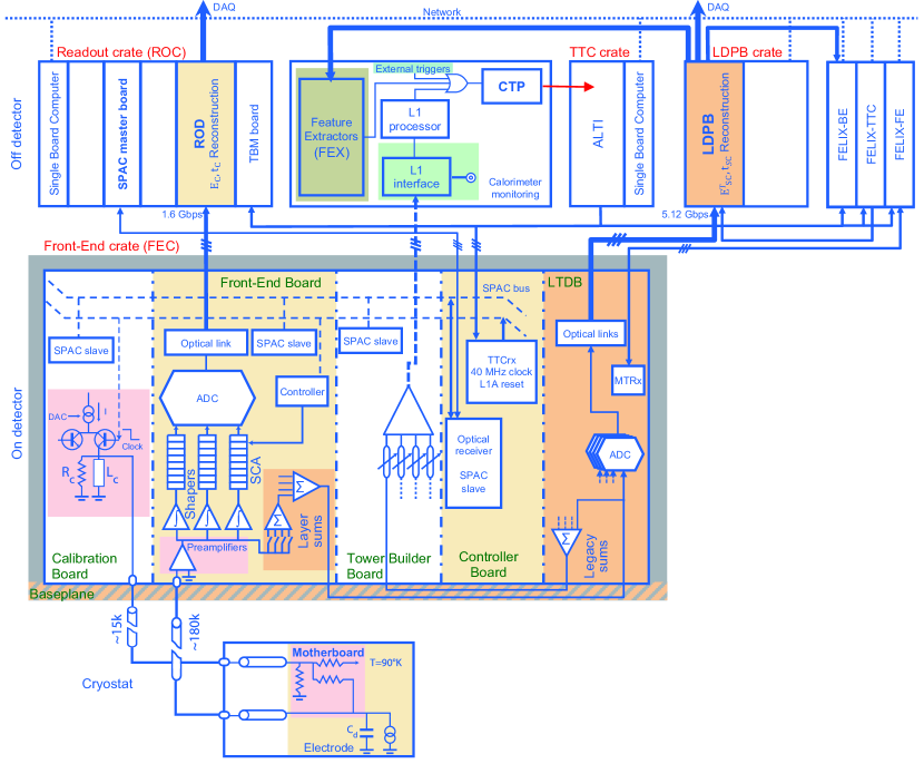
The readout electronics of the LAr calorimeters is designed to record energies approximately ranging from \SI50\MeV to \SI3\TeV, measured in 182418 calorimeter cells. The energy resolution of the calorimeter for electromagnetic showers can be written as , with an intrinsic sampling term that is typically 10–11% [TestBeam2006, TestBeam2007], a constant term that is 1–2% [PERF-2017-03], and a noise term that is 10–\SI600\mev without pile-up contribution [LArElecPerf2010] and is expected to be \SI30\mev–\SI3\gev in Run 3\xspacepile-up conditions [phase1tdr], depending on the pseudorapidity region considered (up to ). The triangular pulse coming from the ionization in a LAr cell is shaped into a bipolar pulse that is sampled at \SI40MHz. The digitized samples are read at the L1 trigger rate, that can go up to \SI100kHz. The LAr calorimeter system is composed of four different components: the electromagnetic barrel (EMB) and end-caps (EMEC), both referred to as EM calorimeters; the hadronic end-cap (HEC); and the forward calorimeter (FCal). These components are divided in two sides, A and C, oriented respectively along the positive and negative -axis of the experiment. The LAr readout electronics is divided into a Front-End and a Back-End system, both interconnected by cables and optical fibers as shown in Figure 1.
The Front-End system is composed of 58 Front-End Crates (FECs), each hosting at most two baseplanes which interconnect the following legacy system boards:
- Front-End Boards (FEBs):
-
process typically 128 channels, each in a specific longitudinal layer of the calorimeter. They amplify, shape, sample and digitize the ionization signals and transmit them to the Back-End readout. The analog sums needed for the trigger system are also prepared by the Linear Mixers and the Layer Sum Boards (LSBs), both hosted on the FEBs. The Linear Mixer electronics is part of the shaper chip located on the FEB motherboard, while the LSB is a plug-in card connected to the Linear Mixer.
- Tower Builder Boards (TBBs):
-
form the legacy Trigger Towers from the analog sums provided by the LSBs over the FEC baseplanes. The Trigger Tower analog signals are sent to the L1 trigger system via copper cables. In the HEC and FCal no further sums need to be produced after the LSB. Therefore, Tower Driver Boards (TDBs) are used in place of TBBs.
- Calibration Boards:
-
inject current calibration pulses whose shape is close to the pulse generated from the LAr ionization signal.
- Controller Boards:
-
receive the configuration and monitoring commands from the Serial Protocol for Atlas Calorimeter [SPAC] (SPAC) masters installed in the Back-End Readout Crates. Controller boards receive also the Timing Trigger and Control [TTC] (TTC) signals coming from the Back-End TTC crates. They distribute the SPAC and TTC commands to the other legacy boards in the FEC.
Some FECs also host monitor boards transmitting the information from the sensors measuring possible mechanical stresses of the detector and the LAr temperature and purity. Another function of some of the monitor boards is to measure the status of the FECs’ low-voltage power supplies. Each electronic board in a FEC is conductively cooled using two aluminium plates placed on each side of the board. These aluminium plates are part of a leak-less water cooling system.
On the Back-End side, two legacy systems are present:
- Readout Crates (ROCs):
-
Versa Module Eurocard (VME) crates hosting Readout Driver boards (RODs) that read the Analog-to-Digital Converter (ADC) data sent by the FEBs and compute energy () and time () for each cell signal at the L1 trigger rate. The ROCs also house the SPAC master boards and the Trigger Busy Modules (TBMs). The latter collect the busy signals from the RODs and distribute the TTC signals.
- TTC crates:
-
VME crates containing the modules that receive the TTC commands from the ATLAS Central Trigger Processor (CTP) system or generate locally these commands and transmit them to the other LAr boards.
The LAr electronics upgrade extends the legacy system with new Front-End components, sending the Super Cells’ digital data to new Back-End components, which compute and transmit the Super Cells’ \ETto the new trigger system. The architecture as of Run 3\xspaceis illustrated in Figure 1. This new LAr trigger readout system is composed of new Layer Sum Boards providing the analog sums for the higher trigger readout granularity; new baseplanes to route the increased number of analog signals and host the new LAr Trigger Digitizer Boards (LTDBs) that digitize the Super Cell analog signals at \SI40MHz and provide the legacy sums for the TBBs; and new Back-End boards, the LAr Digital Processing Blades (LDPBs), that read the Super Cell ADC signals from the LTDBs, compute the Super Cells’ \ETand send them to the new L1 trigger system. This new trigger system comprises a set of Feature EXtractors (FEX) with three subsystems targeting electromagnetic (eFEX), jet (jFEX) and global (gFEX) features [ATLAS-TDR-23]. The choice to convert the Super Cells’ energy to \ETat the LDPB level was made to simplify the LTDB design. The LDPB is built in Advanced Telecommunications Computing Architecture (ATCA) format and comprises one ATCA carrier blade named LAr Carrier (LArC) and up to four Advanced Mezzanine Cards (AMCs) called LAr Trigger prOcessing MEzzanines (LATOMEs). The hardware control and monitoring of each blade proceeds via an Intelligent Platform Management Controller (IPMC) plugged into the LArC. In total, 124 LTDBs are installed on the 114 new baseplanes. Furthermore, 30 LDPBs corresponding to 30 LArCs and 116 LATOMEs, are installed in three ATCA shelves placed in one 19-inch rack. This new LAr system uses also three separate Front-End LInk eXchange (FELIX) [felix] systems, comprising a total of 30 FELIX boards.
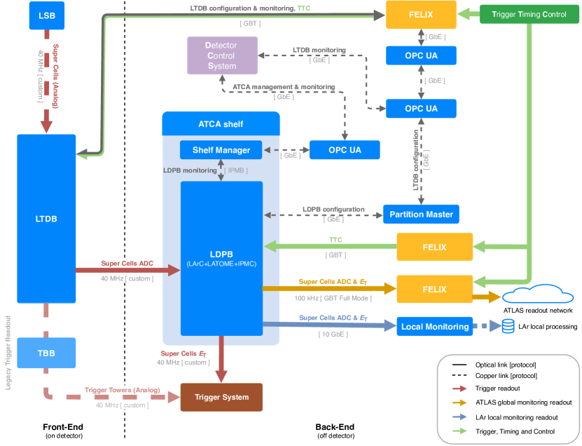
The new trigger readout path is illustrated in Figure 2 with solid red arrows. In order to ease the new system commissioning and have a fallback solution in case of unforeseen issues, the legacy trigger readout is kept functional since the LTDB sends the re-summed analog signals to the TBB, which will remain in operation during at least the initial phase of the LHC Run 3\xspace. The legacy trigger readout path is illustrated in Figure 2 with dashed red arrows.
Several other data paths are present in the system. A global monitoring path utilizes a Full Mode [felix] data link between each LATOME and the FELIX system that connects to the ATLAS main data readout (path in orange arrows in Figure 2). Its purpose is to verify that the \ETsent to the trigger system is correct, by reading the Super Cell ADC data and the \ETvalues for all events selected by the first level trigger accept signal (L1A). Thus, this readout allows a recomputation of the calculation performed in the LATOME boards.
A similar monitoring path utilizes the 10 Gigabit Ethernet (GbE) interface of the ATCA shelf that hosts the LDPBs (blue arrow in Figure 2). This readout is not connected to the ATLAS main readout but is used by a processing server specific to the LAr system. It enables a more flexible and localized monitoring to readout Super Cell ADC data and \ETat the L1A signal rate or optionally at any other rate, independently of the constraints present in the ATLAS main data readout in terms of bandwidth and event rate.
The whole system is synchronized with the TTC signals (green arrows in Figure 2). These signals provide the \SI40MHz LHC reference clock, the L1A, the Bunch Counter Reset (BCR), the Event Counter Reset (ECR) and the Trigger Type commands. The BCR corresponds to the LHC orbit frequency and enables the determination of the collision time of an event via its Bunch Crossing IDentifier (BCID). The ECR is used to compute an event identifier and the Trigger Type records which subsystem issued the L1A. The TTC signals are transmitted to LTDB and LDPB through FELIX systems with Gigabit Transceiver (GBT) [GBT1, GBT2] links.
The configuration of the LTDB and LDPB hardware proceeds via a ”Partition Master” PC. This computer is connected to LTDBs in three stages: two Open Platform Communications Unified Architecture (OPC UA) servers and a FELIX system, connected to LTDBs via GBT links. The first OPC UA server takes care of the LTDB configuration command generation, according to the run control commands received from the Partition Master. The second OPC UA server packs these specific commands to follow the GBT protocol. The Partition Master connection to the LDPB is made directly via a \SI1GbE interface.
A Detector Control System [DCS] (DCS) handles the hardware monitoring: it ensures that the hardware is operated under safe conditions and provides basic safety mechanisms in case of failure. The connection to the LTDB is made with a part of the same OPC UA and FELIX chain used for the configuration. The LDPB is connected to the DCS via an OPC UA server and the ATCA shelf manager, interfaced to the IPMC on the LDPB via an Intelligent Platform Management Bus (IPMB).
Some differences exist in the signal processing between the main and trigger readout systems: the analog signal processing in the main readout comprises pre-amplification followed by shaping performed in three different gain scales, such that three overlapping gains are obtained with a ratio of about 10. The bipolar shape is created with a time constant of \SI13ns. The samples stored by the Switched Capacitor Array (SCA) analog pipeline chip are digitized by a 12-bit ADC and sent to the Back-End system via a 1.6 Gigabit per second (Gbps) optical link. In the trigger readout, the analog processing has a similar shaping with only one gain scale, but with a special conditioning described in \SectLABEL:sssec:ltdb-motherboard. The Super Cells’ digital samples generated in the LTDBs are sent to the Back-End system with a \SI5.12Gbps optical link. While in the main readout the RODs compute the cell energies and signal times at the L1A rate (up to \SI100kHz), the LDPBs of the trigger readout compute the Super Cell transverse energies () and signal times () at the LHC collision rate (\SI40MHz).
The new trigger readout aims to have an Integral Non-Linearity (INL) for each Super Cell channel below \SI1% with a Super Cell energy computation precision below \SI250\mev. Even under high pile-up data taking conditions, this computation must remain unbiased.
In the following, the new hardware, as well as the procedures carried out to validate its functionalities, are described in detail.
3 New Front-End electronics
3.1 Baseplanes
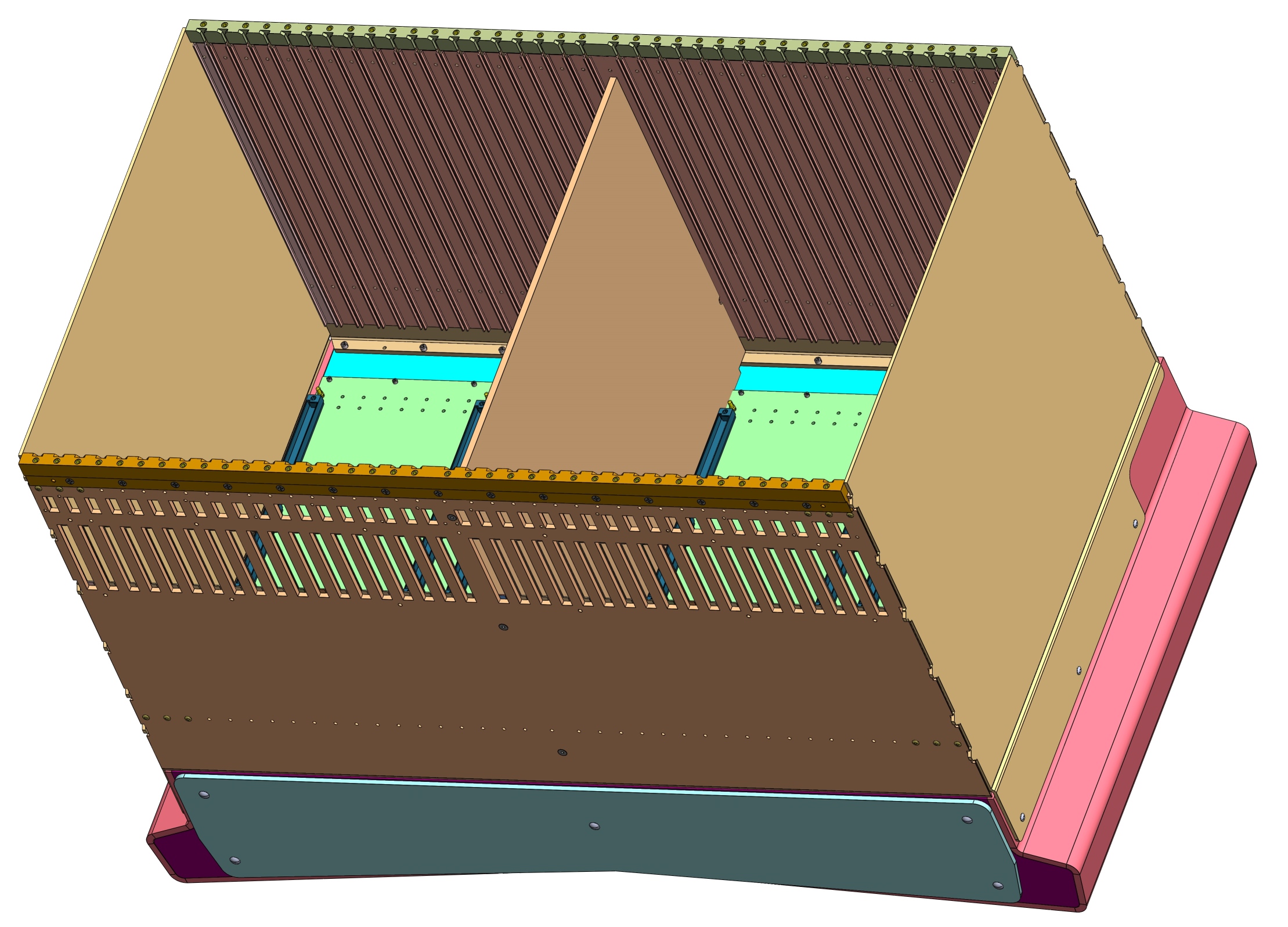
At each end of the barrel cryostat 32 calorimeter signal feedthroughs [Axen:2005vb] are installed, distributed around the cylindrical periphery at nearly uniform angles. Each of the two end-cap cryostats has 25 signal feedthroughs distributed around the far end (from the collision point) of its periphery. Each feedthrough with cold and warm flanges connected via vacuum cables is made up of four pin carriers. Each pin carrier has either seven or eight connectors and each connector has 64 signal pins. A pedestal spans two adjacent feedthroughs and a FEC is mounted on each pedestal. Each FEC is divided into two halves with a baseplane installed in each half for almost all of the crates, see Figure 3. For each connector in a pin carrier a flex ribbon cable carries 64 signals from the feedthrough to a connector on the back side of the baseplane. The pins in this connector extend through to the front side of the baseplane. A FEB has two 64-pin signal connectors and this board, mounted in a FEC, plugs into the baseplane. Between the two signal connectors on each FEB is a third 64-pin connector, which returns analog trigger signals to the baseplane where they are routed to trigger-handling boards, also plugged into the baseplane.
For the Phase-I upgrade, new baseplanes are required (1) to accommodate the finer trigger segmentation, (2) to make room for the LTDBs (Section 3.3), and (3) to maintain the legacy Level-1 trigger system. The new mezzanine LSBs (Section 3.2), mounted on the existing FEBs, provide more analog signals than before onto the baseplanes, which are now routed to both the LTDBs and to the existing TBBs or TDBs requiring additional signal layers on the baseplane Printed Circuit Boards (PCBs). Because the LTDB baseplane connectors are wider than those for the other boards plugged into the baseplane, there is no space next to an LTDB for the Radio Frequency (RF) shields which protect the small-signal inputs to the FEBs from extraneous noise. This requires, in some cases, additional slots and/or significant re-arrangement of the baseplane slot assignments, as well as thicker baseplane PCBs, whose thickness is highly constrained by the existing size of the FEC and FEBs. Table 1 gives an overview of the physical dimensions of the various baseplane types.
| \toprule | EMB |
|
|
HEC |
|
|
||||||||
| \midrulePCB layers | 12 | 12 | 14 | 12 | 16 | 16 | ||||||||
| Length [mm] | 388.00 | 388.00 | 522.73 | 260.00 | 450.60 | 490.00 | ||||||||
| Width [mm] | 415.00 | 415.00 | 415.04 | 415.00 | 406.40 | 406.40 | ||||||||
| Thickness [mm] | 2.40 | 2.40 | 2.36 | 2.36 | 2.36 | 2.36 | ||||||||
| # on detector | 64 | 32 | 8 | 8 | 1 | 1 | ||||||||
| \bottomrule |
The new EMB baseplane has the same number of slots (19) as the original baseplane. Space for the single new LTDB comes from a previously unallocated slot at one end of the FEC. Some FEBs have been shifted by one slot to allow the LTDB to sit in the middle slot of the baseplane next to the TBB (see Figure 4). The flex ribbon cable connections underneath the baseplane are then also shifted by the same amount.
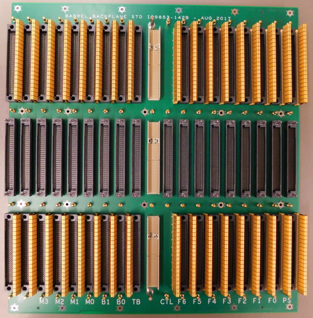

The EMEC crates house two different types of baseplanes. The EMEC standard crate has baseplanes similar to the EMB but with one fewer FEB, leaving a slot for an additional monitor board. The EMEC special crate has one baseplane for the EMEC and another for the HEC. The EMEC special baseplane has two LTDBs and it extends well beyond the center of the crate. The HEC baseplane in the other side of the crate consequently has room for only 13 slots rather than the normal 19 slots of the EMB baseplanes and the EMEC standard baseplanes. An overview of the different boards which plug into the various baseplane types can be found in Table 2.
| \toprule | EMB |
|
|
HEC | FCAL | ||||
|---|---|---|---|---|---|---|---|---|---|
| \midruleFEBs | 14 | 13 | 17 | 6 | 14 | ||||
| LTDBs | 1 | 1 | 2 | 1 | 2 | ||||
| TBBs | 1 | 1 | 3 | 0 | 0 | ||||
| TDBs | 0 | 0 | 0 | 2 | 2 | ||||
| Calibration | 1 | 1 | 2 | 1 | 1 | ||||
| Controller | 1 | 1 | 1 | 1 | 1 | ||||
| Monitor | 1 | 2 | 0 | 0 | 1 | ||||
| Low Voltage Power | 0 | 0 | 0 | 2 | 0 | ||||
| \midruleTotal | 19 | 19 | 25 | 13 | 21 | ||||
| \bottomrule |
The original FCal baseplanes had 19 slots, each fitting within one-half of a FEC. The other half was used for devices which monitor the status of the cryostats. The new FCal baseplanes each have two LTDBs and the baseplanes extend two (three) slots into the now unused other half crate for the A-end (C-end). Integrated into each new FCal baseplane are traces carrying pulses from the calibration board through attenuating injection resistors (surface mounted on the backside of the baseplane) to those pins on the baseplane connectors which carry FEB signals.
Prototype and production baseplanes were subjected to a series of tests. For those connector pins which are specified to be grounded, the impedance to ground was confirmed to be consistent with zero. Likewise, connector pins which are not specified to be grounded were also checked. The impedance of traces on the baseplanes was measured with a time-domain reflectometer. Continuity between trace ends was compared with the net lists. These mapping tests were then compared with independent LTDB mapping requirements. Signal integrity on the traces and cross-talk between near-by traces were measured with a pulser and oscilloscope to verify that they met specifications. In the case of the FCal baseplanes, the calibration injection resistors were all measured for correct values. All baseplanes were shown to meet the specifications.
3.2 Layer Sum Boards
In the LAr trigger readout, the first level of summing is provided by the Linear Mixer, which sums over four channels in azimuth with different gains in different regions of . The upgrade to the trigger branch begins with the ouput of this signal. The LSB is a plug-in card for the FEB that performs a second level of summing of the analog signals [Buchanan:2008zza]. There are two LSBs mounted on each FEB. For the Phase-I\xspaceupgrade, the new LSB output provides signals for the finer granularity Super Cells in the front and middle layers, while retaining the signals needed for the legacy trigger path elsewhere. Six main types of new LSBs have been produced:
- S2x8
-
The basic circuit on the board performs an analog sum of two input channels from the Linear Mixer. There are eight copies of this circuit on each LSB. There are 896 boards of this type required for the EMB and 192 for the EMEC, with 288 reused from the original construction.
- S2x8D
-
S2x8 LSBs were already used in the back layer of the EM calorimeters. For Phase-I\xspace, this output signal must be sent to both the new LTDB and the legacy TBB. A simple splitter is added to the S2x8 in order to produce this dual output. There are 128 boards of this type required for the EMB and 160 for the EMEC.
- S1x16LN
-
This LSB has no summing function and only serves as a line driver for the Linear Mixer signal. There are sixteen copies of this circuit on each LSB. There are 448 boards of this type required for the EMB and 544 for the EMEC.
- S1x12+S6x2
-
For the front section of the EMEC in the range , the output from the shapers covers the area . These are sent individually to the LTDB, while sums of six inputs are sent to the TBB. There are 128 boards of this type required for the EMEC.
- S2x6D+S1x4
-
At the end of the EM Barrel (), each LSB must handle four signals originating from the middle layer and 12 signals from the back layer. The signals from the back layer are summed and handled with the same circuitry as the S2x8D and sent to the LTDB and TBB, while the four signals from the middle are just passed directly to the LTDB as in the S1x16LN circuit. There are 128 boards of this type required for the EMB.
- FCal
-
All the LSBs above form an unweighted sum of cells in a narrow region of , while in the FCal, one must perform a sum over a relatively wide range in pseudorapidity, over which the conversion factor from energy to transverse energy varies significantly. For this reason, the inputs to be summed on the FCal LSBs are weighted to perform the conversion to transverse energy before summing. This leads to a large variety of LSBs, which, within a given FCal module, differ only by the weighting resistor values. All 56 FCal LSBs were replaced by the new design.
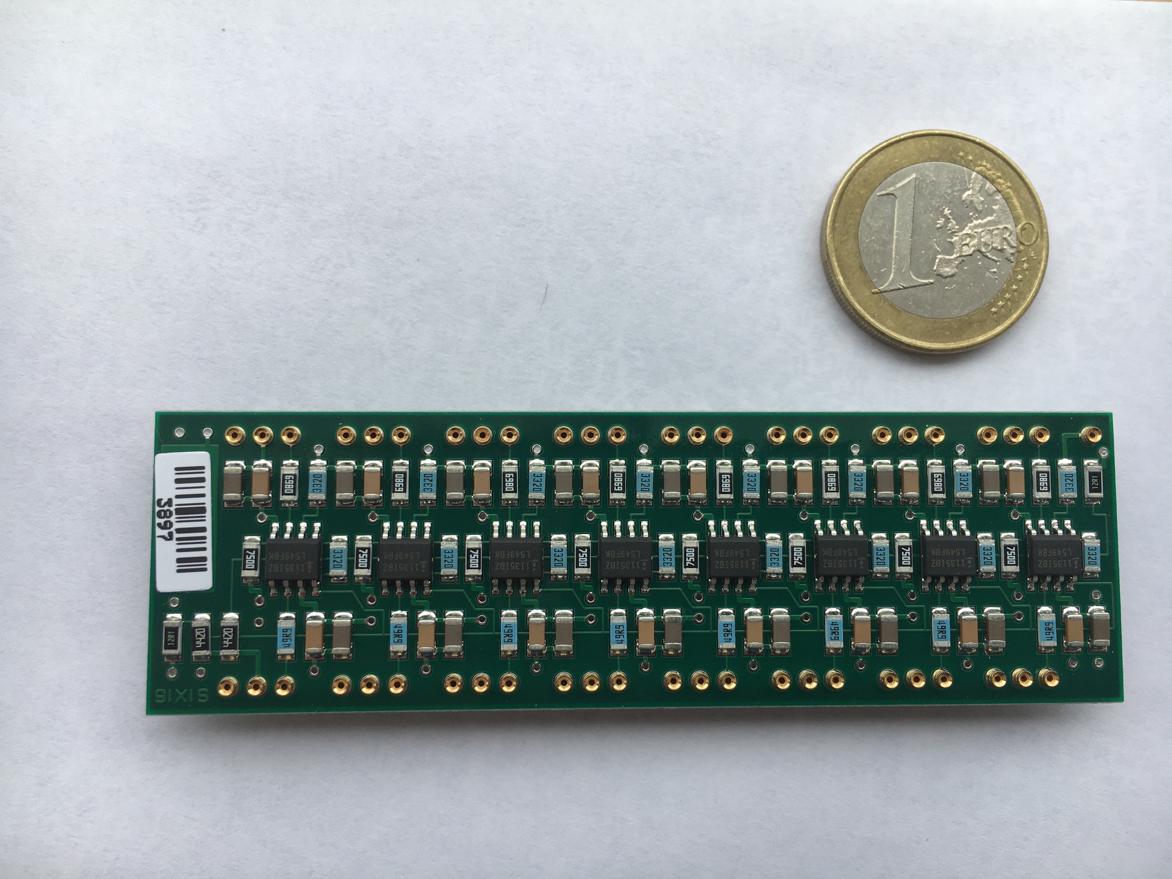
The technical specifications for all the boards are that the gain should not vary by more than 2% from nominal, the summing amplifier INL should be ¡ 1%, and the Direct Current (DC) offset should be ¡ 2% of the maximum output voltage. All boards were tested before and after a week-long burn-in. About 99% passed the specification and were delivered to CERN. As the replacement of the baseplanes required that all electronics in the FECs be disconnected and removed, all FEBs were brought to a surface laboratory. Here, the FEBs were “opened” (i.e. the cooling plates dismounted) and the LSBs replaced by the new boards. Figure 5 shows a photo of an example LSB.
3.3 LAr Trigger Digitizer Boards
An LTDB processes and digitizes up to 320 Super Cell signals (“channels”) and transmits them via optical links to the Back-End, while also providing summed analog legacy signals for the TBB via the new baseplanes. The following sections describe the key ASICs for digitization and optical transmission, the motherboard that houses them, the mezzanine card providing the power, quality assurance and control for the assembled system as well as considerations on compatibility with the Phase-II\xspaceupgrade.
3.3.1 Analog-to-Digital Converter
A custom, quad-channel, pipeline ADC was designed to process the shaped analog signals from the LAr calorimeter Super Cells. These signals are continuously sampled and digitized at 40 Megasamples per second. To digitize the energy of the trigger signals, the ADC has a dynamic range of approximately 12 bits (after calibration) with a required precision of at least 10 bits [phase1tdr]. Each ADC consumes \SI45mW per channel and has a latency of less than \SI125ns, meeting the power and latency budgets at the system level of less than \SI145mW per channel and \SI200ns, respectively.
Radiation tolerance is a key requirement for the ADC, as it is for all devices located on-detector and within the substantial radiation field. The device must operate reliably through the remaining LHC run, as well as the High Luminosity LHC (HL-LHC) runs, with a total expected integrated luminosity of \SI3000