Broadband polarization insensitivity and high detection efficiency in high-fill-factor superconducting microwire single-photon detectors
Abstract
Single-photon detection via absorption in current-biased nanoscale superconducting structures has become a preferred technology in quantum optics and related fields. Single-mode fiber packaged devices have seen new records set in detection efficiency, timing jitter, recovery times, and largest sustainable count rates. The popular approaches to decreasing polarization sensitivity have thus far been limited to introduction of geometrically symmetric nanowire meanders, such as spirals and fractals, in the active area. The constraints on bending radii, and by extension, fill factors, in such designs limits their maximum efficiency. The discovery of single-photon sensitivity in micrometer-scale superconducting wires enables novel meander patterns with no effective upper limit on fill factor. This work demonstrates simultaneous low-polarization sensitivity () and high detection efficiency ( with confidence at counts per second) across a nm bandwidth centered at 1550 nm in 0.51 wide microwire devices made of silicon-rich tungsten silicide, with a fill factor in the active area. These devices boasted efficiencies of 96.5-96.9% 0.5% at counts per second for 1550 nm light.
I Introduction
Superconducting nanowire single-photon detectors (SNSPDs) are a premier technology for applications that require fast, high-efficient detection and high-timing resolution. Their utility spans such diverse areas as fundamental research Hochberg et al. (2019), communications Mao et al. (2018); Chen et al. (2020), metrology Slussarenko et al. (2017), remote sensing Zhu et al. (2017), materials research Chen et al. (2018), and astronomy Zhuang, Zhang, and Shapiro (2018); Khabiboulline et al. (2019). Such detectors in single-mode fiber-packaged form have been fruitfully employed in several ground-breaking quantum-optics experiments Shibata, Honjo, and Shimizu (2014); Dixon et al. (2014); Shalm et al. (2015); Takesue et al. (2015); Najafi et al. (2015); Jin et al. (2015); Weston et al. (2016); Saglamyurek et al. (2016). Within the past five years, fiber-packaged SNSPDs have seen new records set in such diverse figures-of-merit as system-detection efficiency (SDE) Reddy et al. (2020); Hu et al. (2020); Chang et al. (2021), timing jitter Korzh et al. (2020), and low dark counts Shibata et al. (2017). The field is making advances towards joint high performance in multiple metrics simultaneously. One such goal is high SDE coupled with low polarization sensitivity.
We define polarization sensitivity (PS) for a device as the ratio of the maximum to minimum SDE across all input polarization states of photons. Traditional fiber-coupled SNSPDs have consisted of nanowire meanders covering the active area (where photons are expected to be absorbed) in a zig-zag pattern. The geometry forms a grating-like structure of parallel strips of superconductor spaced by a dielectric. Consequently, SNSPDs have inherently possessed a non-unity PS Anant et al. (2008); Redaelli et al. (2016); Zheng et al. (2016); Redaelli et al. (2017). While such meanders allow for unity PS at a specific wavelength via cleverly engineered anti-reflection coatings Reddy et al. (2019), reliable unity-PS across significant bandwidths has remained unrealized in high-efficiency devices. Applications that require high efficiency and throughput Shalm et al. (2015); Ghafari et al. (2019); Shalm et al. (2021) often use polarization controllers before directing light to the detectors, which is a significant source of loss. High-SDE devices with either unity, or infinite PS (meaning no sensitivity to one polarization) would mitigate such issues. Such detectors would also close a security loophole in standard phase-encoding quantum-key distribution implementations Wei et al. (2019).
Historical approaches to achieving unity PS have sought to spatially symmetrize the nanowire-meander geometries. PS values of 1.02-1.04 have been measured in spiral SNSPDs since 2008 Dorenbos et al. (2008); Henrich et al. (2013); Huang et al. (2017) with limited SDE. In 2012, Verma et al. fabricated a two-layer 3D-SNSPD with perpendicularly oriented meanders, and showed a PS of 1.02 with an SDE of 87.7% Verma et al. (2012). Space-filling fractals such as Sierpinski or Hilbert curves have also been studied as a means of introducing discrete rotational symmetries into nanowire meanders Gu et al. (2015). The fractal approach has seen steady improvement Chi et al. (2018); Meng et al. (2020a), and has recently realized a PS of at 91% efficiency Meng et al. (2020b). The introduction of turns and hairpin bends in the active area renders the outer-radii regions of such fractal-meander nanowires relatively insensitive to photons Clem and Berggren (2011); Meng et al. (2020b), thus limiting their efficiency. Other innovations that do not symmetrize the meander geometry have focused on high-refractive index dielectric media surrounding the nanowires to reduce the effective grating-index contrast Redaelli et al. (2016); Zheng et al. (2016); Redaelli et al. (2017); Xu et al. (2017); Mukhtarova et al. (2018). Alternatively, instead of minimizing PS, deliberate introduction of grating-like asymmetries in the optical stack using dielectric or metal slots to maximize PS have also been considered Xu et al. (2018); Li and Jiao (2019).
The year 2020 witnessed several observations of micrometer-wide superconducting structures being sensitive to single photons when current biased. While such scales were trivial for higher-energy photons such as X-rays Yang et al. (2021), Korneeva et al. showed the first such instance for near-infrared (IR) photons Korneeva et al. (2020). Specifically, they observed that 3.3 nm thick, 2 wide molybdenum silicide (MoSi) microstrips could detect photons of wavelength 1 . Chiles et al. modified their tungsten silicide (WSi) recipe to increase the stoichiometric proportion of silicon, and demonstrated near-IR photon sensitivity in wires as wide as 4 Chiles et al. (2020). Similar results have been observed in niobium nitride (NbN) Vodolazov et al. (2020). This new result has spurred interest in gaining a better understanding of the photon-detection mechanism in such devices. It has also enabled a new class of superconducting microwire single-photon detectors (SMSPDs), resulting in new active-area records being set in free-space coupled devices Charaev et al. (2020); Lita et al. (2021); Steinhauer, Gyger, and Zwiller (2021).
Superconducting microwires have already been used to make spiral-meander SMSPDs by Xu et al. Xu et al. (2021), acheiving a PS of 1.03 with 92.2% efficiency at the wavelength 1550 nm. The maximum fill factor they reported was 0.8. The presence of curvature in the current’s path in the active area is still suboptimal for SDE due to current crowding Yang et al. (2009); Clem and Berggren (2011). The traditional meander design (parallel strips of superconductor separated by dielectric medium) when conjoined with micrometer-scale wire widths offers a trivial means of reaching near-unity fill factors. This would compensate for the refractive-index grating effect that differentially scatters orthogonal polarizations Anant et al. (2008); Redaelli et al. (2016); Zheng et al. (2016); Redaelli et al. (2017). The minimum gap between parallel, straight segments of superconductor in a traditional meander is limited by the resolution of the electron-beam writing and etch process, and is typically on the order of 40-100 nm. At such gap widths, the current crowding at the inner radii of the hairpin bends Clem and Berggren (2011); Baghdadi et al. (2021); Xiong et al. (2021) of a traditional meander would be exacerbated for microwires, causing such a device to latch at a very low bias current Yang et al. (2009). The current-crowding effect is nullified if the fill-factor at a hairpin bend is at or below 0.33 Clem and Berggren (2011); Jönsson et al. (2021).
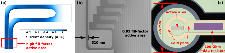
In this work, we introduce the candelabra meander (see supplementary), which utilizes optimized 90-degree and 180-degree bending primitives (defined in the python CAD-layout library phidl McCaughan et al. (2021)) to slowly turn the microwire outside of the active area, enabling us to maintain a high active-area fill factor whilst minimizing current crowding (see fig. 1(a)). The design is inspired by similar structures used in optical waveguides, where a specific length is to be maintained within an area/footprint constraint while minimizing optical loss at the bends. This solution has recently been independently proposed by Jönsson et al. Jönsson et al. (2021). The candelabra meander requires a longer length of microwire to cover the same active area as a traditional meander (see fig. 1(b)), resulting in increased kinetic inductance. Using the silicon-rich tungsten silicide (WSi) recipe developed by Chiles et al. Chiles et al. (2020), we fabricated fiber-coupled, candelabra-meander SMSPDs with 0.51 wide wires and a 0.91 fill factor in the active area. These meanders were embedded in the Bragg-grating and three-layer anti-reflection-coating based optical stack which was previously employed to break the SDE record Reddy et al. (2020). We show that these devices have a near-unity PS of better than 1.02 and a high SDE of better than 91.8% (67% confidence at counts per second) over a wide bandwidth of 40 nm centered at a wavelength of 1550 nm, and SDEs in the range of 96.5-96.9% 0.5% (at counts per second) at 1550 nm. This paves the way for utilization of superconducting microwires for lowering polarization sensitivity in highly-efficient single-photon detectors.
II Fabrication and experimental setup
The SMSPDs presented here were fabricated on a 76.2 mm diameter silicon wafer. Thirteen alternating layers of silicon dioxide (SiO2, thickness nm) and amorphous silicon (Si, thickness nm)–starting with SiO2–were deposited onto the substrate using plasma-enhanced chemical vapor deposition (PECVD), forming a 6.5-period Bragg reflector at 1550 nm. We then deposited gold terminals and 100 palladium-gold (PdAu) speed-up resistors Reddy et al. (2020) (see fig. 1(c)) using a photolithographic lift-off process. We then deposited a 2.2 nm layer of silicon-rich WSi Chiles et al. (2020) with a 2-nm thick Si capping layer using a magnetron sputtering tool. A candelabra meander for wide wires and nm gap width was then patterned onto an electron-beam resist layer.
Due to the ultra-thin nature of the WSi layer (which limits amount of light absorption per transmissive pass), we needed to cover a larger active area than in comparable optical stacks that utilize other materials and thicknesses Reddy et al. (2020) to account for the extra beam divergence. Therefore, the candelabra meander covered a rhomboidal active area with a minor diagonal of length and a major diagonal of length (the shortest possible major diagonal for a given minor diagonal length, fill factor and bend radius). The meander pattern was then transferred onto the WSi layer using SF6-based reactive-ion etching. We then deposited a three-layer anti-reflection (AR) coating of ( nm), SiO2 ( nm), and ( nm) in that order onto the microwire layer. These thicknesses were determined to minimize reflection of vertically incident 1550 nm light using rigorous coupled-wave analysis (RCWA) simulations Moharam and Gaylord (1981); Li et al. (2016). Vias were then selectively etched into the AR-coating to enable wirebonding access to the gold pads. Deep-reactive-ion etching was then used to etch through the wafer substrate in a keyhole pattern (see fig. 1(c)), which enabled easy liberation of the device dies and their mounting into the fiber-ferrule self-aligning package developed by Miller et al. in 2011 Miller et al. (2011). SMF28e+ fiber pigtails terminating at AR-coated, 2.5-mm-diameter ceramic ferrules were then inserted into the self-aligning packages.
Four devices from a single wafer were mounted inside a sorption-based cryostat and cooled to 720-730 mK. The devices were electrically accessible through SMA ports, and optically accessible through splicing into the bare ends of the fiber pigtails outside of the cryostat. The system-detection efficiency (SDE) reported here is defined as the probability for the device to register a detection given that a photon is launched into the fiber pigtail Reddy et al. (2020). All measurements were performed using a highly attenuated, tunable, continuous-wave laser passed through a 1x2 optical switch and two different types of polarization controllers. An all-fiber polarization controller was used for algorithmic polarization optimizations at various wavelengths. A free-space polarization controller was later used to fully scan the Bloch sphere at 1550 nm. A NIST-calibrated power meter, and a rack-mounted, “monitoring” power meter were used for all equipment calibrations Reddy et al. (2020). The devices were quasi-current-biased using a bias tee, a 100 k series resistor, and a programmable voltage source. The detection pulses were amplified using two room-temperature RF amplifiers, conditioned into square pulses using comparators, and plugged into an electronic pulse counter. The design, fabrication, calibration procedures, and error analysis are described in greater detail in the supplementary material.
III Measurement results and discussion
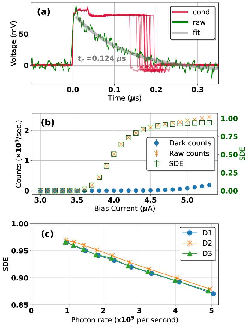
One out of the four mounted devices was found to be electrically open when cooled down. We therefore only present the results for the remaining three devices, labeled D1, D2, and D3. The kinetic inductance of 2.2-nm thick, Si-rich WSi was measured to be , which is nearly thrice the typical value for SNSPDs. This, along with the bigger active area required, counteracts the gains made in decreasing total inductance through micrometer-scale wire widths. We fabricated a 100 speed-up resistor in series with the microwire to gain a factor of two in recovery time Reddy et al. (2020), yielding a value of ns. The width of the comparator-conditioned square pulses averaged to around ns (see fig. 2(a)). The square pulses showed high variance in temporal width due to electronic noise affecting the hysteresis-voltage threshold trigger set at the comparators. Figure 2(b) shows the counts versus current bias for detector D1 at counts per second and 1550 nm photon wavelength. All three detectors showed internal saturation at such count rates, with a dark-count rate of per second when biased at 5 .
Figure 2(c) shows the measured SDE at optimal polarization (optimized using the all-fiber polarization controller and the python nlopt library) versus 1550 nm photon rate for all three devices. The pile-up effect resulting from the ns conditioned-square-pulse reset time Liu et al. (2019); Li et al. (2019), along with any residual device nonlinearity, results in a detection-rate dependent SDE. The standard error bars on the SDE estimate are (0.39-0.42) % at a photon rate of per second, and (0.49-0.52) % at photon rates of per second (see supplementary material). The SDE at photon rates of per second are around 96.5-96.9 % across the three devices, which is comparable to high-efficiency SNSPDs with 100 ns recovery times Reddy et al. (2020). The SDE vs. photon rate trend line indicates that these devices are asymptotically fully efficient at ultra-low photon rates, and that no light is being lost due to beam divergence. We designate a rate of per second as a conservative, dominant regime of application, and report efficiencies and polarization sensitivities at these light levels in the abstract and conclusion of this document. Furthermore, we report all efficiencies at a bias current of , which is about 94-96% of the switching current across all three devices.
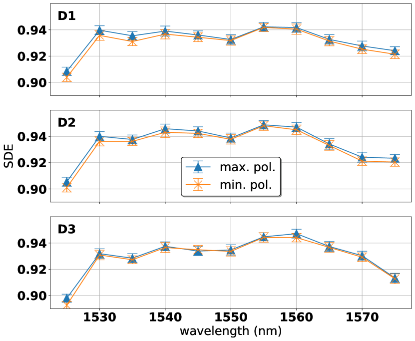
In fig. 3 we plot the SDE for all three devices measured at a photon rate of per second across the wavelength range of 1525-1575 nm. The nlopt python library was used to find the settings for the all-fiber polarization controller that maximized and minimized the SDE at a given incident light level. All three detectors showed mean SDEs greater than 92% in the 1530-1570 nm wavelength range. For reference, the maximum possible SDE (limited due to pile-up effect Coates (1968); Walker (2002)) for devices with a dead-time of 175 ns at a continuous input photon rate of per second is 96.5%. This procedure indicated that the all-fiber-controller-derived PS did not exceed 1.006 across the entire bandwidth measured. The PS in some instances was measured to be very close to unity, resulting in some difficulty in optimization for the nlopt library. The optimization step for device D3 at 1545 nm took nearly half-an-hour to halt for both maximization and minimization, resulting in a “min. pol.” mean-SDE value exceeding the “max. pol.” mean-SDE value.
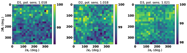
The all-fiber polarization controller is not guaranteed to sample the entire space of polarization states. Therefore we replaced it with a free-space polarization controller, which transmits the light in free-space through a linear polarizer, a quarter-wave plate, and a half-wave plate, all three of which are mounted on controllable rotary mounts in that order. This controller was used to scan the entire Bloch-sphere of polarization states. Figure 4 shows plots for transmission-corrected (see supplementary material) counts normalized to the maximum counts across equally spaced polarization settings on the Bloch sphere for all three detectors. The counts were measured at an average count rate of per second while the detectors were biased at 5 , and the measurement took 20 minutes for each device. Both dark counts and laser power had to be monitored at each polarzation setting. A further 20 minutes was required after each measurement session (per device) to measure the free-space polarization controller transmission correction using two power meters at classical light levels (see supplementary material). This measurement yielded PS of for the three devices without any smoothing function applied to the plotted data. We report a conservative value of for PS for our devices in the abstract and conclusion of this document.
The microwire recipe used in these devices Chiles et al. (2020) required the superconducting layer to be ultra-thin at around 2.2 nm. This is thinner than typical for microwire devices explored thus far Korneeva et al. (2020); Vodolazov et al. (2020); Charaev et al. (2020); Xu et al. (2021). This resulted in a larger active-area requirement, causing a large kinetic inductance. We employed a speed-up resistor to improve the recovery time. This, along with the substantial length of the candelabra meander, resulted in a large timing jitter of 1.5 ns. The candelabra meander, when used in conjunction with superconducting microwires, can trivially hit near-unity PS values Meng et al. (2020b) due to their large fill-factors in the active area. Additionally, the absence of bends within the active area can ensure that the microwires are photon sensitive across their entire lateral width, enabling simultaneous near-unity-PS and high-SDE single-photon detection across a wide range of wavelengths. This capability will prove fruitful for quantum optics experiments involving wavelength-division multiplexing, or time-frequency entanglement spanning the low-loss C-band from fiber-optical communications.
IV Conclusion
We introduced the candelabra meander as a new geometry for superconducting nanowire and microwire single-photon detectors. This meander enables high-fill factors in the active area without the deleterious effects of current crowding at the hairpin bends that plagued the traditional meander geometry. We utilized this in the fabrication of WSi-based SMSPDs with 0.51 wide microwires and a fill factor of 0.91 in the active area. We embedded the SMSPDs in the Bragg-reflector-based optical stack optimized for high efficiency detection of 1550 nm photons. We then fiber-packaged these devices and measured their polarization sensitivities and system-detection efficiencies at various wavelengths and photon rates in the near-IR region. We showed that this design achieves a PS of and high efficiencies of greater than 92% across a 40 nm bandwidth centered at 1550 nm. This furthers the goal of development of fiber-coupled single-photon detectors with joint high performance for multiple measures.
V Data availability statement
All of the experimental data gathered during the measurements made for these results are available on a Zenodo repository: https://doi.org/10.5281/zenodo.6036210. Copies of the same can be provided by the authors upon request. The data and the python code for processing and plotting will be provided as a zip-archive file (SHA-1 91599a67964d30b695b50b4719985533e98869a0) with a digital signature from the primary author (gpg fingerprint: CC49 3CCF 1104 0DC7 36C4 5A7C E4E5 0022 5ED1 7577).
VI Acknowledgments
The authors would like to acknowledge Igor Veyshenker for providing us with power-meter calibration. We thank Dr. Gautam A. Kavuri for help with timing-jitter measurements. We thank Prof. Juliet Gopinath and her group for accommodating our cryostat and experimental setup in their laboratory space in the EECE department at University of Colorado, Boulder.
References
- Hochberg et al. (2019) Y. Hochberg, I. Charaev, S. W. Nam, V. Verma, M. Colangelo, and K. K. Berggren, Physical Review Letters 123, 151802 (2019).
- Mao et al. (2018) Y. Mao, B.-X. Wang, C. Zhao, G. Wang, R. Wang, H. Wang, F. Zhou, J. Nie, Q. Chen, Y. Zhao, and et al., Optics Express 26, 6010 (2018).
- Chen et al. (2020) J.-P. Chen, C. Zhang, Y. Liu, C. Jiang, W. Zhang, X.-L. Hu, J.-Y. Guan, Z.-W. Yu, H. Xu, J. Lin, and et al., Physical Review Letters 124, 070501 (2020).
- Slussarenko et al. (2017) S. Slussarenko, M. M. Weston, H. M. Chrzanowski, L. K. Shalm, V. B. Verma, S. W. Nam, and G. J. Pryde, Nature Photonics 11, 700–703 (2017).
- Zhu et al. (2017) J. Zhu, Y. Chen, L. Zhang, X. Jia, Z. Feng, G. Wu, X. Yan, J. Zhai, Y. Wu, Q. Chen, and et al., Scientific Reports 7, 15113 (2017).
- Chen et al. (2018) L. Chen, D. Schwarzer, J. A. Lau, V. B. Verma, M. J. Stevens, F. Marsili, R. P. Mirin, S. W. Nam, and A. M. Wodtke, Optics Express 26, 14859 (2018).
- Zhuang, Zhang, and Shapiro (2018) Q. Zhuang, Z. Zhang, and J. H. Shapiro, Physical Review A 97, 032329 (2018).
- Khabiboulline et al. (2019) E. Khabiboulline, J. Borregaard, K. De Greve, and M. Lukin, Physical Review Letters 123, 070504 (2019).
- Shibata, Honjo, and Shimizu (2014) H. Shibata, T. Honjo, and K. Shimizu, Optics Letters 39, 5078 (2014).
- Dixon et al. (2014) P. B. Dixon, D. Rosenberg, V. Stelmakh, M. E. Grein, R. S. Bennink, E. A. Dauler, A. J. Kerman, R. J. Molnar, and F. N. C. Wong, Physical Review A 90, 043804 (2014).
- Shalm et al. (2015) L. K. Shalm, E. Meyer-Scott, B. G. Christensen, P. Bierhorst, M. A. Wayne, M. J. Stevens, T. Gerrits, S. Glancy, D. R. Hamel, M. S. Allman, and et al., Physical Review Letters 115, 250402 (2015).
- Takesue et al. (2015) H. Takesue, S. D. Dyer, M. J. Stevens, V. Verma, R. P. Mirin, and S. W. Nam, Optica 2, 832 (2015).
- Najafi et al. (2015) F. Najafi, J. Mower, N. C. Harris, F. Bellei, A. Dane, C. Lee, X. Hu, P. Kharel, F. Marsili, S. Assefa, and et al., Nature Communications 6, 5873 (2015).
- Jin et al. (2015) J. Jin, E. Saglamyurek, M. G. Puigibert, V. Verma, F. Marsili, S. W. Nam, D. Oblak, and W. Tittel, Physical Review Letters 115, 140501 (2015).
- Weston et al. (2016) M. M. Weston, H. M. Chrzanowski, S. Wollmann, A. Boston, J. Ho, L. K. Shalm, V. B. Verma, M. S. Allman, S. W. Nam, R. B. Patel, and et al., Optics Express 24, 10869 (2016).
- Saglamyurek et al. (2016) E. Saglamyurek, M. G. Puigibert, Q. Zhou, L. Giner, F. Marsili, V. B. Verma, S. Woo Nam, L. Oesterling, D. Nippa, D. Oblak, and et al., Nature Communications 7, 11202 (2016).
- Reddy et al. (2020) D. V. Reddy, R. R. Nerem, S. W. Nam, R. P. Mirin, and V. B. Verma, Optica 7, 1649 (2020).
- Hu et al. (2020) P. Hu, H. Li, L. You, H. Wang, Y. Xiao, J. Huang, X. Yang, W. Zhang, Z. Wang, and X. Xie, Optics Express 28, 36884 (2020).
- Chang et al. (2021) J. Chang, J. W. N. Los, J. O. Tenorio-Pearl, N. Noordzij, R. Gourgues, A. Guardiani, J. R. Zichi, S. F. Pereira, H. P. Urbach, V. Zwiller, and et al., APL Photonics 6, 036114 (2021).
- Korzh et al. (2020) B. Korzh, Q.-Y. Zhao, J. P. Allmaras, S. Frasca, T. M. Autry, E. A. Bersin, A. D. Beyer, R. M. Briggs, B. Bumble, M. Colangelo, and et al., Nature Photonics 14, 250–255 (2020).
- Shibata et al. (2017) H. Shibata, K. Fukao, N. Kirigane, S. Karimoto, and H. Yamamoto, IEEE Transactions on Applied Superconductivity 27, 1–4 (2017).
- Anant et al. (2008) V. Anant, A. J. Kerman, E. A. Dauler, J. K. W. Yang, K. M. Rosfjord, and K. K. Berggren, Optics Express 16, 10750 (2008).
- Redaelli et al. (2016) L. Redaelli, G. Bulgarini, S. Dobrovolskiy, S. N. Dorenbos, V. Zwiller, E. Monroy, and J. M. Gérard, Superconductor Science and Technology 29, 065016 (2016).
- Zheng et al. (2016) F. Zheng, R. Xu, G. Zhu, B. Jin, L. Kang, W. Xu, J. Chen, and P. Wu, Scientific Reports 6 (2016), 10.1038/srep22710.
- Redaelli et al. (2017) L. Redaelli, V. Zwiller, E. Monroy, and J. M. Gérard, Superconductor Science and Technology 30, 035005 (2017).
- Reddy et al. (2019) D. V. Reddy, R. R. Nerem, A. E. Lita, S. W. Nam, R. P. Mirin, and V. B. Verma, Conference on Lasers and Electro-Optics (2019), 10.1364/cleo_qels.2019.ff1a.3.
- Ghafari et al. (2019) F. Ghafari, N. Tischler, J. Thompson, M. Gu, L. K. Shalm, V. B. Verma, S. W. Nam, R. B. Patel, H. M. Wiseman, and G. J. Pryde, Physical Review X 9 (2019), 10.1103/physrevx.9.041013.
- Shalm et al. (2021) L. K. Shalm, Y. Zhang, J. C. Bienfang, C. Schlager, M. J. Stevens, M. D. Mazurek, C. Abellán, W. Amaya, M. W. Mitchell, M. A. Alhejji, and et al., Nature Physics 17, 452–456 (2021).
- Wei et al. (2019) K. Wei, W. Zhang, Y.-L. Tang, L. You, and F. Xu, Physical Review A 100 (2019), 10.1103/physreva.100.022325.
- Dorenbos et al. (2008) S. N. Dorenbos, E. M. Reiger, N. Akopian, U. Perinetti, V. Zwiller, T. Zijlstra, and T. M. Klapwijk, Applied Physics Letters 93, 161102 (2008).
- Henrich et al. (2013) D. Henrich, L. Rehm, S. Dorner, M. Hofherr, K. Il’in, A. Semenov, and M. Siegel, IEEE Transactions on Applied Superconductivity 23, 2200405–2200405 (2013).
- Huang et al. (2017) J. Huang, W. J. Zhang, L. X. You, X. Y. Liu, Q. Guo, Y. Wang, L. Zhang, X. Y. Yang, H. Li, Z. Wang, and et al., Superconductor Science and Technology 30, 074004 (2017).
- Verma et al. (2012) V. B. Verma, F. Marsili, S. Harrington, A. E. Lita, R. P. Mirin, and S. W. Nam, Applied Physics Letters 101, 251114 (2012).
- Gu et al. (2015) C. Gu, Y. Cheng, X. Zhu, and X. Hu, Advanced Photonics 2015 (2015), 10.1364/iprsn.2015.jm3a.10.
- Chi et al. (2018) X. Chi, K. Zou, C. Gu, J. Zichi, Y. Cheng, N. Hu, X. Lan, S. Chen, Z. Lin, V. Zwiller, and et al., Optics Letters 43, 5017 (2018).
- Meng et al. (2020a) Y. Meng, K. Zou, N. Hu, X. Lan, L. Xu, J. Zichi, S. Steinhauer, V. Zwiller, and X. Hu, Optics Letters 45, 471 (2020a).
- Meng et al. (2020b) Y. Meng, K. Zou, N. Hu, L. Xu, X. Lan, S. Steinhauer, S. Gyger, V. Zwiller, and X. Hu, “Fractal superconducting nanowires detect infrared single photons with 91% polarization-independent system efficiency and 19 ps timing resolution,” (2020b), arXiv:2012.06730, arxiv:arXiv:2012.06730 .
- Clem and Berggren (2011) J. R. Clem and K. K. Berggren, Physical Review B 84 (2011), 10.1103/physrevb.84.174510.
- Xu et al. (2017) R. Xu, F. Zheng, D. Qin, X. Yan, G. Zhu, L. Kang, L. Zhang, X. Jia, X. Tu, B. Jin, and et al., Journal of Lightwave Technology 35, 4707–4713 (2017).
- Mukhtarova et al. (2018) A. Mukhtarova, L. Redaelli, D. Hazra, H. Machhadani, S. Lequien, M. Hofheinz, J.-L. Thomassin, F. Gustavo, J. Zichi, V. Zwiller, and et al., Optics Express 26, 17697 (2018).
- Xu et al. (2018) R. Xu, Y. Li, F. Zheng, G. Zhu, L. Kang, L. Zhang, X. Jia, X. Tu, Q. Zhao, B. Jin, and et al., Optics Express 26, 3947 (2018).
- Li and Jiao (2019) D. Li and R. Jiao, Photonics Research 7, 847 (2019).
- McCaughan et al. (2021) A. N. McCaughan, A. N. Tait, S. M. Buckley, D. M. Oh, J. T. Chiles, J. M. Shainline, and S. W. Nam, Journal of Vacuum Science & Technology B 39, 062601 (2021).
- Yang et al. (2021) C. Yang, M. Si, X. ZHANG, A. Yu, h. jia, Y. Pan, H. Li, L. Li, Z. Wang, S. Zhang, and et al., Optics Express (2021), 10.1364/oe.422581.
- Korneeva et al. (2020) Y. P. Korneeva, N. Manova, I. Florya, M. Y. Mikhailov, O. Dobrovolskiy, A. Korneev, and D. Y. Vodolazov, Physical Review Applied 13 (2020), 10.1103/physrevapplied.13.024011.
- Chiles et al. (2020) J. Chiles, S. M. Buckley, A. Lita, V. B. Verma, J. Allmaras, B. Korzh, M. D. Shaw, J. M. Shainline, R. P. Mirin, and S. W. Nam, Applied Physics Letters 116, 242602 (2020).
- Vodolazov et al. (2020) D. Vodolazov, N. Manova, Y. Korneeva, and A. Korneev, Physical Review Applied 14 (2020), 10.1103/physrevapplied.14.044041.
- Charaev et al. (2020) I. Charaev, Y. Morimoto, A. Dane, A. Agarwal, M. Colangelo, and K. K. Berggren, Applied Physics Letters 116, 242603 (2020).
- Lita et al. (2021) A. E. Lita, V. B. Verma, J. Chiles, R. P. Mirin, and S. W. Nam, Superconductor Science and Technology 34, 054001 (2021).
- Steinhauer, Gyger, and Zwiller (2021) S. Steinhauer, S. Gyger, and V. Zwiller, Applied Physics Letters 118, 100501 (2021).
- Xu et al. (2021) G.-Z. Xu, W.-J. Zhang, L.-X. You, J.-M. Xiong, X.-Q. Sun, H. Huang, X. Ou, Y.-M. Pan, C.-L. Lv, H. Li, and et al., Photonics Research 9, 958 (2021).
- Yang et al. (2009) J. Yang, A. Kerman, E. Dauler, B. Cord, V. Anant, R. Molnar, and K. Berggren, IEEE Transactions on Applied Superconductivity 19, 318–322 (2009).
- Baghdadi et al. (2021) R. Baghdadi, E. Schmidt, S. Jahani, I. Charaev, M. G. W. Müller, M. Colangelo, D. Zhu, K. Ilin, A. D. Semenov, Z. Jacob, and et al., Superconductor Science and Technology 34, 035010 (2021).
- Xiong et al. (2021) J.-M. Xiong, W.-J. Zhang, G.-Z. Xu, L.-X. You, X.-Y. Zhang, L. Zhang, C.-J. Zhang, D.-H. Fan, Y.-Z. Wang, H. Li, and Z. Wang, “Reducing current crowding in meander superconducting strip single-photon detectors by thickening bends,” (2021), arXiv:2112.08009, arxiv:arXiv:2112.08009 .
- Jönsson et al. (2021) M. Jönsson, R. Vedin, S. Gyger, J. A. Sutton, S. Steinhauer, V. Zwiller, M. Wallin, and J. Lidmar, “Current crowding in nanoscale superconductors within the ginzburg-landau model,” (2021), arXiv:2112.05443, arxiv:arXiv:2112.05443 .
- Moharam and Gaylord (1981) M. G. Moharam and T. K. Gaylord, Journal of the Optical Society of America 71, 811 (1981).
- Li et al. (2016) H. Li, S. Chen, L. You, W. Meng, Z. Wu, Z. Zhang, K. Tang, L. Zhang, W. Zhang, X. Yang, and et al., Optics Express 24, 3535 (2016).
- Miller et al. (2011) A. J. Miller, A. E. Lita, B. Calkins, I. Vayshenker, S. M. Gruber, and S. W. Nam, Optics Express 19, 9102 (2011).
- Liu et al. (2019) S. Liu, X.-R. Yao, X.-F. Liu, D.-Z. Xu, X.-D. Wang, B. Liu, C. Wang, G.-J. Zhai, and Q. Zhao, Optics Express 27, 22138 (2019).
- Li et al. (2019) B. Li, G. Deng, R. Zhang, Z. Ou, H. Zhou, Y. Ling, Y. Wang, Y. Wang, K. Qiu, H. Song, and Q. Zhou, J. Lightwave Technol. 37, 5899 (2019).
- Coates (1968) P. B. Coates, Journal of Physics E: Scientific Instruments 1, 878–879 (1968).
- Walker (2002) J. G. Walker, Optics Communications 201, 271–277 (2002).