Clean quantum point contacts in an InAs quantum well grown on a lattice-mismatched InP substrate
Abstract
Strong spin-orbit coupling, the resulting large factor, and small effective mass make InAs an attractive material platform for inducing topological superconductivity. The surface Fermi level pinning in the conduction band enables highly transparent ohmic contact without excessive doping. We investigate electrostatically-defined quantum point contacts (QPCs) in a deep-well InAs two-dimensional electron gas. Despite the 3.3% lattice mismatch between the InAs quantum well and the InP substrate, we report clean QPCs with up to eight pronounced quantized conductance plateaus at zero magnetic field. Source-drain dc bias spectroscopy reveals a harmonic confinement potential with a nearly meV subband spacing. We find a many-body exchange interaction enhancement for the out-of-plane factor , whereas the in-plane factor is isotropic , close to the bulk value for InAs.
I Introduction
A quantum point contact (QPC) is a ballistic quasi one-dimensional constriction with a tunable conductance, quantized in multiples of [1]. First demonstrated in GaAs/AlxGa1-xAs two-dimensional electron gases (2DEGs) over three decades ago [2, 3], QPCs have been incorporated into mesoscale quantum devices for tunnel spectroscopy [4], quantum dots [5], charge sensors [6, 7], electron injectors [8], spin polarizers [9], electronic beam splitters [10], and more. However, demonstrations of clean QPCs in InAs heterostructures remain far fewer.
InAs-based nanostructures have come under a renewed spotlight as a potential platform for proximity-induced topological superconductivity [11, 12]. InAs has a small effective mass, large spin-orbit coupling, and surface Fermi level pinning [13]. Proximitized by an -wave superconductor and exposed to a magnetic field, a one-dimensional InAs nanostructure should host Majorana zero modes at its ends [14, 15, 16]. This makes InAs-based systems an enticing platform for observing and manipulating Majorana zero modes, toward possible eventual topological quantum information processing [17, 18, 19, 20]. InAs 2DEGs can be top-down patterned, offering a scaling advantage over directly-grown nanowires for creating complex geometries and for scaling to large numbers of devices [12, 21]. The small effective mass [22, 23] in InAs quantum wells (QWs) results in a weak temperature and bias dependence of resistivity, making it easier to decouple the background 2DEG in transport measurements of the QPC. Furthermore, a single valley degree of freedom with large bulk factor 12-15 makes InAs QWs a promising material platform for fast control of spin qubits [28, 29, 30] and quantum simulation of many-body phases [31, 32]. Clean QPCs with smoothly tunable transitions are a key building block for integrating InAs quantum dot arrays in quantum simulators and processors.
We report the investigation of quantized conductance and magnetotransport properties of a narrow gate-defined constriction, fabricated in a buried InAs 2DEG grown by molecular beam epitaxy (MBE) on an InP substrate. The 3.3% lattice mismatch [13] between InAs and InP leads to a compressive strain on the quantum well and introduces dislocation defects; we demonstrate that despite this, our QPCs are the cleanest amongst the handful of reported works in etched and gate-defined constrictions in InAs and InAs/InGaAs QWs [Debray2009, 33, 34, 35, 36]. The more closely lattice-matched substrate choice of GaSb has been plagued for decades with trivial edge conduction at mesa edges [37, 38, 39, 40] which complicates interpretation of transport measurements. Though purely gate-defined nanostructures have recently allowed circumventing this [41, 35], InP has superior insulating properties compared to GaSb, simplifying the fabrication and operation of quantum devices. The QPC featured in this paper shows eight pronounced quantized conductance plateaus with a harmonic subband spacing near meV. The spin-split conductance plateaus in an applied magnetic field let us extract an isotropic in-plane effective factor and an exchange interaction-enhanced out-of-plane . Our work supports the integration of QPCs into quantum dots and other nanostructures.
II Device fabrication and experiment setup
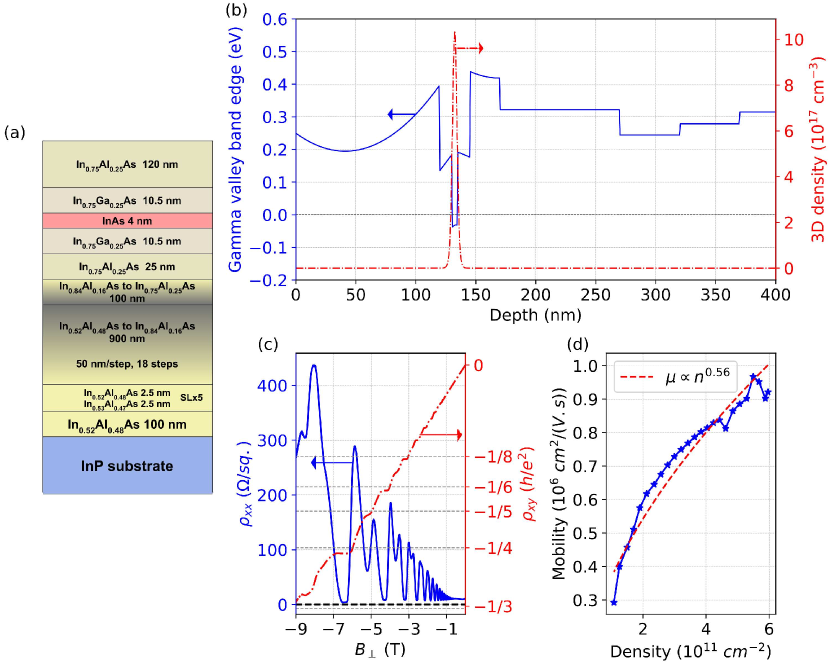
The device was fabricated on a heterostructure grown by MBE on a semi-insulating InP (100) substrate; the growth is characterized in detail in Ref. 42 (Sample B). The layer sequence is shown in the cross-sectional schematic Fig. S1(a) in the Supplemental Material (SM) [23]. The active region consists of a 4 nm InAs QW sandwiched between 10.5 nm of In0.75Ga0.25As layers. A 900 nm step-graded buffer of InxAl1-xAs helps overcome the native lattice mismatch between InP and the quantum well, and a 120 nm In0.75Al0.25As top barrier moves the active region away from the surface for increased mobility.
Carriers originating from deep-level donor states in the In0.75Al0.25As layers populate the 2DEG formed in the InAs QW [43, 44]. The 2DEG has a mobility cm2/Vs at an electron density cm-2 as measured in a 5 m-wide Hall bar at K, corresponding to a mean-free path of m. Owing to suppressed alloy and InGaAs/InAs interface scattering in our buried deep-well heterostructure, the mobility is amongst the highest reported for InAs QWs and is limited by unintentional background impurities and native charged point defects [23, 42].
Our samples are first processed with standard electron beam lithography and wet etching to define an extended Hall bar-like mesa with an area of 5 m 60 m between voltage probes. The etch depth is 300 nm, extending into the buffer layer to achieve electrical isolation. To improve surface and edge contact, Ti/Au ohmic contacts are deposited after a light, additional wet etch and in situ Ar mill. A 35-nm HfO2 dielectric layer is added by atomic layer deposition at 150 °C. Finally, Ti/Au gate electrodes are deposited in multiple steps to form pairs of split gates of width 100 nm () and lithographically designed separations in the range 175 – 475 nm. The QPC highlighted in this work has separation 325 nm, and data from additional QPCs are included in the SM [23].
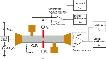
The measurements reported here are performed at K in a pumped He-4 cryostat, over multiple cooldowns. A low frequency (20 Hz) ac excitation of 100 V rms is applied between the source (S) and drain (D) contacts on the extended Hall bar. The current at the drain, , and diagonal voltage drop across the QPC, , are measured using standard low-frequency lock-in techniques. A schematic of the measurement configuration is shown in Fig. 1. The conductance through the QPC is , where is the gate-independent 2DEG resistance between the voltage probes.
III Results and Discussion
III.1 Conductance quantization
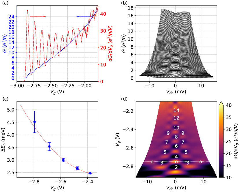
Negatively biasing the split gates with a voltage around V depletes the 2DEG directly underneath, forming a quasi-one-dimensional constriction. Upon further biasing, Fig. 2(a) clearly shows eight plateaus in at even multiples of the conductance quantum as a function of symmetric gate voltage (), signifying ballistic transport through the spin-degenerate one-dimensional subbands in the gate-defined constriction, before completely pinching off around V. Beyond pinch-off, the current is below the noise-floor of the preamplifier pA, implying a pinch-off resistance . The appearance of eight quantized conductance plateaus reveals the pristine nature of the constriction defined by the QPC, and exceeds previous reports [35, 36]. This is compatible with the lithographic split-gate separation nm and Fermi wavelength nm in the 2DEG. The constriction is well described by a saddle-point model in the few-mode limit (, as shown in the SM [23] and the references [24, 25] therein. Immediately after cooling the sample, we often observe that pinch-off and other conductance features in vs gradually drift toward more negative gate voltages. This could be due to the dynamics of charge traps within the dielectric layer. After a few days, conductance features in repeated voltage sweeps become reproducible to within a 1 mV relative voltage shift. For consistency, we report data measured with swept upwards, although once the potential drift stabilizes no significant difference is observed between the two sweep directions.
III.2 Finite-bias spectroscopy
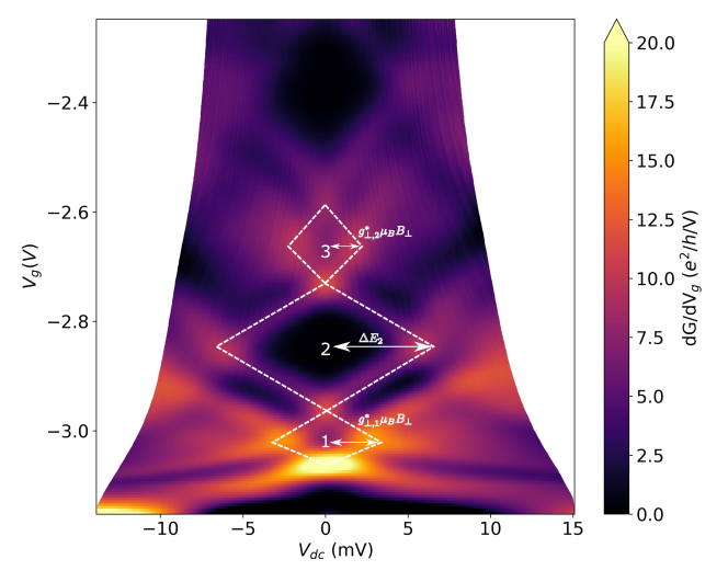
The level spectrum of the constriction can be probed by applying a dc bias voltage across the source and drain electrodes of the device. The dc voltage drop across the QPC, , is obtained by subtracting the voltage drop across the bare 2DEG: , where is the four-terminal dc voltage difference measured across the QPC, is the dc current through the Hall bar, and is a series resistance arising from the mesa 2DEG resistance. Figure 2(b) plots as a function of , where each trace corresponds to a particular , as the QPC is opened from pinch-off. A bunching of traces is observed at conductance plateaus, which are even multiples of at low-bias, and odd multiples at high-bias. The transconductance is shown in Fig. 2(d) as a function of and , with the dark regions corresponding to conductance plateaus and bright regions representing transitions.
The extent of the transconductance diamond for along is a common measure [45] of the energy spacing of QPC subbands at the gate voltage corresponding to the diamond endpoints. Opening the QPC from pinch-off decreases the curvature of the confinement potential, decreasing the subband spacing with as shown in Fig. 2(c). The harmonicity of the confinement potential in a particular gate voltage range can be probed by considering a triplet of transconductance maxima circled in Fig. 2(d). Since they occur at approximately the same gate voltage, we infer [45]. Similar horizontal lines can be drawn connecting diamond vertices at higher conductances, implying a harmonic confinement potential, albeit a function of .
Approximating the lateral confinement as a harmonic potential with a gate voltage-dependent angular frequency , the length scale of the transverse real-space extent of the subbands at = ∗ can be estimated as
| (1) |
where [22, 23] is the effective mass and is the bare electron mass. Taking for the subband spacing as determined above, the corresponding length scales can be estimated as nm, nm and nm for the first three subbands, consistent with expectations from the lithographic width = 325 nm .
III.3 In-plane magnetic field
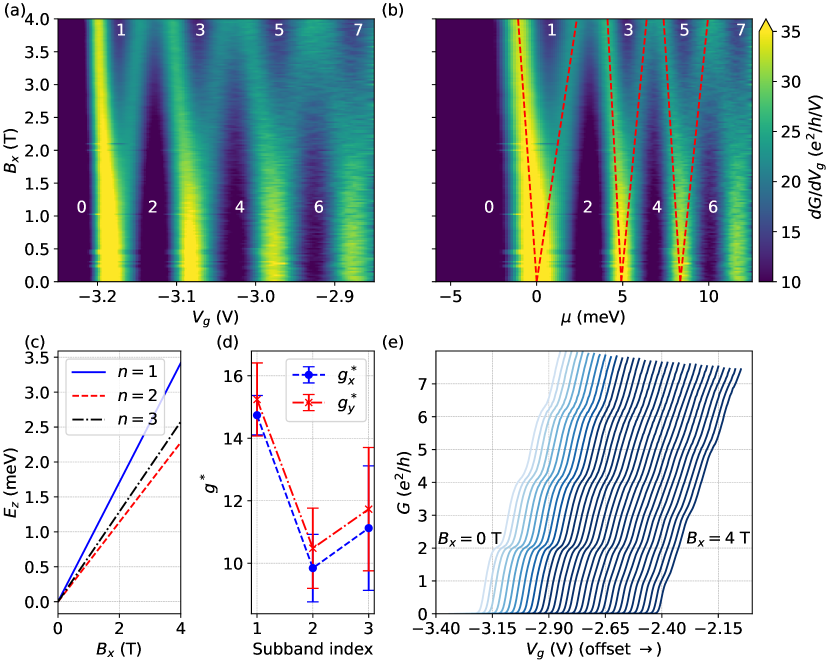
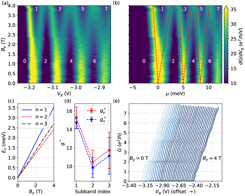
Spin-resolved transport through the QPC can be studied by applying a magnetic field in the plane of the sample and parallel to the transport direction. Figure 3(a) shows the transconductance as a function of and , as the gate voltage is swept up from pinch-off. The dark, diamond-shaped regions at low correspond to the spin-degenerate even-integer conductance plateaus. At higher applied , the spin splitting by the Zeeman effect dominates over the subband linewidths, resulting in the appearance of odd plateaus as additional dark regions interleaved with the spin-degenerate diamonds. Conductance traces as a function of for different are shown in Fig. 3(e). As expected, conductance plateaus at and emerge as is increased and the width of the even-integer plateaus correspondingly decreases.
Figure 3(b) elucidates the spin-split subband spectrum by translating to a chemical potential , using the split-gate lever arm extracted from Fig. 2(d) (see the SM [23] for details on the conversion). A linear fit to the transconductance maxima for each spin-split subband pair is used to extract the Zeeman energy as a function of , as depicted in Fig. 3(c). These linear fits were constrained to intersect at for each spin-split subband pair. The in-plane factor extracted from the slope of the Zeeman energy is shown in Fig. 3(d), with error estimates based on fitting parameter variances. Figure 3(d) also shows the in-plane factor measured in a magnetic field in-plane but perpendicular to the direction of transport, revealing negligible anisotropy (see the SM [23]). This is consistent with previous measurements in (In,Ga)As [46], InSb [47] and n-type GaAs [48] QPCs. The isotropic in-plane factor points to a weak Rashba spin-orbit coupling in the constriction [49]. The absence of intentional dopants and the symmetric In0.75Ga0.25As barrier structure in the QW stack result in a symmetric 2DEG confinement potential. As revealed by self-consistent Schrödinger-Poisson simulations, the QW hosts an electron wavefunction with symmetric tails in the barrier regions [see Fig. S1(b)] in the SM [23]). This inversion symmetry of QW in the growth direction [001] leads to the isotropic effective factor for in-plane magnetic fields [50]. Furthermore, the estimated in-plane factor for the first three subbands is typical for bulk InAs ( [51, 52]), with an enhancement for the subband in agreement with theoretical predictions based on exchange interactions [53, 54].
III.4 Out-of-plane magnetic field
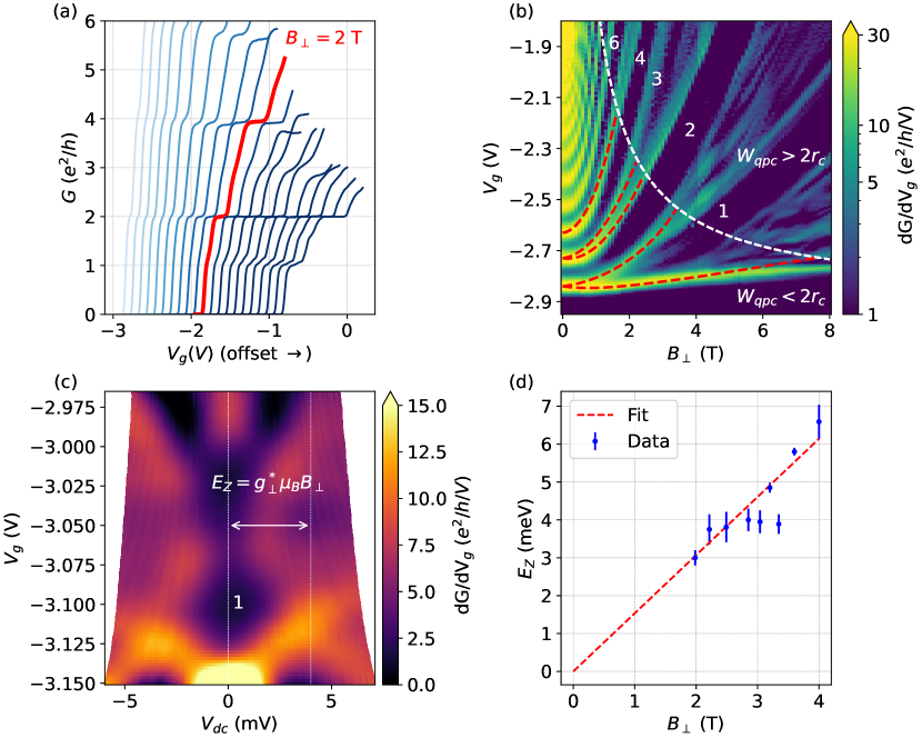
As a next step in investigating the QPC, we study the effect of electrostatic confinement on magnetic subbands by applying a magnetic field perpendicular to the plane of the sample. The conductance as is swept up from pinch-off for is shown in Fig. 4(a). The cyclotron energy of the electrons, where is the electron charge, adds in quadrature to the QPC confinement energy. The resultant magnetoelectric subbands have a spacing that initially grows quadratically with field before transitioning into a linear increase as they line up with the 2DEG Landau levels for [56], where is the cyclotron radius of the classical electron trajectory in the 2DEG, is the Fermi wave number in the 2DEG, and is the gate voltage-dependent constriction width (see Sec. S6 in the SM [23]). The increase in subband spacing and suppression of backscattering through the Hall bar with results in broader and more pronounced conductance plateaus. Furthermore, the Zeeman effect of the applied field lifts spin degeneracy and results in the emergence of odd-integer conductance plateaus. Because of thermal ( ) and disorder broadening in our measurements, we observe spin-split plateaus only at T (red trace).
Figure 4(b) depicts the transconductance as a function of and . The dark regions correspond to conductance plateaus, separated by bright features which represent the transitions between the plateaus. The transconductance has a local maximum whenever a subband edge is resonant with the source and/or drain chemical potential. Given that the confinement is described by a -dependent harmonic potential, the magnetoelectric subbands can be described by the Beenakker and van Houten model [55]
| (2) |
where is the spin-degenerate subband index, labels the spin-split subband with spin oriented antiparallel (parallel) to , is the energy offset of the conduction band edge, is the -dependent QPC subband spacing at (see Fig. 2(d)), and is the effective out-of-plane factor. The white dashed curve in Fig. 4(b) marks the contour . An agreement to Eq. 2, when translated to gate voltage, in the low-field regime for is shown as red dotted lines in Fig. 4(b). The spin-degenerate part of Eq. 2 is used for the subband edge since spin splitting is not well observed for .
The Zeeman energy can be measured by performing finite-bias spectroscopy of the QPC as a function of . In a setup identical to Sec. III.2, the QPC conductance is measured as a function of an applied dc voltage at a fixed . Figure 4(c) shows the transconductance as a function of the dc voltage drop across the QPC and around the plateau at T. The dark highlighted region corresponds to the plateau, the extent of which along corresponds to the Zeeman energy meV. Measured as a function of , Fig. 4(d) shows the Zeeman energy evolution with field which fits a straight line constrained to pass through the origin, for . The uncertainty in ascertaining the boundaries of the plateau, as evinced by broadened transconductance peaks in Fig. 4(c), results in large error bars for the Zeeman energies, defined as the width corresponding to 99% relative peak height. This can also be seen from the broad transconductance peaks in the T region of Fig. 4(b). Nevertheless, we can report a two-fold enhancement of the out-of-plane factor compared to the in-plane and bulk InAs value .
The reduced symmetry in quasi-2D heterostructures, as compared to the bulk, introduces anisotropy between and [50]. Furthermore, as previously measured [46] and analyzed [49] for (In,Ga)As QPCs, the orbital effect of the out-of-plane field strengthens many-body exchange interactions in the 2DEG, resulting in an enhanced . The depopulation of consecutive spin-split Landau levels with leads to an oscillatory exchange enhancement, with local maxima at odd filling factors [57, 58, 59]. Sadofyev et al. [58] measured an enhanced out-of-plane factor at high fields in InAs/AlSb QWs. Similar measurements for in our QW reveal an enhanced 2DEG factor in the T field range (see the SM [23]). Consequently, we attribute the enhanced splitting of the QPC subband [Fig. 4(c) and 4(d)] to many-body exchange interactions in the 2DEG, rather than 1D confinement effects due to the constriction.
III.5 Shifting the confinement potential
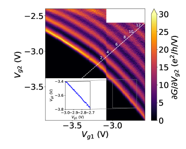
By applying an asymmetric voltage bias to the QPC split gates, we can laterally shift the position of the confining potential in real space. This serves as a spatial map of localized disorder or other potential fluctuations which may increase backscattering in the channel or create accidental quantum dots [60]. Tuning the two gate voltages independently, the transconductance with respect to the fast sweep axis is shown in Fig. 5. The bright features correspond to transitions between conductance plateaus, and they appear consistently smooth across the entire range. Resonances caused by localized disorder would appear as additional gate voltage-dependent lines in this map; the absence of such features here suggests a clean, defect-free channel within this range. Tuning the gate asymmetry to avoid spurious resonances is a common technique in QPC operation—not needing it here will significantly simplify the operation of devices with larger numbers of gates, where cross-capacitances must be diligently accounted for. The blue dots in the inset show a fit to the first transconductance peak in the V and V range. The discontinuities in the fit are due to a drift in the QPC conductance between traces along the slow sweep axis . We additionally note that we do not observe signatures of the 0.7 anomaly or of half-quantized plateaus at zero magnetic field in this QPC, though they have been reported previously in similar structures [33, 36, 34]. This raises the question of the universality of such features in heterostructures of this type.
IV Conclusion
We have presented the fabrication and characterization of a QPC in an InAs-based deep quantum well which displays remarkable cleanliness despite the lattice-mismatched InP substrate. Transport through the QPC is smoothly quantized at zero and finite B-field, and bias spectroscopy reveals a harmonic confining potential with large subband spacing of near meV. We find an isotropic in-plane factor and an out-of-plane factor .
This study supports the integration of QPCs as tunable tunnel barriers, charge sensors [6, 7], or mode collimators [8, 10] into more complex InAs-based two-dimensional quantum devices such as quantum dots. This is a critical building block toward investigations in spintronics, spin qubits, and hybrid superconductor-semiconductor topological physics.
The data that support the findings of this study are available from the corresponding author upon request.
Acknowledgements.
We thank W. Pouse, E. Mikheev, J. Williams, M. Pendharkar, A.C.C. Drachmann, K. Ensslin, T. Ihn, Z. Lei, H. Sahasrabudhe, R. Rahman and F. Pierre for their scientific insights and suggestions. Measurement and analysis were supported by the U.S. Department of Energy (DOE), Office of Science, Basic Energy Sciences (BES), under Contract No. DE-AC02-76SF00515. Growth and characterization of heterostructures was supported by Microsoft Quantum. C.L.H. acknowledges support from the National Science Foundation (NSF) and Stanford Graduate Fellowship (SGF). Part of this work was performed at the Stanford Nano Shared Facilities (SNSF), supported by the National Science Foundation under Award No. ECCS-2026822.References
- van Houten and Beenakker [1996] H. van Houten and C. Beenakker, Phys. Today 49(7), 22 (1996).
- van Wees et al. [1988] B. J. van Wees, H. van Houten, C. W. J. Beenakker, J. G. Williamson, L. P. Kouwenhoven, D. van der Marel, and C. T. Foxon, Phys. Rev. Lett. 60, 848 (1988).
- Wharam et al. [1988] D. A. Wharam, T. J. Thornton, R. Newbury, M. Pepper, H. Ahmed, J. E. F. Frost, D. G. Hasko, D. C. Peacock, D. A. Ritchie, and G. A. C. Jones, J. Phys. C 21, L209 (1988).
- Kjaergaard et al. [2016] M. Kjaergaard, F. Nichele, H. J. Suominen, M. P. Nowak, M. Wimmer, A. R. Akhmerov, J. A. Folk, K. Flensberg, J. Shabani, C. J. Palmstrøm, et al., Nat. Commun. 7 (2016).
- Meirav, Kastner, and Wind [1990] U. Meirav, M. Kastner, and S. Wind, Phys. Rev. Lett. 65, 771 (1990).
- Elzerman et al. [2004] J. M. Elzerman, R. Hanson, L. H. Willems van Beveren, B. Witkamp, L. M. K. Vandersypen, and L. P. Kouwenhoven, Nature (London) 430, 431 (2004).
- Reilly et al. [2007] D. Reilly, C. Marcus, M. Hanson, and A. Gossard, Appl. Phys. Lett. 91, 162101 (2007).
- Van Houten et al. [1988] H. Van Houten, B. Van Wees, J. Mooij, C. Beenakker, J. Williamson, and C. Foxon, Europhys. Lett. 5, 721 (1988).
- Debray et al. [2009a] P. Debray, S. M. S. Rahman, J. Wan, R. S. Newrock, M. Cahay, A. T. Ngo, S. E. Ulloa, S. T. Herbert, M. Muhammad, and M. Johnson, Nat. Nanotechnol. 4, 759 (2009a).
- Ji et al. [2003] Y. Ji, Y. Chung, D. Sprinzak, M. Heiblum, D. Mahalu, and H. Shtrikman, Nature (London) 422, 415 (2003).
- Deng et al. [2016] M. T. Deng, S. Vaitiekenas, E. B. Hansen, J. Danon, M. Leijnse, K. Flensberg, J. Nygård, P. Krogstrup, and C. M. Marcus, Science 354, 1557 (2016).
- Fornieri et al. [2019] A. Fornieri, A. M. Whiticar, F. Setiawan, E. Portolés, A. C. C. Drachmann, A. Keselman, S. Gronin, C. Thomas, T. Wang, R. Kallaher, G. C. Gardner, E. Berg, M. J. Manfra, A. Stern, C. M. Marcus, and F. Nichele, Nature (London) 569, 89 (2019).
- Vurgaftman, Meyer, and Ram-Mohan [2001] I. Vurgaftman, J. R. Meyer, and L. R. Ram-Mohan, J. Appl. Phys. 89, 5815 (2001).
- Oreg, Refael, and Von Oppen [2010] Y. Oreg, G. Refael, and F. Von Oppen, Physical review letters 105, 177002 (2010).
- Lutchyn, Sau, and Sarma [2010] R. M. Lutchyn, J. D. Sau, and S. D. Sarma, Phys. Rev. Lett. 105, 077001 (2010).
- Lutchyn et al. [2018] R. M. Lutchyn, E. P. A. M. Bakkers, L. P. Kouwenhoven, P. Krogstrup, C. M. Marcus, and Y. Oreg, Nat. Rev. Mater. 6, 031016(2018).
- Aasen et al. [2016] D. Aasen, M. Hell, R. V. Mishmash, A. Higginbotham, J. Danon, M. Leijnse, T. S. Jespersen, J. A. Folk, C. M. Marcus, K. Flensberg, and J. Alicea, Phys. Rev. X 6, 031016 (2016).
- Alicea et al. [2011] J. Alicea, Y. Oreg, G. Refael, F. von Oppen, and M. P. A. Fisher, Nat. Phys. 7, 412 (2011).
- Hyart et al. [2013] T. Hyart, B. van Heck, I. C. Fulga, M. Burrello, A. R. Akhmerov, and C. W. J. Beenakker, Phys. Rev. B 88, 035121 (2013).
- Karzig et al. [2017] T. Karzig, C. Knapp, R. M. Lutchyn, P. Bonderson, M. B. Hastings, C. Nayak, J. Alicea, K. Flensberg, S. Plugge, Y. Oreg, C. M. Marcus, and M. H. Freedman, Phys. Rev. B 95, 235305 (2017).
- Shabani et al. [2016] J. Shabani, M. Kjaergaard, H. J. Suominen, Y. Kim, F. Nichele, K. Pakrouski, T. Stankevic, R. M. Lutchyn, P. Krogstrup, R. Feidenhans’L, S. Kraemer, C. Nayak, M. Troyer, C. M. Marcus, and C. J. Palmstrøm, Phys. Rev. B 93, 1 (2016).
- Shabani, Das Sarma, and Palmstrøm [2014] J. Shabani, S. Das Sarma, and C. J. Palmstrøm, Phys. Rev. B 90, 161303 (2014).
- [23] See Supplemental Material for details on the (1) InAs heterostructure stack, which includes Refs. [26, 27], (2) fabrication, instrumentation and measurement details, (3) effective mass estimation, (4) saddle-point model, (5) gate voltage dependence of constriction width, (6) lever arm, (7) in-plane magnetic field perpendicular to transport direction, (8) out-of-plane 2DEG -factor, and (9) notes on stability & reproducibility .
- Geier et al. [2020] M. Geier, J. Freudenfeld, J. T. Silva, V. Umansky, D. Reuter, A. D. Wieck, P. W. Brouwer, and S. Ludwig, Phys. Rev. B 101, 165429 (2020).
- Laux, Frank, and Stern [1988] S. Laux, D. Frank, and F. Stern, Surface Science 196, 101 (1988).
- Steiger et al. [2011] S. Steiger, M. Povolotskyi, H.-H. Park, T. Kubis, and G. Klimeck, IEEE Trans. Nanotechnol. 10, 1464 (2011).
- Das Sarma and Hwang [2013] S. Das Sarma and E. H. Hwang, Phys. Rev. B 88, 035439 (2013).
- Mittag et al. [2021] C. Mittag, J. V. Koski, M. Karalic, C. Thomas, A. Tuaz, A. T. Hatke, G. C. Gardner, M. J. Manfra, J. Danon, T. Ihn, and K. Ensslin, PRX Quantum 2, 010321 (2021).
- Petersson et al. [2012] K. D. Petersson, L. W. McFaul, M. D. Schroer, M. Jung, J. M. Taylor, A. A. Houck, and J. R. Petta, Nature (London) 490, 380 (2012).
- Nadj-Perge et al. [2010] S. Nadj-Perge, S. M. Frolov, E. P. A. M. Bakkers, and L. P. Kouwenhoven, Nature (London) 468, 1084 (2010).
- Hensgens et al. [2017] T. Hensgens, T. Fujita, L. Janssen, X. Li, C. J. Van Diepen, C. Reichl, W. Wegscheider, S. Das Sarma, and L. M. K. Vandersypen, Nature (London) 548, 70 (2017).
- Dehollain et al. [2020] J. P. Dehollain, U. Mukhopadhyay, V. P. Michal, Y. Wang, B. Wunsch, C. Reichl, W. Wegscheider, M. S. Rudner, E. Demler, and L. M. K. Vandersypen, Nature (London) 579, 528 (2020).
- Shabani et al. [2014] J. Shabani, A. McFadden, B. Shojaei, and C. Palmstrøm, Appl. Phys. Lett. 105, 262105 (2014).
- Matsuo et al. [2017] S. Matsuo, H. Kamata, S. Baba, R. S. Deacon, J. Shabani, C. J. Palmstrøm, and S. Tarucha, Phys. Rev. B 96, 201404 (2017).
- Mittag et al. [2019] C. Mittag, M. Karalic, Z. Lei, C. Thomas, A. Tuaz, A. T. Hatke, G. C. Gardner, M. J. Manfra, T. Ihn, and K. Ensslin, Phys. Rev. B 100, 075422 (2019).
- Lee et al. [2019] J. S. Lee, B. Shojaei, M. Pendharkar, A. P. McFadden, Y. Kim, H. J. Suominen, M. Kjaergaard, F. Nichele, H. Zhang, C. M. Marcus, et al., Nano letters 19, 3083 (2019).
- Mueller et al. [2017] S. Mueller, C. Mittag, T. Tschirky, C. Charpentier, W. Wegscheider, K. Ensslin, and T. Ihn, Phys. Rev. B 96, 075406 (2017).
- de Vries et al. [2018] F. K. de Vries, T. Timmerman, V. P. Ostroukh, J. van Veen, A. J. A. Beukman, F. Qu, M. Wimmer, B.-M. Nguyen, A. A. Kiselev, W. Yi, M. Sokolich, M. J. Manfra, C. M. Marcus, and L. P. Kouwenhoven, Phys. Rev. Lett. 120, 047702 (2018).
- Nichele et al. [2016] F. Nichele, H. J. Suominen, M. Kjaergaard, C. M. Marcus, E. Sajadi, J. A. Folk, F. Qu, A. J. A. Beukman, F. K. de Vries, J. van Veen, S. Nadj-Perge, L. P. Kouwenhoven, B.-M. Nguyen, A. A. Kiselev, W. Yi, M. Sokolich, M. J. Manfra, E. M. Spanton, and K. A. Moler, New J. Phys. 18, 083005 (2016).
- Thomas et al. [2018] C. Thomas, A. Hatke, A. Tuaz, R. Kallaher, T. Wu, T. Wang, R. Diaz, G. Gardner, M. Capano, and M. Manfra, Phys. Rev. Materials 2, 104602 (2018).
- Mittag et al. [2018] C. Mittag, M. Karalic, Z. Lei, T. Tschirky, W. Wegscheider, T. Ihn, and K. Ensslin, Appl. Phys. Lett. 113, 262103 (2018).
- Hatke et al. [2017] A. T. Hatke, T. Wang, C. Thomas, G. C. Gardner, and M. J. Manfra, Appl. Phys. Lett. 111 (2017) .
- Capotondi et al. [2004] F. Capotondi, G. Biasiol, I. Vobornik, L. Sorba, F. Giazotto, A. Cavallini, and B. Fraboni, J. Vac. Sci. Technol. B 22, 702 (2004) .
- Luo et al. [1993] J. K. Luo, H. Thomas, S. A. Clark, and R. H. Williams, J. Appl. Phys. 74, 6726 (1993).
- Rössler et al. [2011] C. Rössler, S. Baer, E. de Wiljes, P.-L. Ardelt, T. Ihn, K. Ensslin, C. Reichl, and W. Wegscheider, New J. Phys. 13, 113006 (2011).
- Martin et al. [2010] T. P. Martin, A. Szorkovszky, A. P. Micolich, A. R. Hamilton, C. A. Marlow, R. P. Taylor, H. Linke, and H. Q. Xu, Phys. Rev. B 81, 041303 (2010).
- Qu et al. [2016] F. Qu, J. van Veen, F. K. de Vries, A. J. A. Beukman, M. Wimmer, W. Yi, A. A. Kiselev, B.-M. Nguyen, M. Sokolich, M. J. Manfra, F. Nichele, C. M. Marcus, and L. P. Kouwenhoven, Nano Letters, Nano Letters 16, 7509 (2016).
- Thomas et al. [1996] K. J. Thomas, J. T. Nicholls, M. Y. Simmons, M. Pepper, D. R. Mace, and D. A. Ritchie, Phys. Rev. Lett. 77, 135 (1996).
- Kolasiński, Mreńca-Kolasińska, and Szafran [2016] K. Kolasiński, A. Mreńca-Kolasińska, and B. Szafran, Phys. Rev. B 93, 035304 (2016).
- Winkler [2003] R. Winkler, “Introduction,” in Spin—Orbit Coupling Effects in Two-Dimensional Electron and Hole Systems (Springer Berlin Heidelberg, Berlin, Heidelberg, 2003) pp. 1–8.
- Pidgeon, Mitchell, and Brown [1967] C. R. Pidgeon, D. L. Mitchell, and R. N. Brown, Phys. Rev. 154, 737 (1967).
- Konopka [1967] J. Konopka, Phys. Lett. A 26, 29 (1967).
- Ando and Uemura [1974] T. Ando and Y. Uemura, J. Phys. Soc. Jpn. 37, 1044 (1974).
- Wang and Berggren [1996] C.-K. Wang and K.-F. Berggren, Phys. Rev. B 54, R14257 (1996).
- Beenakker and van Houten [1991] C. Beenakker and H. van Houten, in Semiconductor Heterostructures and Nanostructures, Solid State Physics, Vol. 44, edited by H. Ehrenreich and D. Turnbull (Academic Press, 1991) pp. 1–228.
- Beenakker, van Houten, and van Wees [1989] C. Beenakker, H. van Houten, and B. van Wees, Superlattices and Microstructures 5, 127 (1989).
- Nicholas et al. [1988] R. J. Nicholas, R. J. Haug, K. v. Klitzing, and G. Weimann, Phys. Rev. B 37, 1294 (1988).
- Sadofyev et al. [2002] Y. G. Sadofyev, A. Ramamoorthy, B. Naser, J. P. Bird, S. R. Johnson, and Y.-H. Zhang, Appl. Phys. Lett. 81, 1833 (2002).
- Cho et al. [2004] K. S. Cho, T.-Y. Huang, C.-P. Huang, Y.-H. Chiu, C.-T. Liang, Y. F. Chen, and I. Lo, J. Appl. Phys. 96, 7370 (2004) .
- Williamson et al. [1990] J.G. Williamson, C.E. Timmering, C.J.P.M Harmans, J.J. Harris, and C.T. Foxon, Phys. Rev. B 42, 7675 (1990).
Supplemental Material: Clean quantum point contacts in an InAs quantum well grown on a lattice mismatched InP substrate
S1 Indium Arsenide quantum well heterostructure stack
A cross-sectional schematic of the InAs quantum well (QW) layer structure is shown in Fig. S1(a). The 4 nm InAs QW sandwiched between 10.5 nm In0.75Ga0.25As barriers forms the active region of the stack and hosts the two-dimensional electron gas (2DEG). Self-consistent Schrödinger-Poisson simulations with NEMO5 [1] (see Fig. S1(b)) reveal an electron density concentrated in the InAs QW, with a single subband occupied. The 2DEG electron density extracted from low-field Hall resistance and Shubnikov-de Haas (SdH) oscillations in a 40 m wide Hall-bar with a Ti/Au top-gate fabricated on the same chip corroborate the occupation of a single subband, with density cm-2 and a mobility of cm2/Vs (see Fig. S1(c)).
The mobility variation with density probed by energizing the top-gate is depicted in Fig. S1(d), with a fit to a power-law. A best-fit exponent indicates that the mobility is limited by unintentional background impurities and native charged point defects [2].
S2 Additional fabrication details
Electron-beam lithography was performed at the Stanford Nano Shared Facilities with a 100 kV JEOL-6300FS using 495 PMMA A5 resist and developed in 1:3 methyl isobutyl ketone (MIBK): isopropanol. Resist removal was aided by a remote oxygen plasma descumming step. The wet mesa etchant comprised 12.01 g of citric acid anhydrous in solution with 250 mL H2O, 3 mL H3PO4 (85%), and 3 mL H2O2 (30%). The etch depth of 300 nm was chosen to avoid parallel conduction in the buffer layer which had been observed in similar heterostructures but not necessarily this one. In the ohmic contact step, following the mask development the sample was dipped in a batch of the mesa etchant (as described above) for 15 seconds to remove surface layers and additionally was in situ milled for 15 seconds in a gentle Ar plasma directly prior to metallization. The HfO2 dielectric layer was grown by thermal ALD using a Cambridge Nanotech (now Veeco) Savannah.
S3 Instrumentation and Measurement Details
Voltage-biased transport measurement were performed as shown in the schematic of the measurement setup in Fig. 1. A low frequency ( Hz) ac 1 V rms sinusoidal signal was sourced from a Stanford Research Systems SR830 lock-in amplifier. The variable dc bias voltage was provided by a Keithley 2400. The ac and dc signals were scaled and summed using a resistive voltage adder network, with scaling factors 1E-4 and 1E-2 respectively. The summed voltage bias signal was applied to the source terminal of the extended Hall-bar like mesa, while the drain terminal was connected to a virtual ground provided by an Ithaco 1211 current preamplifier with a gain setting V/A ( V/A) for zero (finite) dc bias. The ac output of the current amplifier, was measured using a Stanford Research Systems SR830 lock-in amplifier, and the dc output was measured using an Agilent 34401A digital multimeter. The voltage drop, measured diagonally across the QPC, was differentially amplified by a factor of 100 using a Stanford Research Systems SR560 voltage preamplifier. The dc output of the preamplifier, , was measured using an Agilent 34401A digital multimeter, and the ac output, , was measured using a Stanford Research Systems SR830 lock-in amplifier. The QPC gate voltages were sourced from a pair of Keithley 2400s.
S4 Effective mass estimation from finite-bias spectroscopy
The electron effective mass determines the cyclotron frequency in an out-of-plane magnetic field , and can be probed by applying a finite dc bias across the source-drain terminals of the Hall-bar, as described in Sec. III. 2 of the main paper. The extent along of the transconductance diamond corresponding to the quantized conductance can be expressed as
| (S1) |
where is the gate voltage-dependent QPC confinement energy, and is the effective out-of-plane factor for the spin-degenerate subband.
Figure S2 shows the transconductance as a function of and at T. This results in a bulk filling factor . The diamonds corresponding to and are highlighted with white dashed lines. From the extent of the diamonds we extract meV, meV, and meV. Taking meV at V (recall Fig. 2(d)), we extract meV at T corresponding to .
S5 Saddle-point potential model
Given the near-harmonic confinement potential (Sec. III. 2), we apply Büttiker’s saddle-point potential model to extract the confinement potential parameters from our linear conductance data. The saddle-point model extends the transverse harmonic confinement potential to the 2D transport plane by adding a parabolic drop-off in the longitudinal direction. This results in a broadening of the conductance transitions, while maintaining the harmonic subband spectra . The potential has a saddle-point at the center of the constriction , and can be expressed as
| (S2) |
where is the potential at the center of the constriction, and parameterizes the longitudinal (transverse) harmonic potential. The transmission probability for mode at the Fermi energy is given by
| (S3) |
where , and is the conduction band edge. The linear response conductance can then be expressed as
| (S4) |
where represents the subband degeneracy in the presence and absence of a magnetic field respectively, and is the Fermi function. Conductance plateaus are well resolved in the limit .
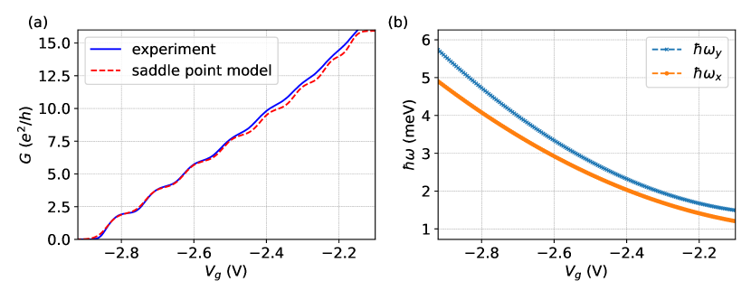
Finite-bias spectroscopy at zero field gives an estimate of the transverse confinement potential parameter from the variation of the subband spacings with (recall Fig. 2(d) in the main text). A good fit to a quadratic dependence of on is observed. The broadening parameter can be estimated by fitting the measured conductance at zero magnetic field to Eq. S4. Assuming a quadratic dependence of on , Fig. S3 shows the best fit (red) to the experimental curve (blue). We infer that a saddle-point potential is a good description of the constriction in the few-mode limit . The error in estimating the subband spacing in the many-mode limit may limit the applicability of the model for V. Furthermore, as seen in GaAs QPCs [3] the higher constriction density as the QPC is opened up leads to increased screening of the confinement potential, resulting in the transition from a harmonic confinement towards a flat-bottom potential well [4].
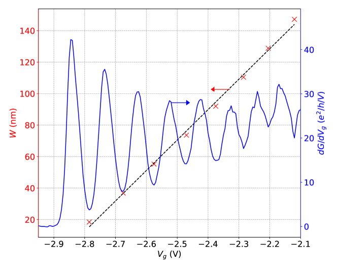
S6 Gate voltage dependence of constriction width
The constriction width as a function can be extracted from the conductance data at zero field, by recognizing at the -th transconductance minima, where is the Fermi wavelength in the 2DEG. Figure S4 shows the estimated which fits a straight line with slope nm/V.
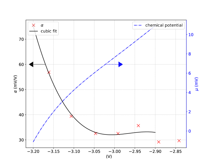
S7 QPC split-gate lever arm
The capacitive lever arm of the QPC gives the change in Fermi energy for 1 V change in . In other words, the lever arm quantifies the capacitive coupling between the split-gates and the constriction. Section III. 2 in the main text describes finite-bias spectroscopy on the QPC. The lever arm can be extracted as half the absolute slope of the transconductance maxima
| (S5) |
since half the diamond width along the axis corresponds to an energy scale equivalent to the full diamond height along the axis.
The chemical potential , defined as the Fermi level offset w.r.t. the conduction band edge can be expressed as
| (S6) |
where at the pinch-off gate voltage .
To translate the subband spin-splittings in an in-plane magnetic field from gate voltage (Fig. 3(a)) to chemical potential (Fig. 3(b)), we perform the following steps –
-
1.
Estimate the lever-arm from finite-bias measurements of Fig. 2(d) as described by Eq. S5.
-
2.
Note that the zero-field pinch-off gate voltage shifted from -2.845 V to -3.184 V between the finite-bias measurements in Fig. 2(d) and in-plane field measurements in Fig. 3(a). Offset the lever-arm to include for this conductance drift, , and fit a cubic polynomial to .
-
3.
Using Eq. S6 and V, evaluate .
Figure S5 plots the lever arm , from the first three spin-degenerate conductance plateau diamonds of Fig. 2(d), with a -0.339 V offset to include the conductance drift. Also shown is the cubic polynomial fit to , and the evaluated . The broadening of the transconductance peaks makes a precise estimation of challenging. We observe an expected decrease in as the constriction gets wider and the capacitive coupling reduces.
S8 In-plane magnetic field perpendicular to transport direction
The effective factor in-plane but perpendicular to the transport direction can be extracted by repeating the measurement described in Sec. III. 3 with a magnetic field in the -direction (see Fig. 1 for axes orientation). The transconductance as a function of and is shown in Fig. S6(a), with dark regions corresponding to conductance plateaus labeled in units of . Similar to the data from Fig. 3(a) in the main text, the Zeeman effect of the applied field breaks spin degeneracy and gives rise to odd-integer plateaus. The transconductance has local maxima when the source/drain chemical potential is in resonance with a subband edge. Conductance traces for T is shown in Fig. S6(e), with the expected emergence of conductance plateaus at and as is increased, and the corresponding decrease in the width of the even-integer plateaus.
As described in the main text and Sec. S7, the spin-splitting of the subbands is further elucidated in Fig. S6(b) by translating to chemical potential , using the split-gate lever-arm . A linear fit to the transconductance maxima, constrained to intersect at for each spin-split subband pair, is used to the extract the Zeeman energy as a function of , as depicted in Fig. S6(c). The in-plane factor extracted from the slope of the Zeeman energy is shown in Fig. S6(d), revealing negligible anisotropy between and directions. The error estimates are based on fitting parameter variances. See Sec. III. 4 in the main text for further discussion.
S9 Out-of-plane -factor in the 2DEG
The out-of-plane effective factor in the 2DEG can be extracted from the magnetoresistance measured in a Hall-bar with . The many-body exchange enhancement to the factor has its origins in the spin-population difference of Landau-levels. The enhancement depends on the Fermi level position, and is maximized at odd filling factors – which corresponds to the largest difference in spin-population. Furthermore, this many-body interaction is screened with increasing density, and consequently, a reduction in the oscillation amplitude is expected for higher filling factors.
Our approach for extracting is described in detail in Ref. 5. The four-terminal longitudinal resistance has a maximum whenever the Fermi level is in resonance with a spin-split Landau level. For a spin-split Landau level pair we have,
| (S7) |
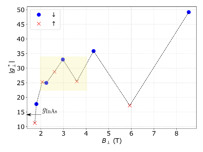
where is the bottom of the conduction band, is the 2DEG electron density, is the Landau level index, and is the out-of-plane magnetic field corresponding to each maxima. The extracted from the measured magnetoresistance (Fig. S1(c)) and Eq. S7 is depicted in Fig. S7. As discussed above, an oscillatory enhancement with successive depopulation of spin-split Landau levels is observed. The amplitude and mean value of the oscillations decreases towards the bulk value with increasing filling factor (decreasing field). The gigantic oscillations at low filling factor which decrease with field is strong evidence for many-body exchange interaction driven enhancement of . Interestingly, in the T range (yellow box in Fig. S7) used to study the 1D in the QPC (recall Fig. 4(d)) the enhanced factor of the 2DEG . This implies that the enhanced in the constriction, and the large anisotropy (Sec. III. 3, D) are driven by many-body interactions in the 2DEG.
S10 Notes on QPC stability and reproducibility
In this section we present data from various QPCs fabricated on the same heterostructure stack. The measurements were made over 9 cooldowns, intermittently over a period of 11 months. We focus on hysteresis and drift with fixed as well as bidirectionally swept over a range as the figures of merit.
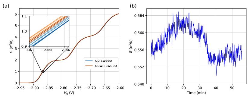
Figure S8(a) tracks the conductance through the QPC (the same QPC as in the main text) as the symmetric gate voltage was swept bidirectionally ten times in the range V. Sweeps in the same direction are ordered from light to dark trace. Hysteresis between up and down sweeps was mV and sweeps in the same direction fell within a 1 mV horizontal translation of one another. In Fig. S8(b), the QPC was set to a position along the first riser ( ) and the device conductance was watched for one hour. The variation in conductance remained within 1.5%. The stability in device operation allowed for longer sweeps such as the dc bias spectroscopy maps to be taken without additional tuning.
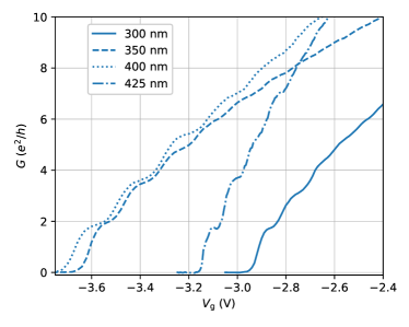
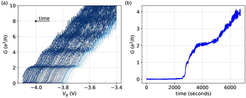
Conductance curves from four additional QPCs—fabricated on other mesas in the same fabrication run and measured over various cooldowns—are shown in Fig. S9. Multiple conductance plateaus are consistently seen in these constrictions, although there are variations in pinch-off voltage, width and flatness of the plateaus, and steepness of the risers. A frequent failure mode for our QPCs was leakage between the gates and the 2DEG. In addition, some QPCs showed cooldown-to-cooldown variation, especially in conductance stability versus time. Figure S10(a) shows conductance data from a separate cooldown from the same QPC as Fig. S8(a) and the main text while is swept bidirectionally in the range V. There is a persistent drift toward negative gate voltage with no indications of stabilizing. Figure S10(b) shows the conductance through the QPC with fixed at V, which begins in the pinch-off regime but drifts to finite conductance. Generally, we found the stability of the QPC to improve with time, with repeated back and forth sweeps in a limited voltage range, and with the application of moderate B-field.
References
- Steiger et al. [2011] S. Steiger, M. Povolotskyi, H.-H. Park, T. Kubis, and G. Klimeck, IEEE Transactions on Nanotechnology 10, 1464 (2011).
- Das Sarma and Hwang [2013] S. Das Sarma and E. H. Hwang, Phys. Rev. B 88, 035439 (2013).
- Geier et al. [2020] M. Geier, J. Freudenfeld, J. T. Silva, V. Umansky, D. Reuter, A. D. Wieck, P. W. Brouwer, and S. Ludwig, Phys. Rev. B 101, 165429 (2020).
- Laux, Frank, and Stern [1988] S. Laux, D. Frank, and F. Stern, Surface Science 196, 101 (1988).
- Raymond et al. [1985] A. Raymond, J. Robert, C. Bousquet, W. Zawadzki, F. Alexandre, and I. Masson, Solid State Communications 55, 271 (1985).