[a]Oak Ridge National Laboratory, Oak Ridge, Tennessee, USA \affiliation[b]University of Tennessee, Knoxville, Tennessee, USA \affiliation[c]Berea College, Berea, Kentucky, USA \emailAddcianciolotv@ornl.gov
A Novel Silicon Photomultiplier Readout Architecture for Low-light Applications
Abstract
In this article we describe the photon detection readout electronics for the nEDM@SNS experiment. The chosen ”photon counting” architecture, which utilizes high-efficiency silicon photomultipliers (SiPMs) and is appropriate for low-light applications, allows the use of a relatively high SiPM operating voltage. This maximizes photon detection efficiency and minimizes gain/efficiency voltage-dependence while eliminating direct optical cross-talk.
Electronic detector readout concepts (solid-state), Photon detectors for UV, visible and IR photons (solid-state) \arxivnumber
1 Introduction
The nEDM@SNS experiment [1], organized around principles laid out by Golub and Lamoreaux [2], aims to measure the neutron electric dipole moment with unprecedented precision () in order to shed light on the source of charge-parity violation responsible for the generation of matter in the Universe immediately following the Big Bang [3, 4].
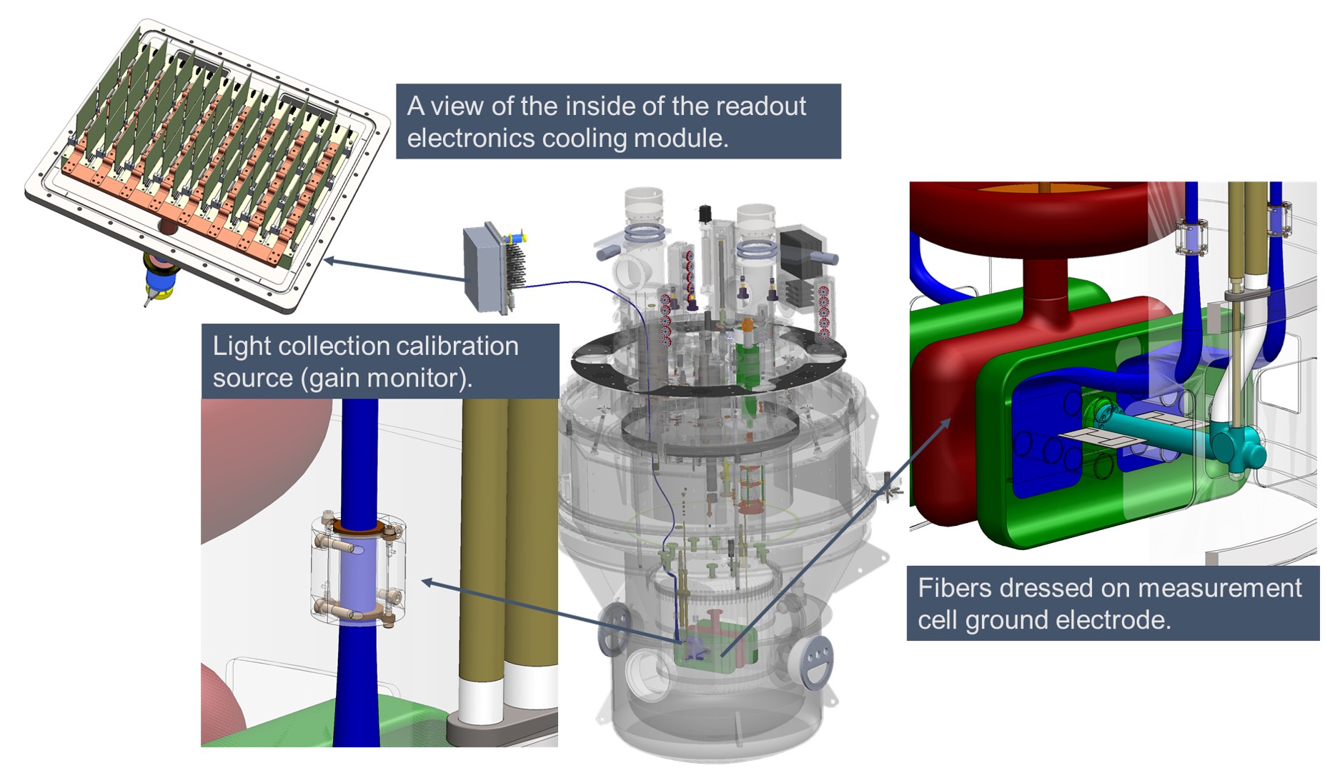
In this experiment ultracold neutrons are created and stored in a material trap (a ”measurement cell”) and exposed to highly uniform magnetic and electric fields. A non-zero electric dipole moment would alter the neutron precession by an amount proportional to the electric field. Neutron spin analysis is achieved by measuring the highly spin-dependent [5, 6, 7] rate of capture events. The resulting proton and triton produce 5,000 extreme ultraviolet (EUV; 80 nm) scintillation photons [8, 9, 10, 11, 12] when their energy is deposited in the surrounding superfluid helium bath. The EUV photons are converted to optical photons with a deuterated tetraphenyl butadiene coating on the surface of the measurement cell walls [13, 14], which are subsequently captured in wavelength-shifting fibers, and guided to an array of silicon multipliers (SiPMs) and associated readout electronics housed in a temperature-controlled chamber at -80 C outside the experiment’s magnetically shielded enclosure. Given sufficient stability in the light collection efficiency the number of detected photons can provide an in situ measurement of the volume-averaged electric field. Details of the nEDM@SNS light collection system and simulations of its expected performance can be found in [15].
Independent of SiPM choice, the SiPM readout architecture described here, appropriate for low-light applications, maximizes photon detection efficiency (), minimizes voltage and temperature dependence of and gain, and eliminating direct optical cross-talk.
2 Design Considerations
Energy Resolution: The He capture signal is monoenergetic and thus produces a fairly sharp peak in the number of photons detected per event. In contrast, background events111The primary background source is neutron -decay. Other sources include Compton-scattered -rays (originating from neutron activation of nearby materials as well as ambient sources) and cosmic rays. have fairly broad distributions. To achieve the target sensitivity, capture events must be detected with high efficiency () and the majority of -decay background events must be rejected () [1, 15]. Rejection of background events is achieved by applying a window cut on the signal peak in the detected photon spectrum, the effectiveness of which is set by the energy resolution.
Gain Stability: Liquid helium scintillation photon yield is reduced in the presence of an electric field which can prevent electrons and ions (produced by ionizing energy loss) from radiative recombination [10, 11, 12]. As a consequence, a precision measurement of the photon yield provides an elegant in situ measurement of the average electric field [16]. At the design operating field ( kV/cm) the scintillation yield dependence on the field can be approximated by . Thus, to measure the electric field with 1% accuracy requires measuring the scintillation yield with 0.18% accuracy. Long-term gain drifts (for instance, due to degradation of the WLS measurement cell coating) can be separated from electric field drifts through periodic field-off gain calibration runs.
Dark Rate: Thermal generation of charge carriers in the photosensors (dark rate) produces temporally random single-photoelectron-equivalent background events. High dark rate can produce accidental coincidences. Accidental coincidences between multiple dark rate pulses increases the trigger rate and can produce false n+3He capture signals. Accidental coincidences between dark rate pulses and scintillation events within the characteristic time of prompt EUV photon emission degrades the energy resolution. Accidental coincidences between dark rate pulses and scintillation events within the characteristic time of non-prompt EUV emission reduces background rejection capability [17], and this sets the most stringent requirement of the rate ( kHz/cell).
Separation of Photon Generation/Detection: The EUV scintillation photons are produced in a challenging environment ( K, kV/cm). In addition, the region near the measurement cell has strict non-magnetic requirements and every penetration of the outer vacuum vessel (which serves as a Faraday cage), especially by a condutor, represents a potential noise source that can interfere with the experiment’s SQUID magnetometers [18]. The closest acceptable location for the photosensors is several meters distant from measurement cells, outside the Faraday cage and the Magnetic Shield Enclosure, see Figure 1.
3 Design and Implementation Details
Overview: The long distance and tortuous path between photon generation and detection led to the choice of optical fiber light guides. After being converted to visible wavelengths the scintillation light is collected inside 192 0.5 mm diameter wavelength-shifting (WLS) fibers pressed against the measurement cell wall adjacent to the ground electrode. Because of the relatively short transmission length of WLS fibers (compared to clear, undoped fibers) both ends of each WLS fiber are mated to clear fibers close to the measurement cell.
The light guides transport the photons to an array of Silicon Photomultipliers (SiPMs) - one SiPM per WLS fiber end. Energy resolution places a premium on photon detection efficiency (), making SiPMs a natural photosensor choice [19]. This is especially true given that a fiber is smaller than an individual SiPM, avoiding any inter-SiPM geometric inefficiency.
We follow Otte et al. [25] and characterize SiPM performance as a function of relative over-voltage (), where is the operating voltage and is the breakdown voltage. This variable is convenient because the probability of breakdown can be described using a single parameter: .
Photon detection efficiency () increases with . dependence on (and thus temperature) decreases with (the two are closely related by the strong temperature dependence of , and thus when is fixed). These benefits must be weighed against two negative effects which both increase with : dark rate (for which the most stringent limit is set by a desire to measure non-prompt scintillation photons which may provide improved rejection of background events) and direct optical cross-talk (which works against the energy resolution improvement).
Dark rate can be easily reduced by cooling the SiPMs. Direct optical cross-talk is eliminated with a ”photon counting” readout architecture which uses a non-retriggerable voltage discriminator to produce a uniform voltage pulse when a SiPM is struck. Single photoelectrons can be cleanly identified above the electronic noise pedestal, so single photoelectron signals can be selected with efficiency. The discriminator is dead for the duration of its output pulse (chosen to be ns), so direct optical cross-talk ignored since direct optical photons occur immediately following the primary photon interaction in the SiPM. Delayed optical cross talk and SiPM afterpulsing events can occur up to 100 ns after the primary photon interaction in the SiPM, but most of these events are also eliminated by the dead window. Those which remain will not contribute to the determination of the energy of the prompt scintillation pulse. Those that remain can be clearly separated from the non-prompt scintillation light due to their short time constant. The dead window introduces inefficiency when multiple scintillation photons from the same event hit the same SiPM, but in the prevailing low-light conditions this rarely happens. The photon counting readout architecture also has the benefit of eliminating any impact from SiPM gain variation.222SiPM gain variation can result from sensor-to-sensor differences in intrinsic gain, or temperature. By producing a digital output ”photon counting” ignores these variations, assuming the gain is high enough that a single photoelectron is well above the discriminator threshold. Signals from 16 SiPMs are multiplexed into a single readout channel whose output is a voltage pulse with amplitude proportional to the number of photons detected on those SiPMs. Thus each channel provides a count (from 0 to 16) of the number of struck SiPMs. Note, for an average signal we expect struck SiPM per channel.
Fiber choice: Kuraray Y-11 fibers [20] have been thoroughly characterized by multiple experimental groups [21, 22, 23]. The Y-11 absorption spectrum has good overlap with the TPB emission spectrum [13, 14], and the Y-11 emission spectrum is peaked near 500 nm, well-suited for many SiPMs. Double-cladded fibers have superior capture fraction (10.8%). The S-type is resistant to cracks (minimum bend diameter fiber diameter) and we have observed no degradation in performance following numerous thermal cycles. Simulations [15] show standard dye density (200 ppm) and fiber diameter (either 0.5 or 1 mm) are appropriate.
We transition to clear fibers (ESKA SK-40, 1 mm diameter [24]) to maximize transmission over the relatively long distance ( m) to the photosensors.
Photosensor choice: Various types of silicon sensors have high photon detection efficiency. SiPMs were chosen due to their conveniently low operating voltage ( V) and superior energy resolution which allows clean identification of single photoelectrons. Otte et al. [25] carried out extensive performance characterizations of SiPMs from FBK (NUV-HD), Hamamatsu (S13360-3050CS), and SensL (J-Series 30035). Hamamatsu sensors were shown to have higher (especially at green wavelengths), a wider vs. plateau, and lower dark rate. We selected the Hamamatsu S13360-1375CS [26] - a different package of the same family of sensors tested in [25] with smaller area and larger pixel size. The smaller area (1.3 mm 1.3 mm) is optimal for reading out a single fiber, and the larger pixel size (75 m) increases 20% due to increased geometric efficiency (the resulting reduction in dynamic range is irrelevant at our low light levels).
One concern with the Hamamatsu sensors was the large range of ( V) listed in the product datasheet. Without a separably tunable for each SiPM, variations result in variations that lead to reduced (in sensors with higher ) and higher dark rate (in sensors with lower ). Sensor-dependent values also worsen the signal peak resolution.
Otte et al. [25] showed that as a function of is well described by
| (1) |
where for Hamamatsu sensors exposed to photons between 500-589 nm. The expected mean number of photoelectrons in a He signal event is 17 [15], giving a shot-noise limited signal peak resolution of . To prevent sensor variations in from contributing significantly to the signal peak resolution we require sensor-to-sensor variations to be an order of magnitude smaller than this: . At an operating voltage such that , and . For the Hamamatsu sensors V, leading to the requirement that V333Otte et al. [25] found mV/C for the Hamamatsu sensors, so the uniformity requirement leads to a modest temperature uniformity requirement: C. and making V variations unacceptable. However, Hamamatsu guaranteed and delivered 1,000 sensors within V of the nominal at no extra cost.444The quoted value is presumably a batch-to-batch variation rather than variation within a batch. It follows immediately that such variations do not contribute significantly to efficiency loss. Otte et al. [25] studied the dark rate dependence on both and temperature. Sensors with 0.75 V below nominal will have above nominal, corresponding to a 15% increase in the dark rate. This modest increase is easily mitigated by reducing the SiPM temperature C.
Operating temperature: Otte et al. [25] found that the Hamamatsu sensor dark rate was kHz/mm2 at , and T= -40 C and had a strong temperature dependence: at fixed , .555Dark rate temperature dependence in Figure 23 of Otte et al. is plotted vs. . Dependence vs. is obtained from Equation 13 and fit parameters given in Table 2 of the same reference. We have 384 sensors per cell, for a total sensor area of mm2, so for kHz/cell we require C. With this dark rate the contribution of false hits to the prompt scintillation pulse (width ¡ 100 ns) will be negligible (), as will the false trigger rate (1.6 Hz, assuming a simple double coincidence).
Voltage and temperature stability: The photon counting technique reduces the system gain ( = charge per photon) stability requirement to a photon detection efficiency stability requirement since each detected photon outputs the same charge: . In the discussion following Equation 1 we showed that at our operating voltage , from which the voltage stability requirement can be derived: , or mV, since V. This imposes requirements on both and . Commercially available supplies [27] easily achieve the required stability. The stability requirement is effectively a temperature stability requirement: C.
It is worth noting that without photon counting the system gain stability requirement applies to the product of the photon detection efficiency and the SiPM analog gain (). Otte et al. [25] showed for the Hamamatsu sensors. So, to achieve would require . With V and this gives mV, significantly more stringent than required with the photon counting technique.
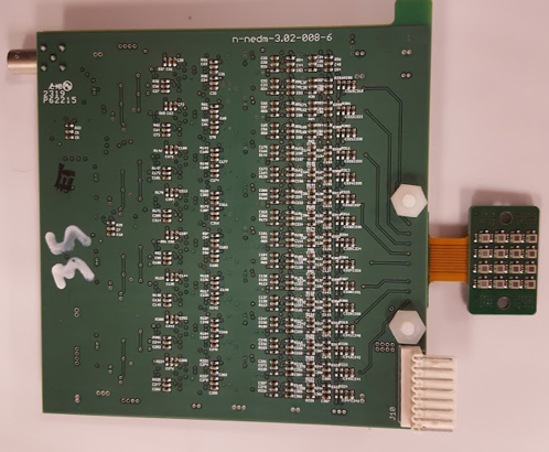
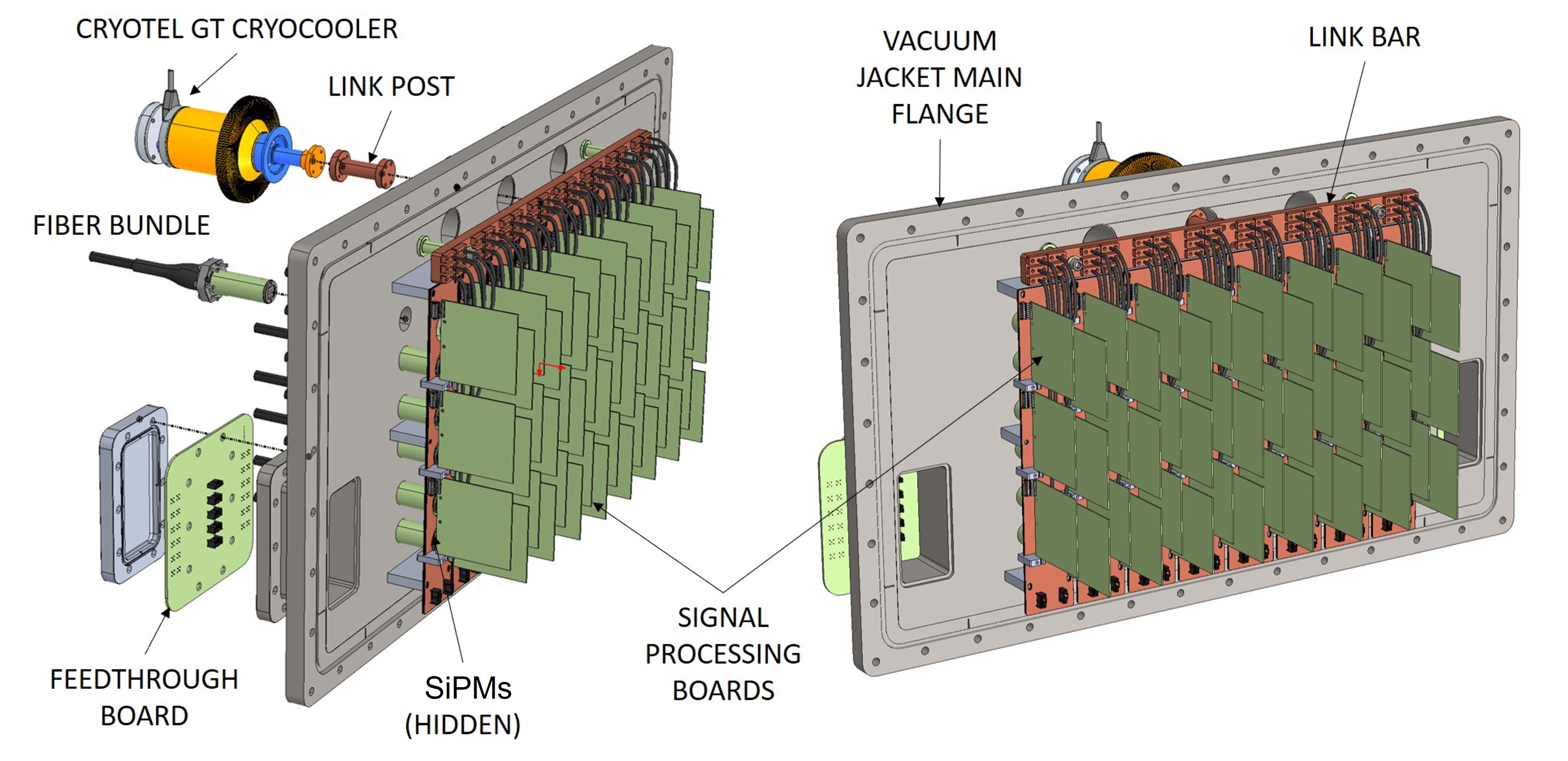
Circuit details: 16 SiPMs are mounted on a rigid-flex circuit and connected to a PCB with the signal processing circuitry (see Figure 2). The flex circuit connection between the two boards simplifies the cooling geometry, as described below.
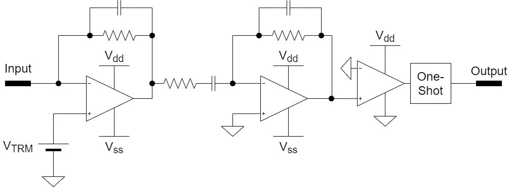
Each SiPM has a dedicated readout circuit (see Figure 3), the function of which is to identify whether a photon was detected by the SiPM. This circuit takes advantages of the extremely high signal-to-noise ratio resulting from the small area and low-capacitance of the SiPMs, which allows use of a commercial operational amplifier as a front-end device without excessive concern about electronic noise. The operational amplifiers were chosen based on low noise, low power, adequate bandwidth, and the ability to correctly function at cryogenic temperatures. Texas Instruments’ OPA 836 [28] has a quiescent current of only 1 mA from a symmetric 2.5 V rail and yet has a noise of 4.6 . The dynamic response is outstanding with a 205 MHz bandwidth and a fast rise time with rail-to-rail outputs. This component is specified for an operating range of -40 C to +125 C, but successful tests were performed at liquid nitrogen temperature (77 K) establishing good performance at cryogenic temperatures. The use of an operational amplifier as the front-end element has the added advantage of allowing fine trimming of the SiPM bias (when DC coupled, as is our case) by shifting the DC value at the non-inverting port. 666See voltage source VTRM in Figure 3. Since the sensors delivered by Hamamatsu had sufficiently uniform we did not need to take advantage of this feature. Photon detection is registered by a low-power comparator with a fixed threshold and proper hysteresis. Once the signal presence is detected a custom, fast, non-retriggerable one-shot shapes its duration to a selectable width. The reason for a custom one-shot is that commercial devices do not reliably allow output pulse widths less than 75 ns. In order to minimize dead time associated with the photon counting process we required a pulse width of 50 ns. The digital TTL response of the 16 one-shots on a processing board are converted to a pre-determined analog amplitude, and summed in an analog fashion into an inverting amplifier that provides a single output for all 16 SiPMs. It should be noted that, if signal rates are low enough this architecture allows each SiPM, or group of SiPMs, to be effectively encoded in both pulse duration and pulse amplitude to provide unequivocal identification of struck SiPMs if needed.
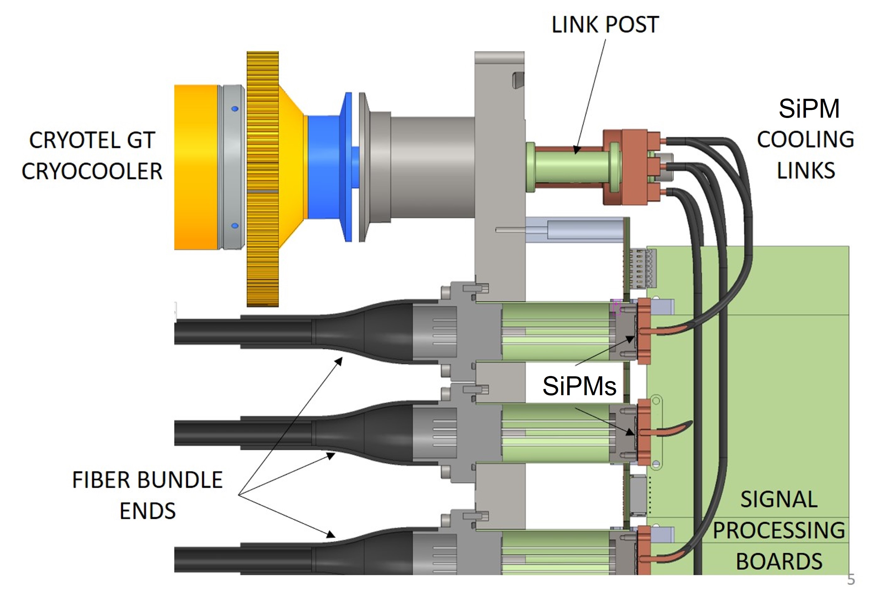
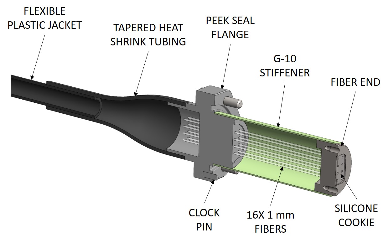
Cooling details: The goal of the SiPM readout cooling system is to keep the SiPMs at or below -80 C, with temperature stability on the order of 1-2 C and uniformity within C. To achieve these goals the SiPMs are mounted in a vacuum enclosure and thermally anchored to a 16 W Cryotel GT cryocooler [29]. The basic geometry of the cooling system is shown in Figure 4. The primary conductive heatloads to the SiPMs are from the associated fiber light guide (0.11 W) and processing board (0.14 W). The heatload from the fiber light guide is minimized by the design shown in Figure 5 which limits the area of the conductive pathway to that of the fibers themselves plus that of the G-10 stiffener. In addition to the W conductive load the cryocooler must remove an additional 5.8 W, primarily due to radiative heating. The thermal performance of the system has been modeled with ANSYS, with pressed joint conductances calculated using a rough model from [30] Calculations show a comfortable amount of extra cooling capacity and temperature uniformity well within the C goal. The temperature uniformity requirement translates to a heatload uniformity requirement. Increased heatload results in increased temperature of the cryocooler heat exchanger and reduced temperature drops across the thermal links. Given the cryocooler cooling curve and the design thermal link conductances one finds , so the heatload must be stable to within W. The heatloads, and therefore the temperature, are expected to be quite constant (the vacuum enclosure is in a temperature controlled experimental hall and the signal processing board current draw is fixed). But the system will be instrumented with two 25 W resistive heaters and thermometry on a subset of SiPM boards, so active control can be implemented if needed.
4 Performance
The performance of the SiPMs and associated readout electronics was evaluated by mounting each 16-channel readout unit in a cold box (Delta 9023) maintained at -60 C. The SiPMs were illuminated by Kuraray Y-11 fibers, each of which could be independently pulsed with an LED. The pulse size was set so that the average number of photons per pulse was much less than one to guarantee that all effectively every signal above the pedestal corresponded to a single photoelectron. Both the digital output and a diagnostic analog output from each readout unit were fed into a CAEN DT5730B waveform digitizer.
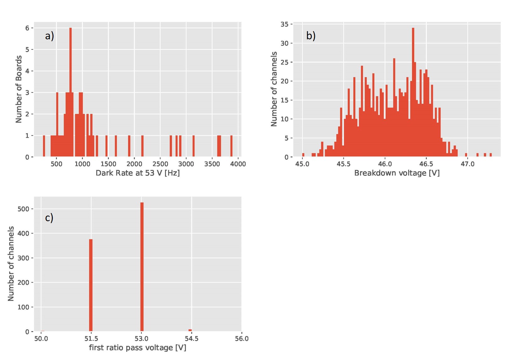
The dark rate was measured for each readout unit, as shown in Figure 6a. The average rate per board (total SiPM area ) is Hz, in line with expectations from Otte et al. [25] at this temperature. Outliers may be due to imperfections in screening ambient light. If not, there are sufficient spares to avoid using the noisier SiPMs. By running at somewhat lower temperature (-77 C) we can meet the desired dark rate of 4 kHz/cell (twenty-four 16-channel readout units).
The breakdown voltage for each SiPM, plotted in Figure 6b was determined by pulsing individual SiPMs at a variety of settings, integrating the resulting analog pulses, plotting the average single photoelectron signal size (i.e., the gain) vs. , and finding the -intercept of a linear fit to the results. All but a few sensors are within Hamamatsu’s V guarantee. All are well within our V requirement.
Finally the performance of the discriminator circuit was evaluated by testing for the presence of a digital signal when a single photoelectron analog signal was present. Figure 6c shows the distribution of settings where the boards first achieved 95% efficiency on the digital signal. All but one board had full efficiency at or below the nominal setting (53 V).
5 Conclusions
We have developed and successfully tested nearly 1,000 channels of Silicon Photomultiplier readout electronics for the nEDM@SNS experiment. The ”photon counting” architecture provides many advantages for low-light applications and the design is generic enough that it may find use in other similar applications.
We gratefully acknowledge the support of the U.S. Department of Energy Office of Nuclear Physics through grant DE-AC05-00OR22725.
References
- [1] M. W. Ahmed et al., A New Apparatus for a Cryogenic Measurement of the Neutron Electric Dipole Moment, J. Inst. 14 (2019) P11017.
- [2] R. Golub and S. K. Lamoreaux, Neutron Electric-dipole Moment, Ultracold Neutrons and Polarized 3He, Phys. Reports 237 (1994) 1.
- [3] A. Sakharov, Violation of CP Invariance, C Asymmetry, and Baryon Asymmetry of the Universe, J. Exp. Theo. Phys. Lett. 5 (1967) 24.
- [4] P. Schmidt-Wellenburg, The Quest to Find an Electric Dipole Moment of the Neutron, AIP Conf. Proc. 1753 (2016) 060002.
- [5] L. Passell and R. I. Schermer, Measurement of the Spin Dependence of the Reaction and of the Nuclear Susceptibility of Adsorbed He3, Phys. Rev. 150 (1966) 146.
- [6] S. B. Borzakov et al., Features of the departure from the law of the cross section for the reaction . Excited level of the 4He nucleus. Sov. J. Nucl. Phys. 35 (1982) 307.
- [7] C. D. Keith et al., Neutron cross sections for 3He at epithermal energies, Phys. Rev. C 69 (2004) 034005.
- [8] E. H. Thorndike and W. J. Shlaer, Rev. Sci. Instrum. 30, (1959) 838.
- [9] H. Fleishman, H. Einbinder, and C. S. Wu, Rev. Sci. Instrum. 32, (1961) 1173.
- [10] T. M. Ito et al., Effect of an electric field on superfluid helium scintillation produced by -particle sources, Phys. Rev. A 85, (2012) 042718.
- [11] T. M. Ito and G. M. Seidel, Scintillation of Liquid Helium for Low-Energy Nuclear Recoils, Phys. Rev. C 88, (2013) 025805.
- [12] N. S. Phan et al., Effect of an electric field on liquid helium scintillation produced by fast electrons, Phys. Rev. C 102 (2020) 035503.
- [13] D. N. McKinsey et al., Detecting Ionizing Radiation in Liquid Helium Using Wavelength Shifting Light Collection. Nucl. Instrum. and Meth. A 516 (2004) 475.
- [14] V. M. Gehman et al., Characterization of protonated and deuterated Tetra-Phenyl Butadiene Film in a Polystyrene Matrix, J. Inst. 8, (2013) P04024.
- [15] D. Loomis, V. Cianciolo and J. Leggett, Simulations of the nEDM@SNS light collection system efficiency, J. Inst. 17 (2022) T04007.
- [16] S. Clayton and T. M. Ito, private communication.
- [17] D. N. McKinsey et al., Time Dependence of Liquid-Helium Fluorescence, Phys. Rev. A 67 (2003) 062716.
- [18] Y. Kim and S. Clayton, Tests of a SQUID-based He-3 co-magnetometer readout for a neutron EDM experiment, IEEE Trans. Appl. Supercond. 25 (2015) 1600205.
- [19] S. Gundacker and A. Heering, The silicon photomultiplier: fundamentals and applications of a modern solid-state photon detector, Phys. Med. Bio. 65 (2020) 17T01.
- [20] Kuraray Plastic Scintillating Fibers, \hrefhttp://kuraraypsf.jp/psf/index.htmlhttp://kuraraypsf.jp/psf/index.html
- [21] D. S. Ayres et al., The NOvA Technical Design Report, Report No. FERMILAB-DESIGN-2007-01.
- [22] E. C. Dukes et al., Performance of wavelength-shifting fibers for the Mu2e cosmic ray veto detector, J. Inst. 13 (2018) P12028.
- [23] W. Bugg, Yu. Efremenko and S. Vasilyev, Large Plastic Scintillator Panels with WLS Fiber Readout; Optimization of Components, Nucl. Inst. Meth. A 758 (2014) 91.
- [24] ESKA GK-40 Datasheet, \hrefhttp://www.princetel.com/datasheets/ESKA_GK-40.pdfhttp://www.princetel.com/datasheets/ESKA_GK-40.pdf
- [25] A. N. Otte et al., Characterization of Three High Efficiency and Blue Sensitive Silicon Photomultipliers, Nucl. Inst. Meth. A. 846 (2017) 106.
- [26] Hamamatsu MPPC S13360/S13362 series, \hrefhttps://www.hamamatsu.com/us/en/product/optical-sensors/mppc/mppc_mppc-array/index.htmlhttps://www.hamamatsu.com/us/en/product/optical-sensors/mppc/mppc_mppc-array/index.html
- [27] e.g., BK Precision 1787B: \hrefhttps://www.bkprecision.com/power-supplieshttps://www.bkprecision.com/power-supplies
- [28] TI OPA836 Datasheet: \hrefhttps://www.ti.com/lit/gpn/opa836https://www.ti.com/lit/gpn/opa836
- [29] Cryotel GT Cryocoolers: \hrefhttps://www.sunpowerinc.com/products/stirling-cryocoolers/cryotel-cryocoolers/gthttps://www.sunpowerinc.com/products/stirling-cryocoolers/cryotel-cryocoolers/gt
- [30] R. F. Barron and G. F. Nellis, Cryogenic Heat Transfer, Second Edition, CRC Press, Taylor & Francis Group (2016).