Also at ]Department of Materials Science and Engineering, University of Tennessee, Knoxville, TN, USA, 37996
Memristor Compact Model with Oxygen-Vacancy Concentration as State Variable
Abstract
We present a unique compact model for oxide memristors, based upon the concentration of oxygen vacancies as state variables. In this model, the increase (decrease) in oxygen vacancy concentration is similar in effect to the reduction (expansion) of the tunnel gap used as a state variable in existing compact models, providing a mechanism for the electronic current to increase (decrease) based upon the polarity of the applied voltage. Rate equations defining the dynamics of state variables are obtained from simplifications of a recent manuscript in which electronic processes (i.e., electron capture/emission) were combined with atomic processes (i.e., Frenkel pair generation/recombination, diffusion) stemming from the thermochemical model of dielectric breakdown. Central to the proposed model is the effect of the electron occupancy of oxygen vacancy traps on resistive switching dynamics. The electronic current is calculated considering Ohmic, band-to-band, and bound-to-band contributions. The model includes uniform self-heating with Joule-heating and conductive loss terms. The model is calibrated using experimental current-voltage characteristics for \ceHfO2 memristors with different electrode materials. Though a general model is presented, a delta-shaped density of states profile for oxygen vacancies is found capable of accurately representing experimental data while providing a minimal description of bound to band transitions. The model is implemented in Verilog-A and tested using read/write operations in a 4x4 1T1R nonvolatile memory array to evaluate its ability to perform circuit simulations of practical interest. A particular benefit is that the model does not make strong assumptions regarding filament geometry of which scant experimental-evidence exists to support.
I Introduction
Several physics-inspired compact models have been proposed for circuit-simulation of oxide memristors–key elements for emerging applications in non-volatile memories, unconventional computing, and biologically-inspired computing alike raj_memristor_2021 ; du_low-power_2021 ; sun_hybrid_2010 ; thomas_memristor-based_2013 ; lu_biological_2020 . These are largely based on assumptions regarding the geometry of a “conductive filament”, described either in terms of a one-dimensional tunnel gap chen_synapse_2013 ; zhang_memristive_2017 ; vourkas_spice_2015 ; guan_SPICE_2012 ; chen_compact_2015 or the size/shape of the filament approximated as cylindrical bocquet_robust_2014 or rectangular biolek_spice_2009 ; kvatinsky_team_2013 . Electronic conduction processes–derived from changes in filament geometry–are usually modeled with drift/diffusion gao_oxide-based_2008 ; larentis_resistive_2012 ; gilmer_asymmetry_2012 ; vandelli_modeling_2011 ; nardi_resistive_2012 , hoppinghuang_physics-based_2013 , trap-assisted and band-to-band tunnelingguan_SPICE_2012 , Poole-Frenkel emission, site-percolationsune_new_2001 ; sune_analytical_2009 ; tous_compact_2010 ; long_compact_2013 , or interfacial redox reactions bocquet_robust_2014 . Additionally, conduction models sometimes incorporate simple thermal models (e.g., uniform Joule heating) since local temperature is purported to have a significant impact on electrical characteristics, particularly retention kumar_Conduction_2016 and multibit operation alexandrov_current-controlled_2011 .
The scope of existing tunnel-gap models can be understood simply by taking any or all of the nominal conduction processes present in metal-insulator-metal devices (e.g., direct and Fowler-Nordheim tunneling, thermionic emission, Poole-Frenkel emission, Ohmic conduction, ionic conduction and space-charge limited conduction sze_physics_2006 ) and replacing the insulator thickness parameter with a dynamic variable (i.e., the tunnel gap) ranging from zero to a few nanometers guan_SPICE_2012 . The dynamics of the tunnel gap are based on the diffusion kinetics of oxygen ions presumed to be rate-limiting–approximated in one-dimension along the oxide thickness using the Mott-Gurney drift velocity yu_Phenomenological_2010 . A positive voltage drives ions towards the top electrode, reducing the tunnel gap; a negative voltage drives ions towards the bottom electrode, increasing the tunnel gap. Since this implicitly assumes Frenkel pairs recombine (generate) in the presence (absence) of oxygen ions, the thermal barriers for recombination/generation must be smaller than that of oxygen ion diffusion wherever the model is applied so as not to become rate-limiting. The zero-field thermal barrier for Frenkel pair generation can be (at grain boundary sites aldana_Resistive_2020 ), (at gettering electrode surfaces xu_Kinetic_2020 ) and several electronvolts in the bulk ( aldana_Resistive_2020 , xu_Kinetic_2020 ) all of which are much larger than that of oxygen ion diffusion ( kumar_Conduction_2016 ). Consequently, tunnel gap models are adequate for describing reset or set operations jiang_Verilog_2014 ; guan_SPICE_2012 ; yu_Phenomenological_2010 particularly when the top electrode can be regarded as an oxygen reservoir with permeable interface and the electric field is large enough (tunnel gap small enough) that the thermal barrier for Frenkel pair generation is reduced and no longer rate-limiting. A more complex or entirely new framework would be required to incorporate a physical description of forming self-consistently within this model guan_Switching_2012 . Given that oxide memristors are flux driven chua_Memristorthe_1971 , a description which takes into account the entire electrical history of the device (forming, reset and set) is critical from a self-consistent physical modeling perspective.
It is important to note that all compact models are phenomenological, involving many simplifications to enable circuit simulation at various levels of complexity and computational efficiency. Ultimately, the accuracy and speed of the device compact model is selected based on the needs of the circuit designer rather than the physical accuracy alone. For example, simple piecewise linear models may be desired when the focus is on developing larger neuromorphic systems amer_practical_2017 whereas predictive physics-based models may be desired for testing smaller memory array architectures pickett_switching_2009 . Ideally, memristor compact models would stem from a common physical framework in which complexity can be selectively refined at the circuit level, similar to the different levels of the well-known SPICE models for conventional bulk MOSFETs (square law, bulk charge, etc.).
In this work, a compact model for oxide memristors is presented that is based on the concentration of oxygen vacancies and their electron occupancy as opposed to one-dimensional filament geometry. The shift from a tunnel gap to a concentration state variable may be more physically appropriate, given that the formation of a one-dimensional defect chain is statistically unlikely considering other competing factors such as vacancy diffusion, thermophoresis kumar_Conduction_2016 and the increased thermodynamic stability of defect clusters bradley_ElectronInjectionAssisted_2015 expected to lead to additional conduction pathways. These, along with the presence of grain-boundaries and other imperfections which may reduce the zero-field formation enthalpy of oxygen vacancies suggest a variety of filament shapes with varying connectivity as seen in comprehensive modeling approaches aldana_3D_2017 ; guan_Switching_2012 ; zeumault_tcad_2021 and experimental observations li_Direct_2017 .
In our model, the oxygen vacancy concentration is split into two state variables to allow the electron-occupancy of the vacancies to vary between occupied and unoccupied depending on electron capture and emission processes. This is based on recent KMC modeling approaches zeumault_tcad_2021 and reflects ab-initio calculations showing increased thermodynamic stability of negatively-charged oxygen vacancies under conditions of electron-injection bradley_ElectronInjectionAssisted_2015 as well as experimental observations of a negative-space charge associated with suspected filament regions li_Direct_2017 . This has immediate implications on retention, since a larger thermal emission barrier would result in a more stable low resistance state and therefore, longer retention time as we show by comparison to experimental data of memristors having different electrode materials. The compact model is implemented in Verilog-A, using simplifying assumptions made to our previous model zeumault_tcad_2021 . In particular, a key approximation is that the field-dependence of the microstate transitions is approximated using the average electric field as opposed to the local electric field. Since electron capture and emission processes are taken into account, the model utilizes additional parameters associated with the electrodes (e.g., work function, effective mass) and those of the oxygen vacancy defects (e.g., trap energy level/ionization energy, capture cross-section, and thermal capture barrier) that are intimately connected to the resistive switching dynamics. The model also considers temperature effects and, most importantly, does not assume a particular filament shape, gap size between filament tip or any other restrictive geometrical constraints which are not firmly supported by experimental data. Each of these features make this compact model attractive due to its predictive modeling capability and pairing ability with ongoing experimental investigations to identify and observe filament geometries kumar_Conduction_2016 ; li_Direct_2017 . Being generally based upon a concentration of defects as opposed to a particular filament geometry, the model is open to different interpretations of conduction (e.g., drift/diffusion, trap-assisted-tunneling or percolation) as we show.
Lastly, the treatment of oxygen vacancies as an electron trap allows the material-specific density of states to be specified to provide increased accuracy/reduced efficiency (continuous energy dependence) or decreased accuracy/increased efficiency (discrete trap level) based on the particular needs of the circuit designer. The density of states is more intimately connected to materials chemistry than is a tunneling gap, allowing greater flexibility when comparing model predictions to experimental data (e.g., defect spectroscopy thamankar_Single_2016 ). For circuit-simulation, a delta density of states profile is least mathematically complex to implement, requiring no numerical integration at each time step. Thus we extensively evaluate the compact model (implemented in Verilog-A) based on a delta profile density of states. The model is validated using independent experimental data-sets having different electrode materials and tested using a simple 4x4 1T1R array representative of a small nonvolatile memory array to evaluate the model’s capability to perform basic circuit simulations.
II Compact Model Framework
II.1 General Assumptions and Notation
| Parameter | Description | Value and Unit |
|---|---|---|
| Elementary charge | ||
| Boltzmann constant | ||
| Reduced Planck constant | ||
| Ambient temperature | ||
| Relative permittivity | ||
| Attempt-to-escape frequency | ||
| Activation energy for Frenkel pair generation | ||
| Activation energy for Frenkel pair recombination | ||
| Ionization energy of oxygen vacancy defect | - | |
| Capture cross-section of oxygen vacancies | ||
| TE work function (\ceTi) | ||
| BE work function (\ceTiN) | ||
| TE electron effective mass (\ceTi) | ||
| BE electron effective mass (\ceTiN) | ||
| TE electron concentration (\ceTi) | ||
| BE electron concentration (\ceTiN) | ||
| Oxide electron effective mass (\ceHfO2) | ||
| Oxide molecular dipole moment (\ceHfO2) | ||
| Oxide bandgap energy (\ceHfO2) | ||
| Oxide electron affinity (\ceHfO2) | ||
| Effective band mobility (\ceHfO2) | ||
| Oxide specific heat capacity (\ceHfO2) | ||
| Addenda heat capacity (Device) | ||
| Oxide mass density (\ceHfO2) | ||
| Oxide thermal conductivity (\ceHfO2) | ||
| Site density (\ceHfO2) | ||
| Trap center (\ceHfO2) |
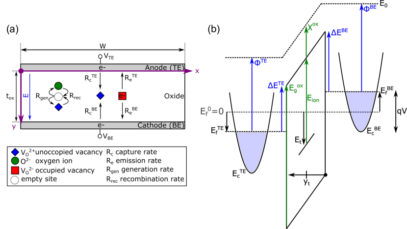
In Table 1, we define the notation for symbols used throughout the model as well as nominal material parameters for \ceHfO2 which we evaluate herein as the oxide material. In Figure 1, the device structure and definitions of energy levels are depicted. Although the model is presented using parameters for \ceHfO2, it is generally applicable to transition metal oxides of interest for memristors since it is based upon a general thermochemical model of dielectric breakdown mcpherson_thermochemical_2003 ; mcpherson_underlying_1998 , common to many insulating oxides and/or polar solids in general.
Below, we summarize the main assumptions used in deriving the compact model:
-
•
The oxide is single-phase (i.e., no polymorphism) with material properties of the single-crystalline bulk (e.g., effective mass, permittivity, bandgap, electron affinity). In practice, this implies the material properties are homogeneous and is not necessarily tied to the bulk crystalline or amorphous state.
-
•
The local electric field can be approximated with the spatially-averaged field.
-
•
Oxygen vacancies behave as electron traps (positive when empty , negative when occupied , accommodating 4 electrons bradley_ElectronInjectionAssisted_2015 ), defined in terms of a continuous electronic density of states to specify the ionization energies/defect levels participating in electron capture/emission.
-
•
The interface tunneling transmission probabilities for the top and bottom electrodes are approximately equal.
-
•
Diffusion of ionic point defects is not considered.
-
•
Trap to trap coupling is not considered.
II.2 State Variable Dynamics
The state of the oxide is represented using three species: unoccupied oxygen vacancies , occupied oxygen vacancies , and empty states ; each of these are taken to be volume-averaged quantities (i.e., concentrations). These are depicted in Figure 1(a). At any point in time, the sum of these is constant and equal to the total density of accessible sites, which is nominally equal to the atomic density of \ceHfO2 ().
| (1) |
We note that, in general, can be regarded as a parameter which establishes an upper bound for the state variables , , and . When is equal to the atomic density, the intrinsic state of the memristor is reachable in the absence of external current-compliance. As will be shown, reducing below the atomic density has a similar effect as forcing a current-compliance. A value of was used throughout this work based on agreement to experimental data.
From 1, since is a constant, the net rate of change in each species must sum to zero.
| (2) |
These rates can be expressed in terms of the following physical transitions: Frenkel-pair generation and recombination , electron capture and emission in which capture/emission of electrons can take place between either the top electrode (TE) or bottom electrode (BE).
The rate of change in electron occupancy of oxygen vacancy traps, due to electron capture and emission is given by Equation 3.
| (3) |
In terms of and the density of states , the occupied, unoccupied and total vacancy concentration can be calculated using Fermi-Dirac statistics.
| (4) |
| (5) |
| (6) |
Trap-to-trap coupling is neglected, which would otherwise give rise to a separate Fermi level for trap states and corresponding Fermi function for use in calculating trap concentrations. Instead, the number density of traps is used to compute the electron occupancy probability.
| (7) | ||||
| (8) |
Using these definitions, integration of Equation 3 over the density of trap states provides the rate equation for the occupied vacancy concentration ,
| (9) |
where is the normalized density of states profile for the oxygen vacancy levels.
| (10) |
Equation 9 simply states that unoccupied vacancy states are filled by either electrode (TE/BE) and occupied states are emptied to either electrode (TE/BE). The energy integral allows for the density of states to take on any energy dependence (e.g., delta, uniform, gaussian).
To account for defect creation, which initially gives rise to the formation of Frenkel pairs consisting of oxygen ions and unoccupied oxygen vacancies (i.e., , ), atomic processes are incorporated by assuming that the empty states in our model are increased (decreased) due to recombination (generation) of Frenkel pairs.
| (11) |
Using Equation 2, along with Equations 9 and 11, the remaining rate equation for the unoccupied vacancies is given by Equation 12.
| (12) |
Together, Equations 9, 11 and 12 define a dynamic relationship between atomic and electronic processes, which we have evaluated numerically in a recent manuscript in two dimensions, taking into account diffusion, Frenkel pair generation and recombination, electron capture and emission zeumault_tcad_2021 . For simplicity, the compact model developed here does not consider diffusion; diffusion of charged point-defects would produce a spatially and time-dependent electric field which would complicate compact model development.
II.3 Transition Rates
The rates and are atomic processes describing the creation and removal of Frenkel pairs of oxygen ions and vacancies (i.e., and ) whereas the rates and are electronic processes describing the capture and emission of electrons by oxygen vacancies, to either electrode.
The rates of Frenkel-pair generation/recombination can be described according to classical transition state theory, commonly applied in kinetic Monte Carlo simulations of oxide memristors.
| (13) | ||||
| (14) |
The thermal barriers for these transitions are electric field dependent (the local field can promote charge separation or recombination), which we model as a symmetric raising/lowering of the thermal barrier with field .
| (15) | ||||
| (16) |
These equations are implemented such that the maximum rate cannot exceed the exponential prefactor , occuring for high positive/negative voltages, otherwise leading to negative thermal barriers.
The capture rates can be described using a classical or quantum approach. The latter uses Fermi’s Golden Rule for the rate of interaction between the bound state (within the oxide) and the band state (within the electrode). For simplicity, the interaction potential can be confined to a box-shaped volume in which the interaction potential energy is set to the defect level referenced to the conduction band . For 2D or 3D modeling, in which spatially-dependent features are integral, a quantum approach may be desired for its improved accuracy. A complete derivation of both is provided in the supplementary material of our previous work zeumault_tcad_2021 and elsewhere jimenez-molinos_direct_2002 ; palma_quantum_1997 as implemented in standard device simulators synopsys_TCAD_2019 .
Equation 17 shows the resulting quantum model for an elastic transition.
| (17) |
An additional factor is included to account for the tunneling probability , using the Wentzel-Kramers-Brillouin (WKB) approximation for a triangular barrier of uniform field sze_physics_2006 . Here, is the Fermi-Dirac function, defined separately for each electrode; is the position of the trap relative to the electrode from which an electron is captured; is the electron effective mass of the electrode; is the trap volume; is a WKB tunneling parameter sze_physics_2006 . and can be expressed using a box-shaped potential for the trap state and a triangular barrier (uniform field) approximation for the conduction band as jimenez-molinos_direct_2002 ; palma_quantum_1997
| (18) | ||||
| (19) |
where is the conduction band offset at each electrode interface, is the electrode work function and is the electron affinity of the oxide; has two values, one for each electrode.
Equation 17 assumes that the interaction between bound states and band states is elastic, and that the electrodes can be approximated using a bulk parabolic band dispersion.
Here, for simplicity, we implement a classical model for the rate of interaction in terms of a capture cross-section, thermal velocity, carrier concentration and thermal barrier. The classical model has the same phenomenological aspects of the quantum model, though it differs quantitatively regarding the dependence on the trap level and applied voltage.
Regarding the in front of the field-dependent terms in Equation 20, the is used for the top electrode (TE) and the is used for the bottom electrode (BE). In either model, the emission rate to either electrode is calculated from the capture rates by the detailed balance criterion.
| (24) |
For the classical model, this leads to the following,
| (25) |
Regarding the in front of the field-dependent terms in Equation 25, the is used for the top electrode (TE) and the is used for the bottom electrode (BE).
The voltage dependence of these expressions enters via a symmetric raising/lowering of the Quasi Fermi energies from the equilibrium Fermi level (taken as zero, ) by amount such that the total difference between the Fermi-energies is .
| (26) | ||||
| (27) |
We note that, in general, transitions will be field-dependent; a field-dependence introduces a time-dependence for the rates since the local electric field strength is dependent upon the spatial arrangement of charged defects – which varies with time. For this reason, numerical modeling approaches require the solution to Poisson’s equation at each time-step as has been done elsewhere aldana_3D_2017 ; aldana_kinetic_2018 ; larcher_Microscopic_2012 ; zeumault_tcad_2021 . Towards compact-model development, as a simplification, everywhere the local field is replaced with the average field . Consequently, the rates depend on the applied voltage but not on time.
II.4 Electronic Conduction
The current-density is computed from the following components: band-to-band tunneling between electrodes , Ohmic conduction within the bands and bound-to-band tunneling from trapped electrons (i.e., trap assisted tunneling) . These are shown diagrammatically in Figure 1(b).
| (28) |
The band-to-band tunneling component accounts for Fowler-Nordheim tunneling through the thin, insulating portion of the \ceHfO2 sze_physics_2006 .
| (29) |
Alternatively, this can be refined with image-force correction using the general Simmons formula simmons_Generalized_1963 as in pickett_switching_2009 .
The Ohmic contribution is included based on charge neutrality considerations and considerations of information derived from prior literature. In our previous work, unoccupied oxygen vacancies were modeled as donors and occupied oxygen vacancies were modeled as acceptors zeumault_tcad_2021 . The charge-state of the vacancy changed each capture/emission event, since dynamic updating of the charge state of the system for each discrete transition is possible using a KMC approach. Throughout these processes, charge neutrality can be satisfied, using the space charge of oxygen ions and an additional compensating positive charge to balance the additional negative charge created due to the capture of electrons injected from the electrodes.
To illustrate, we consider a process leading to electron capture by an oxygen vacancy ( denotes a neutral site). Initially, Frenkel pair generation leads to neutral pairs of oxygen ions and oxygen vacancies .
| (30) |
After electron capture, negative oxygen ions remain, positive oxygen vacancies are removed and negative oxygen vacancies are created – producing a net negative space charge equal to per capture event (assuming 4 electrons are captured bradley_ElectronInjectionAssisted_2015 ).
| (31) |
Thus, by assuming that holes equal in concentration to are always present, bulk charge neutrality can be maintained within the oxide,
| (32) |
This assumes, that the oxygen ions are present throughout all processes behaving as negative fixed charges. However, oxygen ions can be removed or introduced into the oxide via gettering processes at the electrode interfaces, establishing a spatial dependence, and our model does not incorporate the oxygen ion concentration as a state variable. Instead of introducing a new state variable, we assume that an electron concentration equal to and a hole concentration equal to are always present within the bands to ensure charge neutrality. We note that, since the oxygen vacancy state is a deep level state, the binding energy is stronger and the electron/hole states are not expected to behave as weakly-bound, fully delocalized states with their respective band mobility, especially at high defect concentrations. Instead, we assume a single effective mobility parameter, with a drift current proportional to the total vacancy concentration.
| (33) |
Since this is a bulk component, it tends to become more important as the oxide thickness increases (reduced tunneling probability), as one might expect for highly defective insulators (e.g., \ceSiN_x); for thin films (), the tunneling current dominates. Note, we model the Ohmic conduction as a simple phenomenological model, using a constant effective mobility parameter. If desired, this can be further modified to be temperature and field-dependent using a Poole-Frenkel mobility model as in disordered media sze_physics_2006 .
| (34) |
Where , , , and are fitting parameters synopsys_TCAD_2019 . This is expected to be more significant for oxide memristors consisting of smaller bandgap oxides (e.g., \ceTiO2) presenting a smaller thermal barrier for local bound-to-band emission. However, it should be noted that, since Poole-Frenkel conduction is an additional emission component (to the bands within the oxide), the rate equation framework for the capture/emission process would need to be self-consistently modified if included, since all capture/emission processes effect the electron-occupancy of the oxygen vacancies. For simplicity, we do not consider such processes.
The trap-assisted-tunneling component is computed considering the current produced within a differential volume element centered about a discrete trap located within the oxide at schenk_advanced_1998 . In one dimension, we can write,
| (35) |
where is the net transition rate per unit volume, defined in terms of the electronic transition rates and density of states for traps , according to previous work zeumault_tcad_2021 .
| (36) |
Each electronic transition rate is position-dependent due to the tunneling factors. For a symmetric energy barrier at each electrode interface, the net transition rate will be maximum and sharply peaked for defects situated near the center of the oxide (the centroid of a uniform defect profile), regardless of the defect distribution. If the integral in Equation 35 can be approximated by its peak value, the spatial dependence can be eliminated. Replacing with yields the following,
| (37) |
This approximation effectively samples a narrow spatial range of the defect concentration (near the center of the oxide), regardless of the specific spatial distribution, since these will contribute more to the total integral in Equation 35.
II.5 Self Heating
Self-heating effects are approximated by assuming uniform Joule heating where the oxide volume dissipates heat via conduction to the external device temperature at .
| (38) |
Starting with an initial temperature , equal to the device temperature, the temperature at the next time step is given in terms of the instantaneous temperature , thickness , specific heat capacity , mass density , thermal conductivity of the oxide, current density , and ambient temperature .
| (39) |
Equation 39 is the numerical solution to the time-dependent heat equation in one dimension, considering Joule heating and conductive heat losses to the electrodes (Equation 38). The factor is due to the assumption that heat dissipates from the center of the device over a distance equal to half the oxide thickness (). The model is approximate and, in practice, the quantity is the specific thermal conductance and is a fitting parameter. Use of self-heating creates internal temperature as an additional state variable for each memristor and, since temperature is not intrinsically bound, requires a window function to prevent temperatures from reaching absurd values. However, dynamic inclusion of self-heating may not always be necessary. For example, in oxide memristors having thin dielectrics, primary electronic conduction involves coupling traps within the dielectric to nearby electrodes via tunneling. Tunneling current, by contrast, produces a boundary condition for the current density, as opposed to a local current density within the oxide. Joule heating is therefore expected to occur near the electrodes – where tunneling electrons dissipate their excess kinetic energy into the contacts which behave as thermal reservoirs. Thus, for simplicity, if the electrode can be treated as an efficient thermal reservoir, the dynamic effects of Joule heating might be approximated simply by observing how the model responds to static changes to the ambient temperature.
Close inspection of Equation 39 shows that the “device” is taken as the oxide volume. Since the oxide volume constitutes a svery mall fraction of the thermal system (see SEM image within zhang_Experimental_2011 ), a more realistic inclusion of self-heating considers that the oxide presents a negligible thermal mass in comparison to the electrodes and surrounding device structure which is much more efficient at conducting heat due to the lower thermal conductivity of the oxide. Without such a correction, inclusion of thermal models leads to absurdly high temperatures and/or nonsensical fitting parameters. For example, using the device geometry and thermal resistance () reported in one comprehensive modeling approach of \ceHfO2 memristors guan_Switching_2012 the effective thermal conductivity of the \ceHfO2 evaluates to , which is 100 times larger than the measured value panzer_Thermal_2009 . Equation 39 is therefore modified to include a correction factor that accounts for the addenda heat capacity due to the bulkier elements in thermal contact with the oxide so that temperature effects can be modeled self-consistently using material parameters of the \ceHfO2.
| (40) |
Where is a correction factor that takes into account the additional heat capacity of the system .
| (41) |
It is simple to show (by adding additional thermal masses to the system defined by Equation 38) that the correction factor is defined as the ratio of the addenda heat capacity to the heat capacity of the oxide – the addenda behaving as a heat sink; in this expression the electrode area is and the oxide volume is .
| (42) |
Table 1 includes an estimate of the addenda heat capacity used in this work.
II.6 Numerical Implementation
Equations 9, 11 and 12 are solved iteratively by choosing an initial total vacancy concentration (Equation 6) and the system is updated at each time step. For convergence, the time step must be chosen to be smaller than the fastest transition rate. Since no rate can exceed , the maximum timestep expected to converge is,
| (43) |
This time step practically limits the total time duration of voltage segments. Since memristors can be programmed using nanosecond pulses, this is not particularly restrictive. We note that Equation 1 allows one of the three state variables to be eliminated such that it is only necessary to track the occupied and unoccupied vacancy concentration with time (i.e., and ). The complexity of the compact model (and its computation speed) depends on the choice of density of states profile for the oxygen vacancy traps as will be shown.
The implementation of the model is as follows:
-
•
The equilibrium Fermi level is set to zero (), and nominal band offsets and energy levels are defined with respect to the zero energy.
(44) (45) (46) (47) -
•
A density of states profile is chosen to represent the oxygen vacancy distributions for all memristors being simulated. The energy levels of oxygen vacancies can be equivalently represented in terms of an ionization energy (relative to the conduction band) or the trap level (relative to the equilibrium Fermi level). The density of states profile is normalized such that the integral (over all energies) is equal to one.
(48) Therefore, the creation of additional defects scales all energy levels equally without modification to the shape of the density of states profile.
-
•
The initial concentration of oxygen vacancies is set. This value would represent the concentration of defects present in as-prepared oxide films. A nominal value used is .
(49) (50) -
•
The voltage versus time profile is defined. In this work, we consider positive and negative linear ramps applied in sequence to assess forming, reset, and set operations.
-
•
The Fermi level, Fermi functions, and transition rates are defined as functions of the instantaneous voltage and the trap level. These functions are called at each time step as the voltage changes.
(51) (52) (53) (54) (55) - •
-
•
The current components are computed at each time step from the state variables.
-
•
Calculated quantities are saved at specified intervals and written to a file.
-
•
A MATLAB script is used to implement device equations for testing/validation and Verilog-A code is implemented for circuit simulation in HSPICE, Cadence, and other simulation tools.
III Results and Discussion
III.1 General Model Behavior
III.1.1 Density of States Profile
In this section, we show how the total current density and current components vary with choice of density of states (DOS) profile for the oxygen vacancy states. Since oxygen vacancy states are electronically coupled to the electrodes, energy levels are necessarily broadened into continuous profiles. The ionization energy of a vacancy is also expected to vary with structural or chemical in-homogeneity, also leading to continuous profiles. For circuit simulation, the choice of DOS profile is important, since has an effect on the computational speed; any continuous DOS profile requires numerical integration at each time step for the calculation of capture/emission rates. The simplest case–the delta function DOS profile–is of particular interest for circuit simulation, since this model can be implemented without numerical integration at each timestep as will be shown. These considerations present an important tradeoff between model complexity and computational efficiency which can be selected by the needs of the circuit designer.
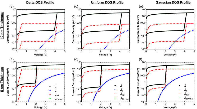
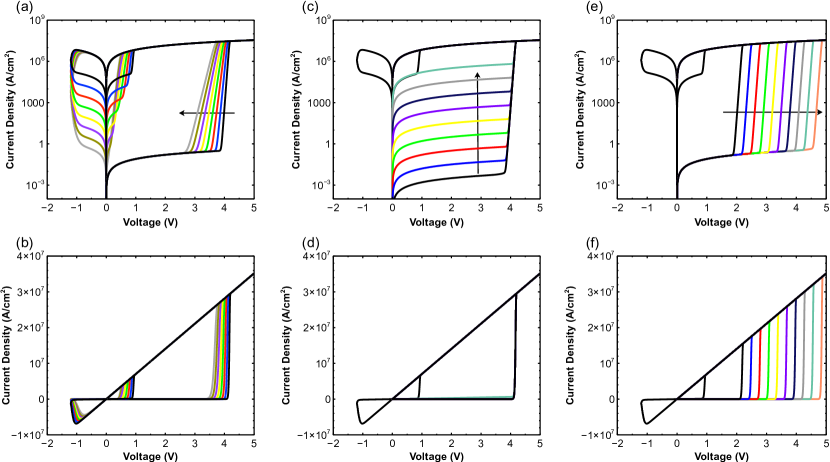
Figure 2 shows the current density versus voltage for the forming operation. Three different DOS profiles are compared, defined in terms of the ionization energies relative to the conduction band minimum : delta profile (situated at ), uniform profile (throughout bandgap) and Gaussian profile (mean = , standard deviation = ). Figures 2(a), (c) and (e) correspond to an oxide thickness of whereas Figures 2(b), (d) and (f) correspond to an oxide thickness of .
For larger oxide thicknesses (i.e., ), the Ohmic conduction model dominates the total current and is independent of the choice of DOS profile. This is expected, since tunneling current (band to band and trap-assisted) decreases exponentially with oxide thickness and bulk contributions become more dominant. Ohmic conduction, by contrast, is a local bulk component dependent upon the total defect concentration as opposed to the defect energy levels and/or their positions relative to the electrodes.
As the oxide thickness reduces (i.e., ), the importance of tunneling components increases, particularly during the transition from the pre-forming high-resistance state to post-forming low-resistance state. Furthermore, the voltage dependence of the trap-assisted tunneling current becomes increasingly linear as the DOS profile is broadened from a delta profile to that of a uniform and gaussian profile. This is to be expected, since for small voltages, the current is proportional to the emission rate of a single trap state (if a delta profile is assumed), which is exponentially dependent on voltage. A continuous DOS allows for emission from multiple states at a given voltage, broadening the current-voltage dependence computed using Equation 37. In our previous work, a tunneling current was only considered, which produced linear current-voltage characteristics due to the varied contribution of defects in terms of their position and/or energy level zeumault_tcad_2021 . We also note that the TAT current saturates for a single energy level (as seen in a Figures 2(a), (b)) when the applied voltage is large enough that the thermal barrier to emission becomes zero (or negative). Beyond this voltage, the emission rate is equal to the pre-exponential factor.
| (56) |
Importantly, these results suggest that, provided that the oxide thickness is not too small where tunneling significant occurs, the Ohmic conduction dominates the total current independent from the DOS profile. This allows a delta DOS profile to be used, which is more computationally efficient, despite being less representative of the physical reality as previously discussed. Importantly, setting the DOS profile as the delta profile,
| (57) |
removes the integrals from Equations 9 and 37.
| (58) |
| (59) |
Defining a net capture and emission rate , the rate equations can be succinctly and intuitively expressed.
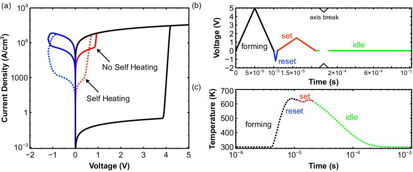
The expression for the empty states remains unchanged (Equation 11). Together, these represent a condensed, intuitive and more computatitonally efficient model that can represent the entirety of memristor characteristics as we show in Figure 3. Here, the model capability is compared with and without self-heating, showing forming, reset and set operations for a oxide thickness. Self heating has the effect of increasing the extent to which the device resets to a high-resistance state. The higher temperature during set shifts the set voltage towards lower values (Figure 3(c)). We have assumed that the entire forming, reset and set operations occur in sequence without delay (Figure 3(b)). If there is time between programming cycles (above ), the device will cool back to the ambient temperature (Figure 3(c)) during “idling” and the cumulative-effects of self-heating would be diminished. The time constant for recovery to the ambient temperature can be calculated from setting the Joule-heating term in in Equation 38 to zero, obtaining the familiar Newton’s cooling law result.
| (60) |
Using the parameter values in Table 1, . Assuming that the temperature has recovered within a total time equal to , the results shown in Figure 3(c) are sensible. The exact rate of recovery is expected to differ due to differences in memristor and electrode materials and device geometry.
In the following sections, we apply this delta-profile DOS model to gain an intuitive understanding of state variable dynamics, parameter dependencies and predictability, as well as making comparisons to experimental data.
III.1.2 State Variable Dynamics
In this section, we show how the state variables change with time. The essential aspects of the memristor model will be shown using the forming operation, to avoid restating similar trends that occurs from simply changing the polarity/magnitude of voltage. Importantly, during forming, the current exhibits a sharp increase from a low value to a high value at a certain voltage and the current-voltage characteristics exhibit hysteresis and a zero-crossing. In our model, an increase in current stems from an increase in oxygen vacancy concentration–through defect generation and electron capture. By contrast, a decrease in current stems from a decrease in vacancies–through recombination of unoccupied vacancies and electron emission from occupied vacancies.
Figure 4 shows the evolution of the state variables with time for DC and transient conditions for a forming operation from to . As shown in Figure 4(a),(b), the theoretical DC solution does not show hysteresis; the absence of hysteresis is evidenced by the fact that the state variables and current density are symmetric with respect to the applied voltage versus time waveform. This observation is common among physics-based memristor models, which has led to debates regarding whether these devices can, strictly speaking, be classified as memristors. However, as argued by Wang et al wang_well-posed_2016 , since the time scales needed to reach the theoretical DC solution are astronomically large, such arguments are not restrictive in practice and may be only of academic interest.
Furthermore, the lack of DC hysteresis suggests the low-resistance state of a memristor is metastable; the high-resistance state can be recovered by simply raising the device temperature. The DC current is negligible for small voltages because vacancies are unstable to recombination and/or electron emission in the infinite time (i.e., DC) or infinite temperature limit. This has been shown experimentally by Kumar et al kumar_Conduction_2016 –oxygen diffusion ultimately leading to recombination of Frenkel pairs at vacancy sites with full reset occuring over a time scale of minutes at temperatures of . In their work, the thermal barrier to recovery of the pre-forming high resistance state is , which is comparable to the thermal barrier to oxygen ion diffusion zeumault_tcad_2021 . Assuming an attempt frequency of , at a temperature of the time scale for diffusion would be which is much faster than the time scale observed for reset. Our model also considers electron emission as a parallel process whereby a conductive filament becomes more susceptible to dissolution (see Equation 9), since it has been shown that electron-occupied vacancies are more stable to recombination bradley_ElectronInjectionAssisted_2015 . Using nominal parameters, our model calculates an emission rate of to an assumed \ceTiN electrode from a trap with ionization energy of evaluated at low positive voltages . The time scale of this process is of the order of minutes and is more consistent with the experimental data in kumar_Conduction_2016 than a recombination process acting alone. It would be interesting to repeat this experiment for different electrode work functions to see if the thermal barrier is work function dependent and, therefore, if an electron-emission process has a rate-limiting effect on the recovery process.
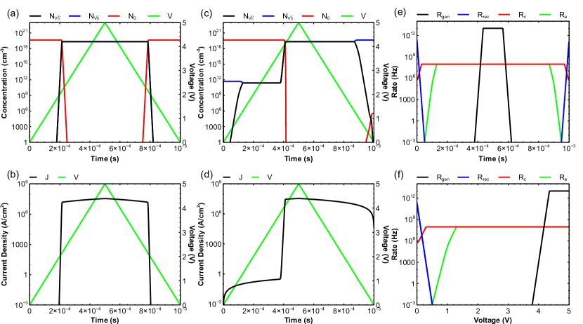
Transient simulations, by contrast, do show hysteresis. Ramped conditions favor electron capture as opposed to emission as a precursor for recombination, which is a comparatively much slower process for deep traps; electron capture forms a negatively charged vacancy which is more stable to recombination bradley_ElectronInjectionAssisted_2015 . This is shown in Figure 4 (c), (d) for a ramp rate of . This ramp rate is much slower, by many orders of magnitude, than ramp rates used during programming cycles in practice (e.g., write operations) which is of the order of . As shown in Figure 4(f), the emission rate remains lower than the capture rate (by many orders of magnitude) at low voltages until . At this voltage, the Fermi level of the top electrode is approximately aligned with the trap level at , increasing the emission rate to become comparable to the capture rate. When the capture and emission rates are both high–for positive voltages–the rate of recombination is low, preventing reset; for negative voltages the recombination rate is high, leading to reset. Eventually, the generation rate becomes substantial at large positive voltages, causing the vacancy concentration to increase. On the reverse sweep, the emission rate falls off, stabilizing a large concentration of occupied vacancies and a corresponding low resistance state. Thus, for all practical purposes, the model can be regarded as capable of reproducing hysteresis, and would accurately predict the vanishing of hysteresis at temperatures exceeding and for pulses exceeding minutes in duration.
In both cases (DC and transient), the transition from a pre-forming high resistance state to a post-forming low resistance state is coincident with a reduction in the concentration of empty states and corresponding increase in vacancies and . Qualitatively, this is similar in effect to a reduction in tunneling gap according to previous models guan_SPICE_2012 . On the forward sweep, due to the large difference in the rate of electronic processes and atomic processes, the increase in tracks the exponential increase in since electron capture is energetically favorable from the bottom electrode for positive applied voltage . On the reverse sweep, the concentration of occupied vacancies is stable due to a sizeable thermal barrier to emission; the barrier is stable since the trap level is lower than the Fermi energy of either a electrode (i.e., ). The new value of reached once the voltage at the top electrode returns to zero is based on a balance between the rate of recombination of Frenkel pairs and the combined rate of electron capture according to Equation 12. This can be seen from the increase in the concentration of empty states and a decrease in unoccupied vacancies towards the end of the pulse .
We note that a particular strength of our approach is that, based on Equation 1, the state variables are bound between the atomic density and zero, provided the rates are finite. As pointed out by Wang et al wang_well-posed_2016 , the use of a physical description based on a tunneling gap as a state variable requires the use of a window function to prevent the gap from diminishing below zero or extending beyond the oxide thickness. Using the oxygen vacancy concentrations as state variables eliminates the need for such a window function.
III.1.3 Predictive Capability of Model
Figure 5 shows the predictive capability of the model for variable temperature (a),(b), intitial vacancy concentration (c),(d) and activation enthalpy (e),(f). Pulse durations used were , and for forming, reset and set respectively.
Temperature was varied from to . Temperature changes affect the onset forming and set voltage and the resistance level following reset. At higher temperatures, the voltage required for forming is reduced; this indicates an increase in the rate of forming kinetics as predicted by the thermochemical model of dielectric breakdown mcpherson_thermochemical_2003 ; this has also been confirmed experimentally, by measuring the time required to form at various temperatures lorenzi_forming_2013 . Importantly, a higher temperature increases the rate of electron emission from occupied vacancies, creating more unoccupied vacancies which are available for recombination with oxygen ions, therefore increasing the rate of reset.
The initial vacancy concentration was varied from to . An increase in vacancy concentration has the effect of modifying the high-resistance state of the oxide film prior to forming only; as expected, a higher defect concentration leads to a higher current density and a lower resistance level; this parameter can be adjusted to reflect differences in preparation techniques used to deposit oxide thin films which will change due to processing parameters.
Lastly, the activation enthalpy of Frenkel pair generation is modified from to . As expected from Equation 16, the voltage required for forming linearly increases with an increase in activation enthalpy. Again, this follows from the thermochemical model of dielectric breakdown mcpherson_underlying_1998 ; mcpherson_thermochemical_2003 ; this parameter can be adjusted to match forming voltages extracted from experimental data sets. To match set voltages, a separate activation enthalpy is used (not shown).
In the next section, we illustrate choice of these parameters using an experimental dataset.
III.2 Model Validation and Testing
III.2.1 Comparison to Experimental Data
Having demonstrated the general behavior of the model, we now utilize this framework to develop a circuit-compatible compact model in Verilog-A based upon a delta DOS profile.
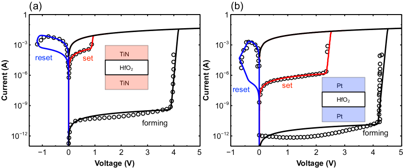
First, we compare our compact model (using delta DOS profile) with two different \ceHfO2-based memristors having different electrode materials in which the \ceHfO2 layer was identically processed using atomic layer deposition at lorenzi_forming_2013 . This dataset was selected based on the availability of processing and characterization data which provides details regarding the structure of the \ceHfO2 layer in addition to the electrode interfaces cabout_Role_2013 ; jorel_Physicochemical_2009a ; lorenzi_forming_2013 . The memristors have identical geometry (area = , oxide thickness = ) with an electrode thickness of . The devices have symmetric electrode configurations \ceTiN/\ceHfO2/\ceTiN (shown in Figure 6(a)) and \cePt/\ceHfO2/\cePt (shown in Figure 6(b)). Apart from an apparent negative differential resistance in the as-prepared (pre-forming) state present in both but particularly pronounced in the \cePt/\ceHfO2/\cePt device (likely due to initial charging of interface traps rofan_Stressinduced_1991 ; chen_Reliability_ ), the devices are well-behaved. We note that other devices prepared using the same process show similar forming voltages and reduced current magnitudes without NDR behavior cagli_Experimental_2011 and are therefore within the large statistical spread of these devices lorenzi_forming_2013 and qualitatively identical. Electrode parameters were used from prior literature reports for \ceTiN lima_Titanium_2012 ; solovan_Electrical_2014 ; walker_estimate_1998 and \cePt schaeffer_Contributions_2004 ; fischer_Mean_1980 ; hoffmann_Electrical_1976 thin-films.
The simulated current-voltage characteristics for these two \ceHfO2 memristors are compared with experimental data reported in lorenzi_forming_2013 in Figure 6 (a) and (b). As evidenced by the smaller current in the pre-forming state, the \cePt electrode device is fit using a smaller initial oxygen vacancy concentration. The authors report a higher oxygen vacancy concentration in \ceHfO2 films fabricated on \ceTiN (and \ceTi) as opposed to films grown on \cePt, attributed to the formation of a titania suboxide (\ceTiO_x) interfacial layer. This is sensible from a thermodynamics perspective given the large formation enthalpy of \ceTiO2 and the associated gettering behavior of \ceTi stout_Gettering_1955 . Importantly, from a modeling perspective, this justifies the increase in the initial oxygen vacancy concentration in \ceHfO2 films deposited on \ceTiN.
The forming and set voltages are higher for the \cePt electrode device than the \ceTiN electrode device. The authors attribute the reduction in forming voltage to a reduced formation enthalpy of Frenkel pairs within the vacancy-rich interfacial layer adjacent to the \ceTiN electrodes. The lower formation enthalpy may reflect the fact that nearest-neighbor pairs and clusters of oxygen vacancies are more stable than point defects bradley_ElectronInjectionAssisted_2015 ; vacancy clusters ultimately produce what is regarded as a “conductive filament" and are present after initial forming. For the forming data shown in Figure 6(a), the forming voltage is on the higher end of the statistical variation reported for \ceTi/\ceTiN based electrodes, which can be much lower by a couple volts cabout_Role_2013 . Although this explanation is consistent with theoretical investigations in the formation of vacancy clusters, it should be noted that the formation of positive space charge (e.g., unoccupied oxygen vacancies) near the anode/TE or negative space charge (e.g., negative oxygen vacancies) near the cathode/BE would be expected to lead to a local field enhancement within the oxide–both reducing the forming voltage. Additionally, the stoichiometric changes (when corrected for improvements to polarizability due to crystallization venkataiah_Oxygen_2021 ) can possibly lead to changes in forming and set voltages according to the thermochemical model (Equation 16).
| (61) |
Thus, either a reduction in formation enthalpy or an increase in polarization (e.g., relative permittivity or molecular dipole moment) could be used to describe the differences in transition voltages in these datasets. Here, to describe the forming/set operations, the activation energy for Frenkel pair generation was reduced. We note that the transition voltages are sweep rate dependent; we have used linear voltage ramps over the indicated voltage ranges with a total time interval per segment of for forming and set and for reset operations in both devices corresponding to ramp rates between and , consistent with the reports for this dataset cabout_Role_2013 .
The authors also report the presence of different crystalline phases between the two \ceHfO2 films – films grown on \ceTi or \ceTiN are predominantly orthorhombic whereas films grown on \cePt are predominantly monoclinic. The monoclinic phase is the least polarizable among the polymorphs of \ceHfO2 with a relative permmitivity of 18 and 29 for the cubic phase zhao_Firstprinciples_2002 . The dominant orthorhombic phase observed on \ceTiN is therefore consistent with a reduced forming/set voltage relative to monoclinic films grown on \cePt without need for reducing the activation enthalpy. The oxygen vacancy formation energy in both phases is similar at the same Fermi level position wei_Intrinsic_2021 , so the ionization energy is kept the same when fitting the datasets. Only a slight increase in capture cross section (from to ) was needed to fit the \cePt devices.
In sum, for both datasets, our compact model demonstrates a close match with the experiments in all operating conditions (forming, set, and reset) of a memristor. The many physical considerations emphasize the need for detailed characterization in order to leverage the model’s predictive capability and justify changes to particular parameters over others. Table 2 lists the parameter values adjusted to achieve good agreement between the modeled and measured data.
| [] | [] | [] | [] | [] | [] | |
|---|---|---|---|---|---|---|
| \ceTiN/\ceHfO2/\ceTiN | ||||||
| \cePt/\ceHfO2/\cePt |
III.2.2 Simulation of 4x4 1T1R Nonvolatile Memory Array
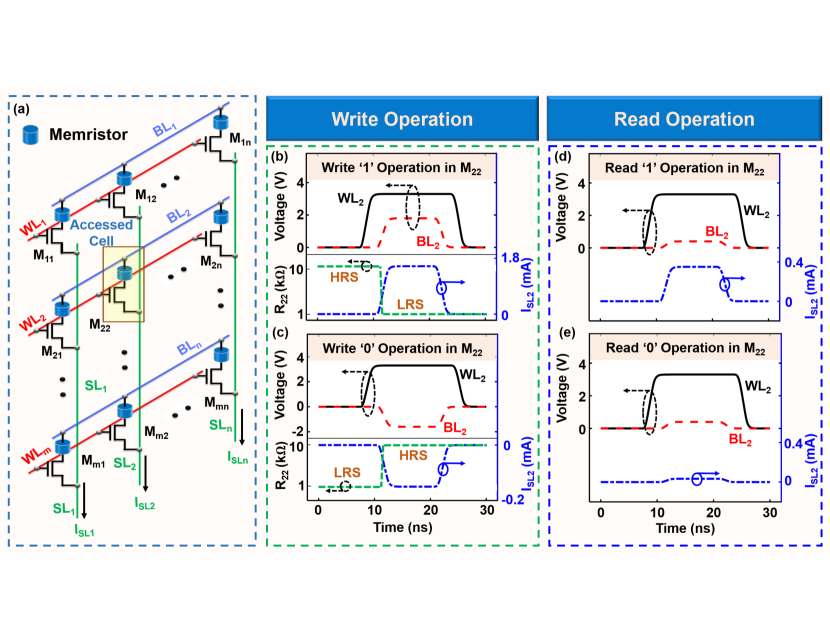
Finally, to demonstrate the usability of our model and prove that our model can be self-consistently coupled with other circuit elements, we simulate a 1-transistor 1-memristor (1T1R) array (shown in Fig. 7(a)). In our simulation, we use the DGXFET models available in the IBM CMOS 10LPe process for the access transistors and our compact model calibrated with the experiment Aziza2019 for the memristor-based memory elements. In memristor-based memory systems, two resistance levels – HRS (high resistance state) and LRS(low resistance state) – are used to define the memory states (logic ’0’ and logic ’1’, respectively). Here, we demonstrate the write and read operations in the (2, 2) cell of the array. To access the cell, we fist apply the suitable voltage to the corresponding WL to turn the access transistor ON (see top panels of Figs. 7(b), (c), (d), and (e)). Then, to write into (read from) the accessed cell, we apply the suitable write voltage (read voltage) to the BL . The remaining WLs and BLs are kept at ground.
Figures 7(b) and (c) show that with the suitable biases at WLs and BLs, the resistance of the accessed cell switches from one state to another: HRS LRS during write ’1’ and LRS HRS during write ’0’ operations. During the read operation, for a same amount of voltage at the BL, we observe two levels of current based on the stored memory state in the cell–high current for logic ’1’ and low current for logic ’0’ states. A simple current sense amplifier Chang2013 ; aziz_Low_2017 with a suitable reference can be used for the sensing purpose thanks to the distinct current levels corresponding to two memory states.
IV Conclusions
In summary, a new compact model for oxide memristors was presented, based on the use of oxygen vacancy concentration as state variable. The theoretical model is based upon a recent manuscript which combined rates of atomic processes (e.g., Frenkel pair generation and recombination, diffusion of point defects) with those of electronic processes (electron capture and emission), in a kinetic Monte Carlo simulation approach. The compact model was validated using bulk parameters for \ceHfO2, though is of general utility to a wide range of single phase, insulating oxides or polymorphs which can be described using “effective” bulk-averaged parameters. The dynamic evolution of the state variables – the concentrations of occupied and unoccupied oxygen vacancies – was shown to be capable, both qualitatively and quantitatively, of reproducing the essential switching characteristics of oxide memristors. In particular, the increase (decrease) in oxygen vacancy concentration is qualitatively similar in effect to the more familiar reduction (expansion) of the tunnel gap which has been used in existing compact models. Key strengths of this approach include: the state variables are bound between zero and the atomic density of the oxide without the use of a window function – needed for preventing tunnel gaps from becoming negative or exceeding the oxide thickness; the model makes few assumptions regarding the “filament" geometry, being chiefly based upon the number density of oxygen vacancy defects as opposed to their geometry; the model provides an intuitive description of resistive switching that is consistent with retention improvements observed in lower work-function metal electrodes (e.g., \ceTi/\ceTiN) compared to \cePt due to an increased emission barrier which stabilizes the low-resistance state; the model can be easily refined via inclusion of image force correction or Poole-Frenkel modeling of high-resistance states without loss of generality.
As a test of its practical utility, the compact model was implemented in Verilog-A, verified using well-defined experimental data-sets with different electrode geometries, and tested in circuit simulation using a 4x4 one-transistor, one-resistor (1T1R) memory cells, representative of a small, nonvolatile memory array. We anticipate that this model will serve as an alternate description of memristor switching in terms of the concentration of defects as opposed to the state of the filament. Such a description will be particularly useful as new and ongoing experimental data emerges to suggest new or confirm existing geometrical descriptions of conductive filament shapes.
Data Availability Statement
The data that support the findings of this study are available from the corresponding author upon reasonable request.
References
- (1) M. P. Raj and G. Kavithaa, “Memristor based high speed and low power consumption memory design using deep search method,” J Ambient Intell Hum. Comput, vol. 12, pp. 4223–4235, 2021.
- (2) N. Du, H. Schmidt, and I. Polian, “Low-power emerging memristive designs towards secure hardware systems for applications in internet of things,” Nano Materials Science, vol. 3-2, pp. 186–204, 2021.
- (3) G. Sun, Y. Joo, Y. Chen, D. Niu, Y. Xie, Y. Chen, and H. Li, “A hybrid solid-state storage architecture for the performance, energy consumption, and lifetime improvement,” HPCA - 16 2010 Sixt. Int. Symp. High-Perform. Comput. Archit., vol. 11246505, Sept. 2010.
- (4) A. Thomas, “Memristor-based neural networks,” J. Phys. D, Appl. Phys., vol. 46-9, p. 093001, 2013.
- (5) Q. Lu, F. Sun, L. Liu, L. Li, Y. Wang, M. Hao, Z. Wang, S. Wang, and T. Zhang, “Biological receptor-inspired flexible artificial synapse based on ionic dynamics,” Microsyst. Nanoeng., vol. 6, p. 84, 2020.
- (6) L. Chen, C. Li, T. Huang, Y. Chen, S. Wen, and J. Qi, “A synapse memristor model with forgetting effect,” Phys. Lett. A, vol. 377, pp. 3260–3265, 2013.
- (7) Y. Zhang, X. Wang, Y. Li, and E. G. Friedman, “Memristive model for synaptic circuits,” IEEE Trans. Circuits Syst. II, vol. 64, pp. 767–771, 2017.
- (8) I. Vourkas, A. Batsos, and G. C. Sirakoulis, “SPICE modeling of nonlinear memristive behavior,” Int. J. Circuit Theory Appl., vol. 43, pp. 553–565, 2015.
- (9) X. Guan, S. Yu, and H.-S. P. Wong, “A SPICE Compact Model of Metal Oxide Resistive Switching Memory With Variations,” IEEE Electron Device Lett., vol. 33, pp. 1405–1407, Oct. 2012.
- (10) P.-Y. Chen and S. Yu, “Compact Modeling of RRAM Devices and Its Applications in 1T1R and 1S1R Array Design,” IEEE Trans. Electron Devices, vol. 62(12), pp. 4022–4028, 2015.
- (11) M. Bocquet, D. Deleruyelle, H. Aziza, C. Muller, J.-M. Portal, T. Cabout, and E. Jalaguier, “Robust compact model for bipolar oxide-based resistive switching memories,” IEEE Trans. Electron Devices, vol. 61, pp. 674–681, 2014.
- (12) D. Biolek, V. Biolkova, and Z. Biolek, “SPICE model of memristor with nonlinear dopant drift,” Radioengineering, vol. 18, pp. 210–214, 2009.
- (13) S. Kvatinsky, E. G. Friedman, A. Kolodny, and U. C. Weiser, “TEAM: Threshold adaptive memristor model,” IEEE Trans. Circuits Syst. I, vol. 60, pp. 211–221, 2013.
- (14) B. Gao, S. Yu, N. Xu, L. F. Liu, B. Sun, X. Y. Liu, R. Q. Han, J. F. Kang, B. Yu, and Y. Wang, “Oxide-based RRAM switching mechanism: A new ion-transport recombination model,” Proc. IEEE IEDM, pp. 1–4, 2008.
- (15) S. Larentis, F. Nardi, S. Balatti, D. C. Gilmer, and D. Ielmini, “Resistive switching by voltage-driven ion migration in bipolar RRAM—Part II: Modeling,” IEEE Trans. Electron Devices, vol. 59, pp. 2468–2475, 2012.
- (16) D. C. Gilmer, G. Bersuker, S. Koveshnikov, M. Jo, A. Kalantarian, B. Butcher, R. Geer, Y. Nishi, P. D. Kirsch, and R. Jammy, “Asymmetry, vacancy engineering and mechanism for bipolar RRAM,” Proc IEEE Int Mem. Workshop, pp. 1–4, 2012.
- (17) L. Vandelli, A. Padovani, L. Larcher, G. Bersuker, D. Gilmer, and P. Pavan, “Modeling of forming operation in HfO2-based resistive switching memories,” Proc IEEE Int Mem. Workshop, 2011.
- (18) F. Nardi, S. Larentis, S. Balatti, D. C. Gilmer, and D. Ielmini, “Resistive switching by voltage-driven ion migration in bipolar RRAM—Part I: Experimental study,” IEEE Trans. Electron Devices, vol. 59, pp. 2461–2467, 2012.
- (19) P. Huang, X. Y. Liu, B. Chen, H. T. Li, Y. J. Wang, Y. X. Deng, K. L. Wei, L. Zeng, B. Gao, G. Du, X. Zhang, and J. F. Kang, “A physics-based compact model of metal-oxide-based RRAM DC and AC operations,” IEEE Trans. Electron Devices, vol. 60, no. 12, pp. 4090–4097, 2013.
- (20) J. Suñé, “New physics-based analytic approach to the thin-oxide breakdown statistics,” IEEE Electron Device Lett., vol. 22, pp. 294–296, 2001.
- (21) J. Suñé, S. Tous, and E. Y. Wu, “Analytical cell-based model for the breakdown statistics of multilayer insulator stacks,” IEEE Electron Device Lett., vol. 30, pp. 41359–1361, 2009.
- (22) S. Tous, E. Y. Wu, and J. Suñé, “A compact analytic model for the breakdown distribution of gate stack dielectrics,” Proc Int. Reliab. Phys. Symp., pp. 792–798, 2010.
- (23) S. Long, X. Lian, C. Cagli, L. Perniola, E. Miranda, D. Jiménez, H. Lv, Q. Liu, L. Li, Z. Huo, M. Liu, and J. Suñé, “Compact analytical models for the SET and RESET switching statistics of RRAM inspired in the cell-based percolation model of gate dielectric breakdown,” Proc IEEE Int Rel Phys Symp IRPS, pp. 5A.6.1–5A.6.8, 2013.
- (24) S. Kumar, Z. Wang, X. Huang, N. Kumari, N. Davila, J. P. Strachan, D. Vine, A. L. D. Kilcoyne, Y. Nishi, and R. S. Williams, “Conduction Channel Formation and Dissolution Due to Oxygen Thermophoresis/Diffusion in Hafnium Oxide Memristors,” ACS Nano, vol. 10, pp. 11205–11210, Dec. 2016.
- (25) A. Alexandrov, A. Bratkovsky, B. Bridle, S. Savel’ev, D. Strukov, and R. S. Williams, “Current-controlled negative differential resistance due to Joule heating in TiO,” Appl. Phys. Lett., vol. 99, p. 202104, 2011.
- (26) S. M. Sze and K. K. Ng, Physics of Semiconductor Devices. John Wiley & Sons, Dec. 2006.
- (27) S. Yu and H.-S. P. Wong, “A Phenomenological Model for the Reset Mechanism of Metal Oxide RRAM,” IEEE Electron Device Lett., vol. 31, pp. 1455–1457, Dec. 2010.
- (28) S. Aldana, P. Garcia-Fernandez, R. Romero-Zaliz, M. B. Gonzalez, F. Jimenez-Molinos, F. Gomez-Campos, F. Campabadal, and J. B. Roldan, “Resistive switching in HfO2 based valence change memories, a comprehensive 3D kinetic Monte Carlo approach,” J. Phys. -Appl. Phys., vol. 53, May 2020.
- (29) X. Xu, B. Rajendran, and M. P. Anantram, “Kinetic Monte Carlo Simulation of Interface-Controlled Hafnia-Based Resistive Memory,” IEEE Trans. Electron Devices, vol. 67, pp. 118–124, Jan. 2020.
- (30) Z. Jiang, S. Yu, Y. Wu, J. H. Engel, X. Guan, and H.-S. P. Wong, “Verilog A Compact Model for Oxide-Based Resistive Random Access Memory (RRAM),” Int. Conf. Simul. Semicond. Process. Devices SISPADIEEE, pp. 41–44, 2014.
- (31) X. Guan, S. Yu, and H.-S. P. Wong, “On the Switching Parameter Variation of Metal-Oxide RRAM—Part I: Physical Modeling and Simulation Methodology,” IEEE Trans. Electron Devices, vol. 59, pp. 1172–1182, Apr. 2012.
- (32) L. Chua, “Memristor-the missing circuit element,” IEEE Trans. Circuit Theory, vol. 18, pp. 507–519, 1971.
- (33) S. Amer, S. Sayyaparaju, G. S. Rose, K. Beckmann, and N. C. Cady, “A Practical Hafnium-Oxide Memristor Model Suitable for Circuit Design and Simulation,” IEEE Int. Symp. Circuits Syst. ISCAS, 2017.
- (34) M. D. Pickett, D. B. Strukov, J. L. Borghetti, J. J. Yang, G. S. Snider, D. R. Stewart, and R. S. Williams, “Switching dynamics in titanium dioxide memristive devices,” Journal of Applied Physics, vol. 106, p. 074508, Oct. 2009.
- (35) S. R. Bradley, A. L. Shluger, and G. Bersuker, “Electron-Injection-Assisted Generation of Oxygen Vacancies in Monoclinic HfO 2,” Phys. Rev. Applied, vol. 4, p. 064008, Dec. 2015.
- (36) S. Aldana, P. García-Fernández, A. Rodríguez-Fernández, R. Romero-Zaliz, M. B. González, F. Jiménez-Molinos, F. Campabadal, F. Gómez-Campos, and J. B. Roldán, “A 3D kinetic Monte Carlo simulation study of resistive switching processes in Ni/HfO 2 /Si-n + -based RRAMs,” J. Phys. D: Appl. Phys., vol. 50, p. 335103, Aug. 2017.
- (37) A. Zeumault, S. Alam, Z. Wood, R. J. Weiss, A. Aziz, and G. S. Rose, “TCAD Modeling of Resistive-Switching of HfO2 Memristors: Efficient Device-Circuit Co-Design for Neuromorphic Systems,” Front. Nanotechnol., vol. 3, 2021.
- (38) C. Li, B. Gao, Y. Yao, X. Guan, X. Shen, Y. Wang, P. Huang, L. Liu, X. Liu, J. Li, C. Gu, J. Kang, and R. Yu, “Direct Observations of Nanofilament Evolution in Switching Processes in HfO 2 -Based Resistive Random Access Memory by In Situ TEM Studies,” Adv. Mater., vol. 29, p. 1602976, Mar. 2017.
- (39) R. Thamankar, N. Raghavan, J. Molina, F. M. Puglisi, S. J. O’Shea, K. Shubhakar, L. Larcher, P. Pavan, A. Padovani, and K. L. Pey, “Single vacancy defect spectroscopy on HfO 2 using random telegraph noise signals from scanning tunneling microscopy,” Journal of Applied Physics, vol. 119, p. 084304, Feb. 2016.
- (40) J. McPherson, J.-Y. Kim, A. Shanware, and H. Mogul, “Thermochemical description of dielectric breakdown in high dielectric constant materials,” Appl. Phys. Lett., vol. 82, pp. 2121–2123, Mar. 2003.
- (41) J. W. McPherson and H. C. Mogul, “Underlying physics of the thermochemical E model in describing low-field time-dependent dielectric breakdown in SiO2 thin films,” Journal of Applied Physics, vol. 84, pp. 1513–1523, Aug. 1998.
- (42) F. Jiménez-Molinos, F. Gámiz, A. Palma, P. Cartujo, and J. A. López-Villanueva, “Direct and trap-assisted elastic tunneling through ultrathin gate oxides,” Journal of Applied Physics, vol. 91, pp. 5116–5124, Apr. 2002.
- (43) A. Palma, A. Godoy, J. A. Jiménez-Tejada, J. E. Carceller, and J. A. López-Villanueva, “Quantum two-dimensional calculation of time constants of random telegraph signals in metal-oxide–semiconductor structures,” Phys. Rev. B, vol. 56, pp. 9565–9574, Oct. 1997.
- (44) Synopsys, “TCAD Sentaurus,” Online, 2019.
- (45) S. Aldana, P. Garcia-Fernandez, R. Romero-Zaliz, M. B. Gonzalez, F. Jimenez-Molinos, F. Campabadal, F. Gomez-Campos, and J. B. Roldan, “A kinetic Monte Carlo simulator to characterize resistive switching and charge conduction in Ni/HfO2/Si RRAMs,” in PROCEEDINGS OF THE 2018 12TH SPANISH CONFERENCE ON ELECTRON DEVICES (CDE) (Mateos, J and Gonzalez, T, ed.), Spanish Conference on Electron Devices, (NEW YORK, NY 10017 USA), IEEE, 2018.
- (46) L. Larcher, A. Padovani, O. Pirrotta, L. Vandelli, and G. Bersuker, “Microscopic understanding and modeling of HfO2 RRAM device physics,” in 2012 International Electron Devices Meeting, pp. 20.1.1–20.1.4, Dec. 2012.
- (47) J. G. Simmons, “Generalized Formula for the Electric Tunnel Effect between Similar Electrodes Separated by a Thin Insulating Film,” J. Appl. Phys., vol. 34, pp. 1793–1803, June 1963.
- (48) A. Schenk, Advanced Physical Models for Silicon Device Simulation. Springer Science & Business Media, July 1998.
- (49) L. Zhang, Y.-Y. Hsu, F. T. Chen, H.-Y. Lee, Y.-S. Chen, W.-S. Chen, P.-Y. Gu, W.-H. Liu, S.-M. Wang, C.-H. Tsai, R. Huang, and M.-J. Tsai, “Experimental investigation of the reliability issue of RRAM based on high resistance state conduction,” Nanotechnology, vol. 22, p. 254016, June 2011.
- (50) M. A. Panzer, M. Shandalov, J. A. Rowlette, Y. Oshima, Y. W. Chen, P. C. McIntyre, and K. E. Goodson, “Thermal Properties of Ultrathin Hafnium Oxide Gate Dielectric Films,” IEEE Electron Device Lett., vol. 30, pp. 1269–1271, Dec. 2009.
- (51) T. Wang and J. Roychowdhury, “Well-Posed Models of Memristive Devices,” arXiv:1605.04897, 2016.
- (52) P. Lorenzi, R. Rao, and F. Irrera, “Forming Kinetics in HfO2-Based RRAM Cells,” IEEE Trans. Electron Devices, vol. 60, pp. 438–443, Jan. 2013.
- (53) T. Cabout, J. Buckley, C. Cagli, V. Jousseaume, J. F. Nodin, B. de Salvo, M. Bocquet, and C. Muller, “Role of Ti and Pt electrodes on resistance switching variability of HfO2-based Resistive Random Access Memory,” Thin Solid Films, vol. 533, pp. 19–23, Apr. 2013.
- (54) C. Jorel, C. Vallée, E. Gourvest, B. Pelissier, M. Kahn, M. Bonvalot, and P. Gonon, “Physicochemical and electrical characterizations of atomic layer deposition grown HfO[sub 2] on TiN and Pt for metal-insulator-metal application,” J. Vac. Sci. Technol. B, vol. 27, no. 1, p. 378, 2009.
- (55) R. Rofan and C. Hu, “Stress-induced oxide leakage,” IEEE Electron Device Lett., vol. 12, pp. 632–634, Nov. 1991.
- (56) Y. Chen, Reliability Characterizations of Ultra-Thin Gate Oxides of MOSFETs. PhD thesis, University of Maryland, College Park, United States – Maryland.
- (57) C. Cagli, J. Buckley, V. Jousseaume, T. Cabout, A. Salaun, H. Grampeix, J. F. Nodin, H. Feldis, A. Persico, J. Cluzel, P. Lorenzi, L. Massari, R. Rao, F. Irrera, F. Aussenac, C. Carabasse, M. Coue, P. Calka, E. Martinez, L. Perniola, P. Blaise, Z. Fang, Y. H. Yu, G. Ghibaudo, D. Deleruyelle, M. Bocquet, C. Müller, A. Padovani, O. Pirrotta, L. Vandelli, L. Larcher, G. Reimbold, and B. de Salvo, “Experimental and theoretical study of electrode effects in HfO2 based RRAM,” in 2011 International Electron Devices Meeting, pp. 28.7.1–28.7.4, Dec. 2011.
- (58) L. Lima, J. Diniz, I. Doi, and J. Godoy Fo, “Titanium nitride as electrode for MOS technology and Schottky diode: Alternative extraction method of titanium nitride work function,” Microelectronic Engineering, vol. 92, pp. 86–90, Apr. 2012.
- (59) M. N. Solovan, V. V. Brus, E. V. Maistruk, and P. D. Maryanchuk, “Electrical and optical properties of TiN thin films,” Inorg Mater, vol. 50, pp. 40–45, Jan. 2014.
- (60) C. G. H. Walker, J. A. D. Matthew, C. A. Anderson, and N. M. D. Brown, “An estimate of the electron effective mass in titanium nitride using UPS and EELS,” Surface Science, vol. 412–413, pp. 405–414, Sept. 1998.
- (61) J. K. Schaeffer, L. R. C. Fonseca, S. B. Samavedam, Y. Liang, P. J. Tobin, and B. E. White, “Contributions to the effective work function of platinum on hafnium dioxide,” Appl. Phys. Lett., vol. 85, pp. 1826–1828, Sept. 2004.
- (62) G. Fischer, H. Hoffmann, and J. Vancea, “Mean free path and density of conductance electrons in platinum determined by the size effect in extremely thin films,” Phys. Rev. B, vol. 22, pp. 6065–6073, Dec. 1980.
- (63) H. Hoffmann and G. Fischer, “Electrical conductivity in thin and very thin platinum films,” Thin Solid Films, vol. 36, pp. 25–28, July 1976.
- (64) V. L. Stout and M. D. Gibbons, “Gettering of Gas by Titanium,” J. Appl. Phys., vol. 26, pp. 1488–1492, Dec. 1955.
- (65) S. Venkataiah, S. J. Chandra, U. Chalapathi, C. Ramana, and S. Uthanna, “Oxygen partial pressure influenced stoichiometry, structural, electrical, and optical properties of DC reactive sputtered hafnium oxide films,” Surf. Interface Anal., vol. 53, no. 2, pp. 206–214, 2021.
- (66) X. Zhao and D. Vanderbilt, “First-principles study of structural, vibrational, and lattice dielectric properties of hafnium oxide,” Phys. Rev. B, vol. 65, p. 233106, June 2002.
- (67) J. Wei, L. Jiang, M. Huang, Y. Wu, and S. Chen, “Intrinsic Defect Limit to the Growth of Orthorhombic HfO2 and (Hf,Zr)O2 with Strong Ferroelectricity: First-Principles Insights,” Adv. Funct. Mater., vol. 31, no. 42, p. 2104913, 2021.
- (68) H. Aziza, H. Bazzi, J. Postel-Pellerin, P. Canet, M. Moreau, and A. Harb, “An augmented OxRAM synapse for spiking neural network (SNN) Circuits,” Proceedings - 2019 14th IEEE International Conference on Design and Technology of Integrated Systems In Nanoscale Era, DTIS 2019, apr 2019.
- (69) M. F. Chang, S. J. Shen, C. C. Liu, C. W. Wu, Y. F. Lin, Y. C. King, C. J. Lin, H. J. Liao, Y. D. Chih, and H. Yamauchi, “An offset-tolerant fast-random-read current-sampling-based sense amplifier for small-cell-current nonvolatile memory,” IEEE Journal of Solid-State Circuits, vol. 48, no. 3, pp. 864–877, 2013.
- (70) A. Aziz, X. Li, N. Shukla, S. Datta, M.-F. Chang, V. Narayanan, and S. K. Gupta, “Low power current sense amplifier based on phase transition material,” in 2017 75th Annual Device Research Conference (DRC), pp. 1–2, June 2017.