A 120dB Programmable-Range On-Chip Pulse Generator for Characterizing Ferroelectric Devices ††thanks: This work received funding from the European Union’s H2020 research and innovation programme under the H2020 BeFerrosynaptic (871737), MeM-Scales (871371) projects.
Abstract
Novel non-volatile memory devices based on ferroelectric thin films represent a promising emerging technology that is ideally suited for neuromorphic applications. The physical switching mechanism in such films is the nucleation and growth of ferroelectric domains. Since this has a strong dependence on both pulse width and voltage amplitude, it is important to use precise pulsing schemes for a thorough characterization of their behavior. In this work, we present an on-chip 120 dB programmable range pulse generator, that can generate pulse widths ranging from 10 ns to 10 ms 2.5% which eliminates the RLC bottleneck in the device characterisation setup. We describe the pulse generator design and show how the pulse width can be tuned with high accuracy, using Digital to Analog converters. Finally, we present experimental results measured from the circuit, fabricated using a standard 180 nm CMOS technology.
Index Terms:
Pulse Generator, FTJ, FeFET, DAC, memory characterizationI Introduction
Thanks to their ultra-low power operation, Complementary Metal-Oxide-Semiconductor (CMOS)-compatibility, and non-volatility, ferroelectric hafnium oxide-based devices such as ferroelectric capacitors (FeCAP) [1], ferroelectric field effect transistors (FeFET) [2], and ferroelectric tunneling junctions (FTJ) [3] are widely explored for digital storage conventional memory array architectures [1, 2] as well as in novel bio-inspired architectures [4]. Besides multi-bit storage in digital memories, the analog switching properties of these nano-scale devices are important for the realization of synaptic weight elements [5, 6] or artificial neurons [7] for adoption in neuromorphic applications [8]. In order to allow proper device optimization and defining the constraints for circuit design, a profound understanding of the switching kinetics in such nano-scale devices is needed [9].
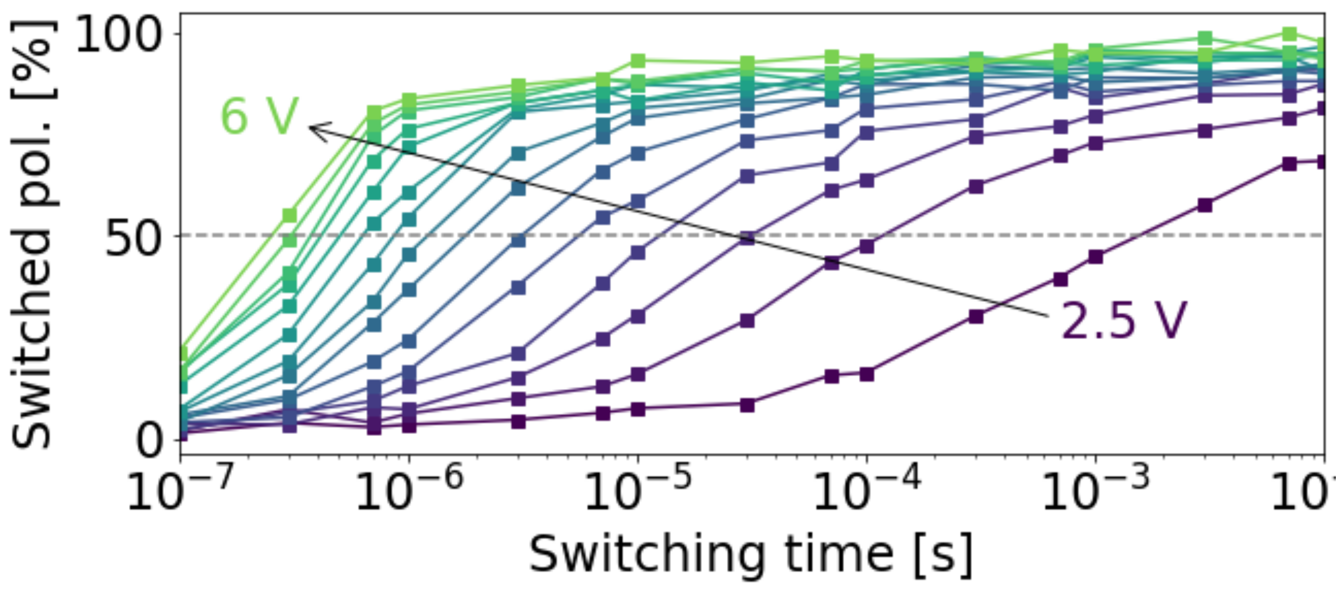
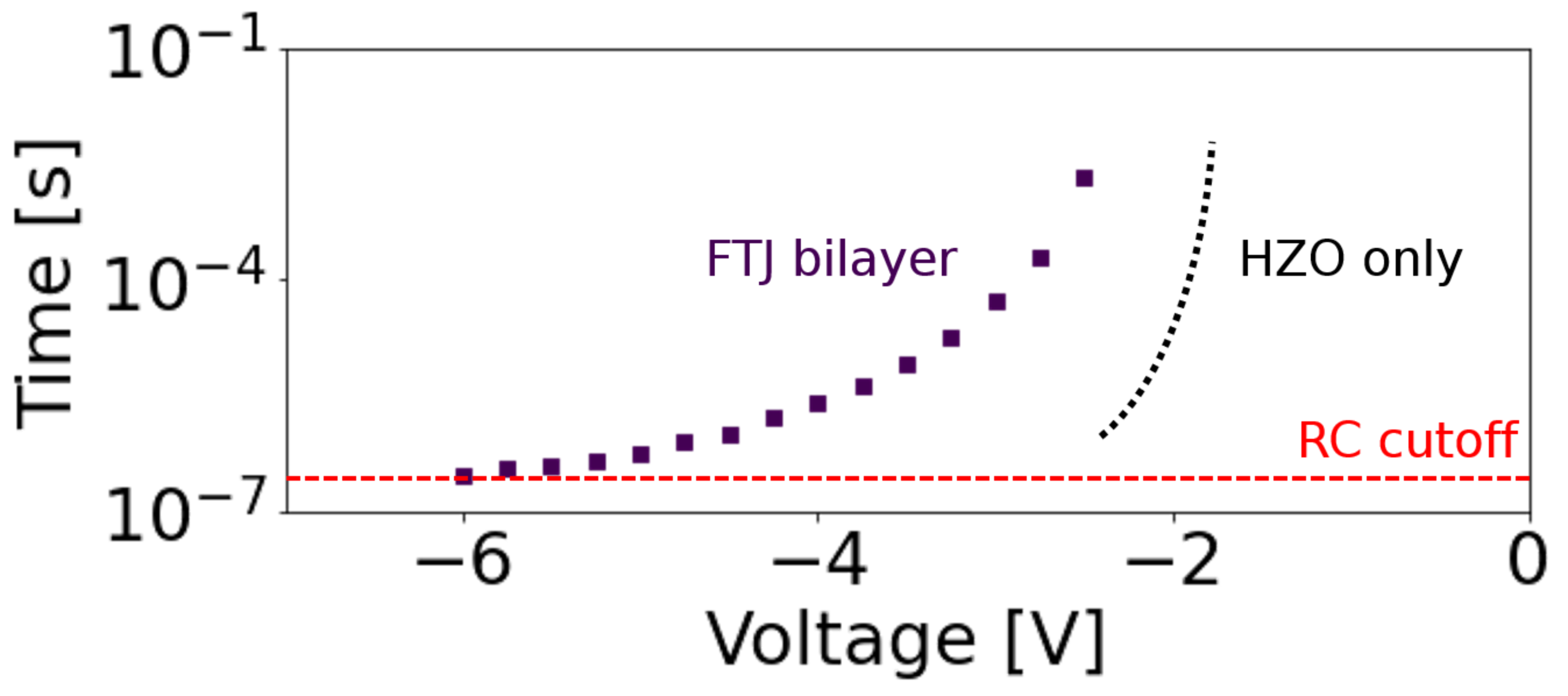
Figure 1(a) depicts the results of such a switching kinetics measurement for a bilayer FTJ device featuring a 10 nm ferroelectric hafnium-zirconium-oxide (HZO) and a 2 nm alumnium oxide (Al2O3) layer sandwiched between two titanium nitride (TiN) electrodes [3]. The diagram depicts the portion of switched polarization upon application of different switching pulses. Extracting the respective switching voltage and time at switched polarization results in the switching kinetics curve depicted in Fig. 1(b). Extrapolation of this data yields both the data retention time of the respective device [11] as well as the required pulse voltages for ns-switching times. The switching kinetics of a given device will be material- and size-dependent [9], and as such, the characterization should be performed on individual devices. As an example, when looking at the voltage-time dependence in Fig. 1(b) and comparing to the data for an HZO-only sample (extracted from [10]), there is a shift to larger voltages due to the voltage drop over the Al2O3 layer, and an asymptotic saturation of switching time between 100 ns and 1 s. This saturation is related to a RC-delay within the FTJ samples and measurement set-up that cannot be easily avoided. Similar issues occur for FeFET and FeCAP single devices, even though switching times down to just 14 ns to 20 ns have been demonstrated in integrated memory arrays [1, 2]. Obviously, the RC-delay has a strong impact on the extrapolation of switching kinetics, especially at shorter time scales, and consequently a pulse generator is required which is able to perform such a thorough characterization by applying pulses with varying amplitudes and timewidths directly on-chip. Moreover, for the characterization of multi-bit and analogue storage a very precise control of the switching pulses is mandatory [12], especially for the steep switching gradients at shorter pulse times (see Fig. 1(a)). In order to tackle this issue, we developed an optimized on-chip pulse-generator circuit, enabling the application of well-controlled voltage pulses with timings that span over six orders of magnitude.
II System Architecture
Figure 2 shows the architecture of the wide-range programmable on-chip pulse generator. On the arrival of the input pulses (shown as ), the programmable capacitor is abruptly charged to , and once the pulse is removed, it slowly discharges through the current. This results in a ramp voltage on node which when compared to a reference voltage (), generates a pulse at the output (). The slope of the ramp voltage is determined by the magnitude of the current and the value of . Therefore, the width of the pulse at the output of the comparator can be determined by the following equation:
| (1) |
To have a precise control on the output pulse width (), the circuit should be independent of the input pulse width, and employ a high-precision capacitor , high-precision discharge current , and a low-offset comparator. In this section we describe each of these blocks.
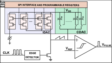
II-A Edge detector
To decouple the pulse-width from that of the pulses, we implemented an Edge Detector block which detects the rising edge of the signal and sends a fixed-width pulse to the transistor , independent of the pulse width [13].
II-B Wide-Range Current Digital to Analog Converter (IDAC)
The wide-range IDAC block of Fig. 2 represents a 7-bit current output binary weighted Digital to Analog Converter (DAC). It consists of identical modular unit cells, combined in a binary weighted fashion to work as p-type current sources. The unit cells are sized appropriately to provide a precise value of current. Both p-type transistors where one being the current source and the other being the gating switch were sized to be of the same width but different lengths. The primary considerations for the sizing were the output resistance, matching, dynamic range and leakage depending on the function of each device. The DAC is biased by an external precise reference current which varies in three steps to cover the large operating range of the circuit as described in table I.
One important consideration for the design of the current DAC is to ensure the current sources are accurate at large output currents, and that the current source transistors are not out of the saturation. The output impedance of the should be high to produce reliable output current with good accuracy. We decided to limit the systematic error to help the system deliver a highly accurate output current. This is especially important, because as as shown in Figure 2, the output is injected to the node whose voltage is changing over time, and the current should not be susceptible to this change through the drain-source voltage across the current sources of the . We verified that the systematic error in the current is under 0.3% of the desired value, if the operating headroom is at least 400-450 mV.
| Pulse Range | ||
|---|---|---|
| 7.8 ns–1 s | 160 A | 10 A–1.28 mA |
| 780 ns–100 s | 1.60 A | 100 nA–12.8 A |
| 78 s–10 ms | 16 nA | 1 nA–128 nA |
We simulated the functionality of the circuit with a wide range of currents, and verified with experimental measurements the correct functionality of the circuit down to the lowest current setting of 1 nA (see Section IV). Typically, the circuit’s systematic error is higher at lower currents, when the p-type transistors operate in weak inversion. However, narrow pulses are needed to characterize the memristive devices. Therefore, in this application scenario to generate narrow pulses, the required current is in the order of magnitude where the IDAC operates in strong inversion saturation.
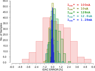
We performed a MonteCarlo simulation to quantify the expected accuracy and quality of this design, as we could not measure through a large set of silicon samples. In this analysis, we quantified the error for five different current settings ranging from the minimum to maximum of the 7-bit IDAC code across different range of operation as described in Table I. The deviation from the target value of the programmed current was calculated as:
| (2) |
where is the actual simulated output current and is the desired output current programmed with the 7-bit code. The results are shown in Fig. 3. For this simulation, we limited the lower current setting of to 100 nA as the MonteCarlo simulation in this technology yields a very large systematic offset (probably arising from inaccurate sub-threshold mismatch models). It can be observed from Fig. 3 that the lower current setting of 100 nA shows the largest error, and the highest current setting of 1.28 mA (required for the narrowest pulse) shows the least error, indicative of its high accuracy. Overall, the combined error of is within 6% for all the current ranges tested, without any calibration process. Extra tuning for higher accuracy is possible by adjusting the capacitance value (trimming).
II-C
The primary capacitor in this system is an 8-bit binary weighted capacitor DAC (). The is constructed out of identical unit DAC cells, carefully laid out to provide a good level of matching among all the elements in the array. The resolution of the is 62.5 fF and the total capacitance we chose for our application is 10 pF. This enables us to adjust the DAC value and correct/trim out any non-idealities in the design with a precision of . As the desired value of 10 pF (maximum value = 16pF) is not exactly at the centre of the DAC code range, we have non-uniform correction range centered around the desired value. However, one could potentially choose the exact center value of this DAC to be the capacitance required for pulse generation by either adjusting the current or the reference voltage as described in Eq. 1.
II-D Hysteretic Comparator
For this application, the primary considerations for a comparator was to have hysteresis to avoid false triggering due to fluctuations on the node the comparator monitors. In addition to this the other main considerations were to have low-offset and high-speed. For the comparator design, we chose a well-known architecture of a hysteretic comparator [14, 15] as shown in Fig. 4. Positive feedback is introduced in this circuit to have hysteresis.

III Implementation and system level simulation
The pulse generator was designed and fabricated in a standard 180 nm technology node. The final design excluding the probe pads occupy an area of 369 m139 m as shown in Fig. 5. The chip microphotograph is shown in Fig. 6.
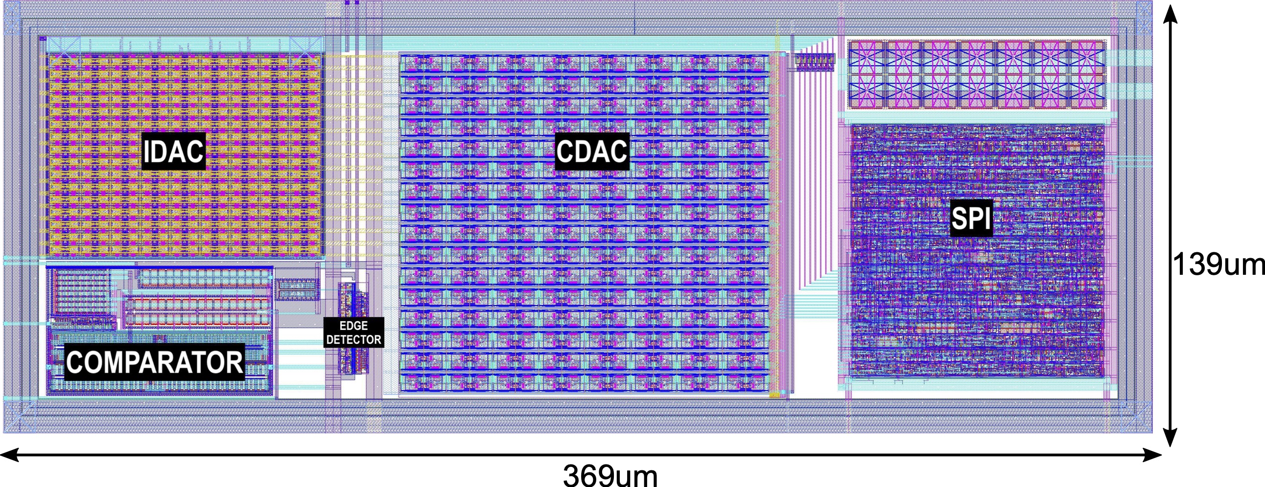
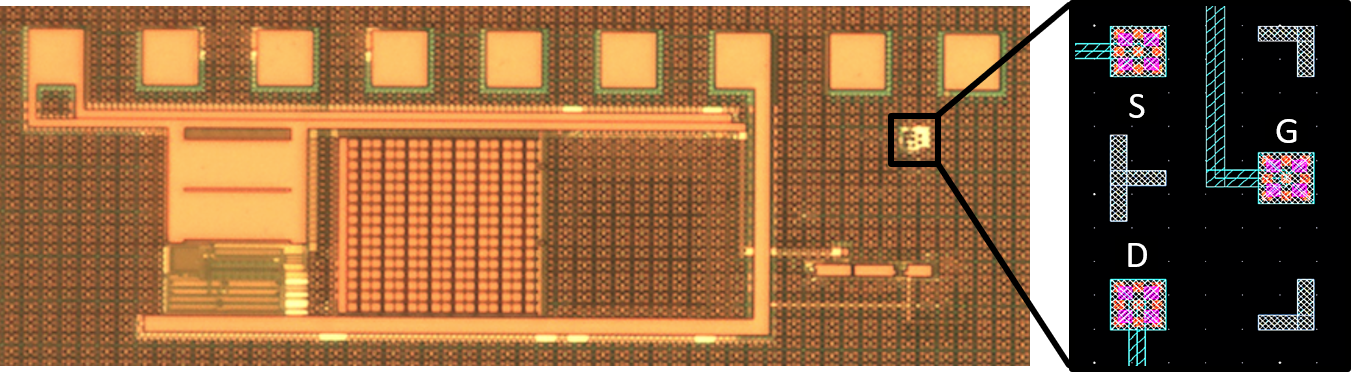
The pulse generator can be programmed using internal Serial Peripheral Interface (SPI) registers. Both and are internally wired to their respective registers which are tightly integrated with rest of the analog circuitry as shown in Fig. 5. The I/Os are wired up to metal probe pads. They are powered and clocked externally through the wafer probing equipment. The FTJs will be fabricated on the same die with Back End Of Line (BEOL) post-processing integration steps. Therefore, the output of the pulse generator is directly connected to the FTJs with on chip low parasitic interconnects and switches.
Table II compares the performance of this work against the implementations designed for similar application. This design can reliably cover a programmable range at least 4 orders of magnitude more than [16], the digital implementation on the same technology node. Although compared to [17], the area benefit of our work is explainable by the smaller technology node and the programming range is 1 order of magnitude less, the accuracy of the pulses in our design across the full programmable range is 2.5% which is not reported in [16] and [17].
IV Hardware setup and electrical characterization
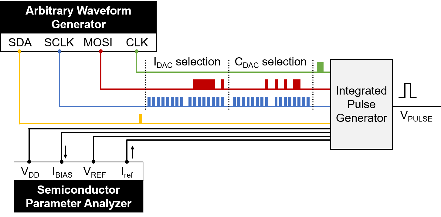
To measure data from the fabricated pulse generator circuit we used a probe-station and applied constant voltages and currents using a Semiconductor Parameter Analyzer (see Fig. 7). The SPI and CLK signals of Fig. 7 were generated using an Arbitrary Waveform Generator.
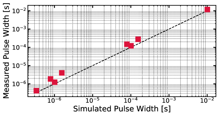
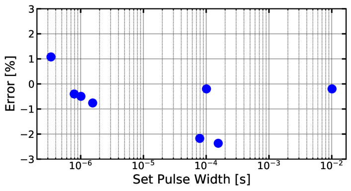
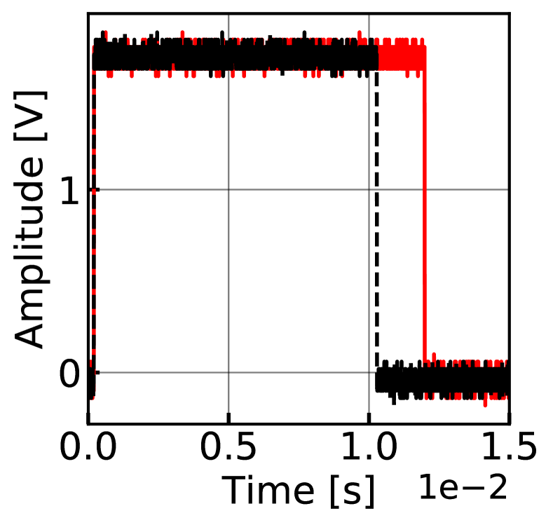
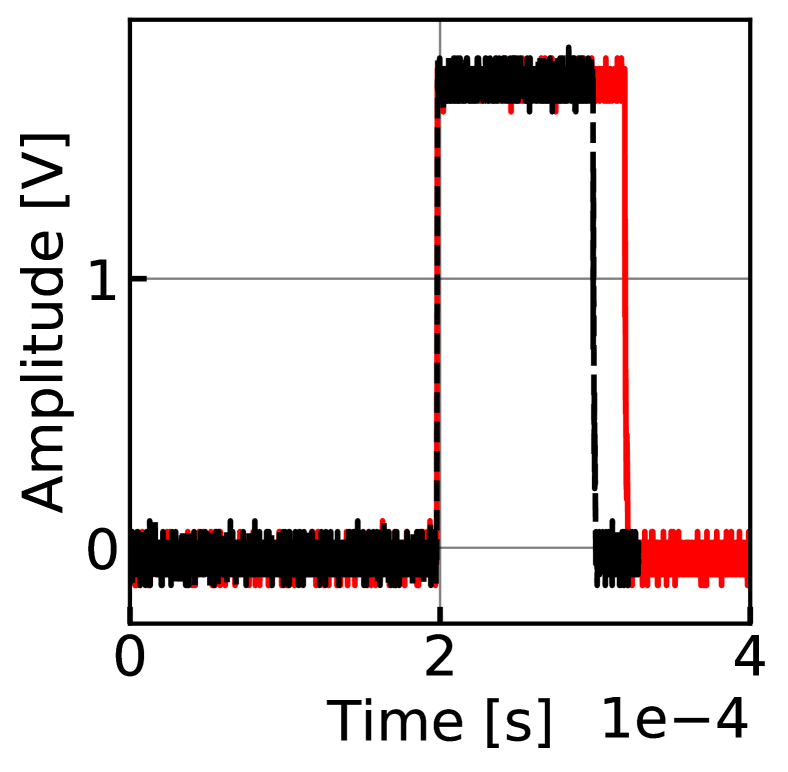
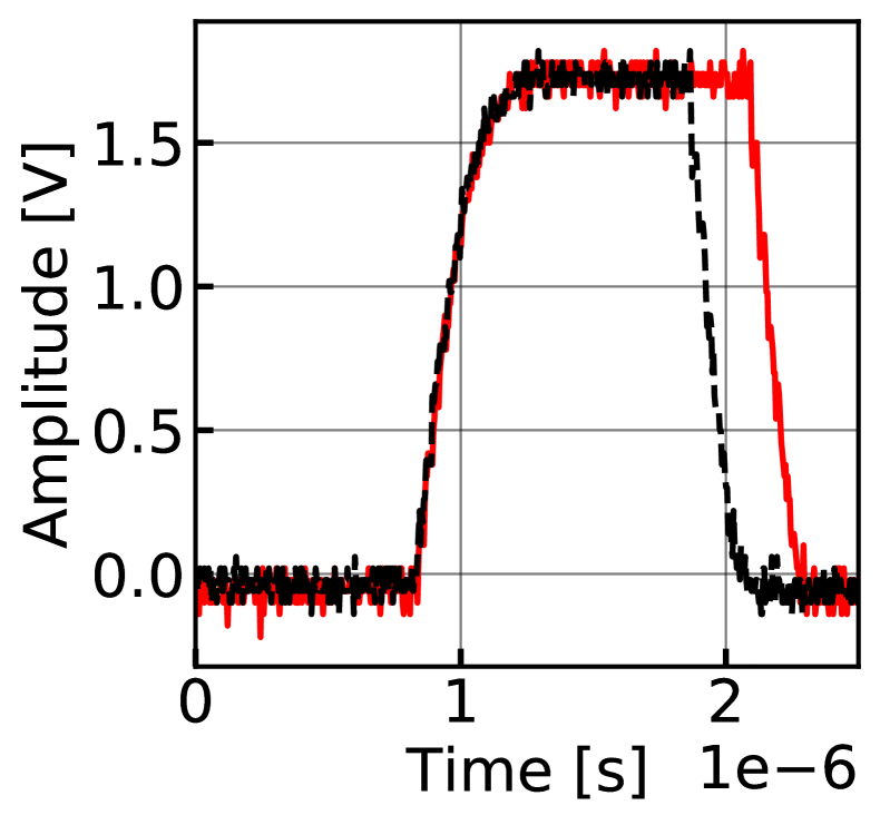
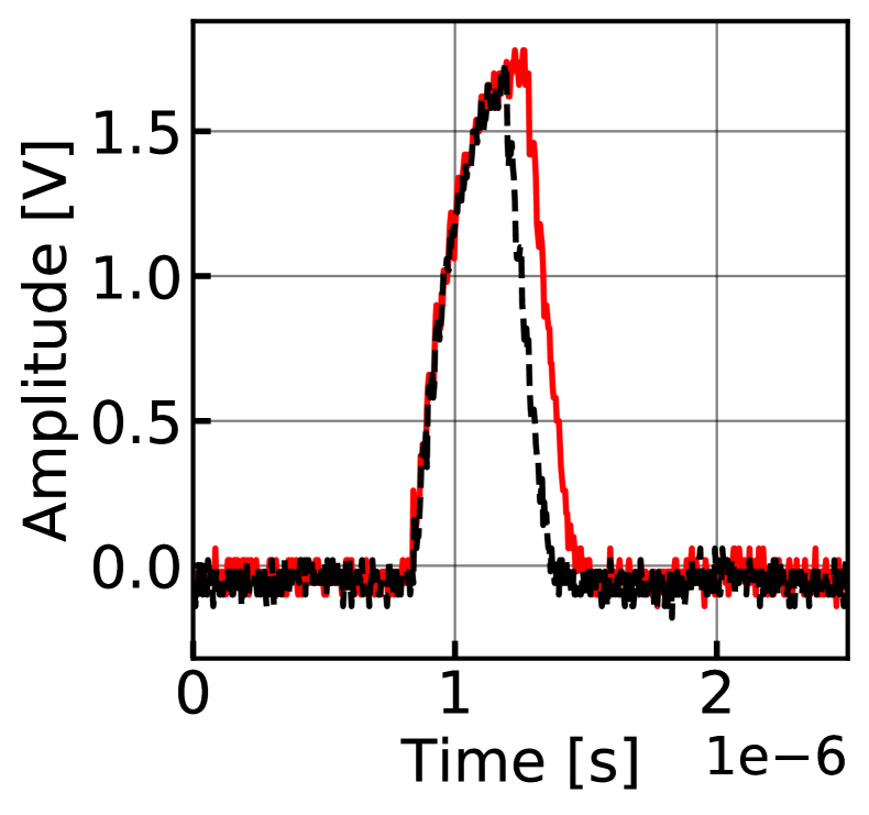
Initially, we biased the circuit using the same parameters used in the circuit simulations to produce pulses of desired widths. However, the fabricated circuits produced outputs that differ significantly from the circuit simulations (Fig. 8(a)). The option of precisely calibrating the capacitance value using the allows accurate pulse widths, with errors below (Fig. 8(b)). Here, only pulses down to 350 ns width could be measured, due to the RC parasitic load induced by the setup. This is confirmed in Fig. 9, showing a selection of waveforms generated by the pulse generator under different conditions. The trend shown in Fig. 8(a) proves that the pulse generator can work at shorter pulse widths. In normal operating conditions, the device to be tested is placed right next to the Pulse Generator, whose photograph, as well as a detail of the contacts for the BEOL-integration of ferroelectric devices, are shown in Fig. 6. In this configuration, the integrated Pulse Generator is no longer limited by the parasitic load, and the generated waveform are expected to be adequate to precisely investigate the switching kinetics of ferroelectric devices.
V Conclusion
We presented an on-chip pulse-generator designed and fabricated in 180 nm technology. We demonstrated pulse generation across 6 orders of magnitude with an error of , while capable of driving relatively high parasitic capacitive loads present in the measurement setup. A low-parasitic on-chip interconnect between the the pulse-generator and the FeFET/FTJ devices placed on the same silicon ensures a reliable delivery of programming pulses with high accuracy. Future work includes exploring performance of the two DACs and their effect on the output pulses. This work is a key enabler for thorough characterization of the FeFETs/FTJs, otherwise limited to the parasitics of the measurement set up.
References
- [1] J. Okuno, T. Kunihiro, K. Konishi, H. Maemura, Y. Shuto, F. Sugaya, M. Materano, T. Ali, M. Lederer, K. Kuehnel, K. Seidel, U. Schroeder, T. Mikolajick, M. Tsukamoto, and T. Umebayashi, “High-endurance and low-voltage operation of 1t1c feram arrays for nonvolatile memory application,” in 2021 IEEE International Memory Workshop (IMW), 2021, pp. 1–3.
- [2] S. Beyer, S. Dünkel, M. Trentzsch, J. Müller, A. Hellmich, D. Utess, J. Paul, D. Kleimaier, J. Pellerin, S. Müller, J. Ocker, A. Benoist, H. Zhou, M. Mennenga, M. Schuster, F. Tassan, M. Noack, A. Pourkeramati, F. Müller, M. Lederer, T. Ali, R. Hoffmann, T. Kämpfe, K. Seidel, H. Mulaosmanovic, E. T. Breyer, T. Mikolajick, and S. Slesazeck, “Fefet: A versatile cmos compatible device with game-changing potential,” in 2020 IEEE International Memory Workshop (IMW), 2020, pp. 1–4.
- [3] B. Max, M. Hoffmann, S. Slesazeck, and T. Mikolajick, “Direct correlation of ferroelectric properties and memory characteristics in ferroelectric tunnel junctions,” IEEE Journal of the Electron Devices Society, vol. 7, pp. 1175–1181, 2019.
- [4] E. Covi, Q. T. Duong, S. Lancaster, V. Havel, J. Coignus, J. Barbot, O. Richter, P. Klein, E. Chicca, L. Grenouillet, A. Dimoulas, T. Mikolajick, and S. Slesazeck, “Ferroelectric tunneling junctions for edge computing,” in 2021 IEEE International Symposium on Circuits and Systems (ISCAS), 2021, pp. 1–5.
- [5] H. Mulaosmanovic, J. Ocker, S. Müller, M. Noack, J. Müller, P. Polakowski, T. Mikolajick, and S. Slesazeck, “Novel ferroelectric fet based synapse for neuromorphic systems,” in 2017 Symposium on VLSI Technology, 2017, pp. T176–T177.
- [6] M. Halter, L. Bégon-Lours, V. Bragaglia, M. Sousa, B. J. Offrein, S. Abel, M. Luisier, and J. Fompeyrine, “Back-end, cmos-compatible ferroelectric field-effect transistor for synaptic weights,” ACS Applied Materials & Interfaces, vol. 12, no. 15, pp. 17 725–17 732, 2020, pMID: 32192333. [Online]. Available: https://doi.org/10.1021/acsami.0c00877
- [7] B. Suresh, M. Bertele, E. T. Breyer, P. Klein, H. Mulaosmanovic, T. Mikolajick, S. Slesazeck, and E. Chicca, “Simulation of integrate-and-fire neuron circuits using hfo¡inf¿2¡/inf¿-based ferroelectric field effect transistors,” in 2019 26th IEEE International Conference on Electronics, Circuits and Systems (ICECS), 2019, pp. 229–232.
- [8] G. Indiveri and S.-C. Liu, “Memory and information processing in neuromorphic systems,” Proceedings of the IEEE, vol. 103, no. 8, pp. 1379–1397, 2015.
- [9] H. Mulaosmanovic, J. Ocker, S. Müller, U. Schroeder, J. Müller, P. Polakowski, S. Flachowsky, R. van Bentum, T. Mikolajick, and S. Slesazeck, “Switching kinetics in nanoscale hafnium oxide based ferroelectric field-effect transistors,” ACS Applied Materials & Interfaces, vol. 9, no. 4, pp. 3792–3798, 2017, pMID: 28071052. [Online]. Available: https://doi.org/10.1021/acsami.6b13866
- [10] M. Materano, P. D. Lomenzo, H. Mulaosmanovic, M. Hoffmann, A. Toriumi, T. Mikolajick, and U. Schroeder, “Polarization switching in thin doped hfo2 ferroelectric layers,” Applied Physics Letters, vol. 117, no. 26, p. 262904, 2020.
- [11] H. Mulaosmanovic, F. Müller, M. Lederer, T. Ali, R. Hoffmann, K. Seidel, H. Zhou, J. Ocker, S. Mueller, S. Dünkel, D. Kleimaier, J. Müller, M. Trentzsch, S. Beyer, E. T. Breyer, T. Mikolajick, and S. Slesazeck, “Interplay between switching and retention in hfo¡sub¿2¡/sub¿-based ferroelectric fets,” IEEE Transactions on Electron Devices, vol. 67, no. 8, pp. 3466–3471, 2020.
- [12] E. Covi, A. Cabrini, L. Vendrame, L. Bortesi, R. Gastaldi, and G. Torelli, “On-wafer analog pulse generator for fast characterization and parametric test of resistive switching memories,” IEEE Transactions on Semiconductor Manufacturing, vol. 27, no. 2, pp. 134–150, 2014.
- [13] N. Weste, CMOS VLSI Design: A Circuits and Systems Perspective. Addison Wesley, 2011.
- [14] D. Allstot, “A precision variable-supply cmos comparator,” IEEE Journal of Solid-State Circuits, vol. 17, no. 6, pp. 1080–1087, 1982.
- [15] P. Allen and D. Holberg, CMOS Analog Circuit Design, ser. The Oxford Series in Electrical and Computer Engineering. OUP USA, 2011.
- [16] S. Lee and H. Yoo, “Configurable digital pulse generator for neuromorphic devices,” in 2021 International Conference on Electronics, Information, and Communication (ICEIC), 2021, pp. 1–3.
- [17] H. Erfanijazi, T. Serrano-Gotarredona, and B. Linares-Barranco, “Novel programmable single pulse generator for producing pulse widths in different time scales,” in 2021 International Conference on Content-Based Multimedia Indexing (CBMI), 2021, pp. 1–6.