Full-zone Persistent Spin Textures with Giant Spin Splitting in Two-dimensional Group IV-V Compounds
Abstract
Persistent spin texture (PST), a property of solid-state materials maintaining unidirectional spin polarization in the momentum -space, offers a route to deliver the necessary long carrier spin lifetimes through the persistent spin helix (PSH) mechanism. However, most of the discovered PST locally occurred in the small part around certain high symmetry -points or lines in the first Brillouin zone (FBZ), thus limiting the stability of the PSH state. Herein, by symmetry analysis and first-principles calculations, we report the emergence of full-zone PST (FZPST), a phenomenon displaying the PST in the whole FBZ, in the two-dimensional group IV-V ( = Si, Sn, Ge; = Bi, Sb) compounds. Due to the existence of the in-plane mirror symmetry operation in the wave vector point group symmetry for the arbitrary in the whole FBZ, fully out-of-plane spin polarization is observed in the -space, thus maintaining the FZPST. Importantly, we observed giant spin splitting in which the PST sustains, supporting large SOC parameters and small wavelengths of the PSH states. Our analysis demonstrated that the FZPST is robust for the non-degenerate bands, which can be effectively controlled by the application of an external electric field, thus offering a promising platform for future spintronic applications.
-
February 2021
1 Introduction
The study of relativistic effects in solids, i.e., the spin-orbit coupling (SOC), has attracted increasing interest in the field of spintronics since it allows for manipulation of an electron’s spin degree of freedom without additional external magnetic field [1]. Many intriguing SOC-related phenomena were observed, including spin relaxation [2, 3], spin Hall effect [4], spin galvanic effect [5], and spin ballistic transport [6]. In a system lacking inversion symmetry, the SOC induces momentum ()-dependent spin-orbit field (SOF), , where is the electric field originated from the crystal inversion asymmetry and is the momentum, that lifts Kramer’s spin degeneracy and leads to the nontrivial -dependent spin textures of the spin-split bands through the so-called Rashba [7] and Dresselhaus [8] effects. In particular, the Rashba effect attracted much attention since it can be manipulated electrically to produce non-equilibrium spin polarization [9, 10], which plays an important role in the spin-field effect transistors (SFET) [11].
Practically, materials with a strong Rashba effect are desirable in spintronic applications since a large Rashba SOC parameter is in favor of room temperature device operations [12]. However, the strong Rashba SOC is also known to induce the undesired effect of causing spin decoherence, which plays a detrimental role in the spin lifetime [13]. Due to the -dependent SOF, electron scatterings by defect and impurity randomize the spin in a diffusive transport regime, which induces the fast spin decoherence through the Dyakonov-Perel spin relaxation mechanism [13], and hence limits the performance of the spintronics functionality. This problem can further be resolved by designing the materials supporting unidirectional SOF. Under the unidirectional SOF, the spin polarization is unidirectionally oriented in the -space, resulting in the so-called persistent spin texture (PST) [14, 15], thus enabling long-range spin transport without dissipation through persistent spin helix (PSH) mechanism [16, 15, 17]. Previously, GaAs/AlGaAs [18, 19] and InGaAs/InAlAs [20, 21, 22] quantum well (QW) heterostructures have been reported to demonstrate the emergence of the PSH state arising from a balance between the strength of the Rashba and Dresselhaus SOCs; however, these artificial structures require atomic precision by tuning the QW width and carefully controlled carrier densities through doping level and applied external electric field.
Recently, a different approach for achieving the PST has been proposed, imposing the specific symmetry of the crystal for the systems having a crystallographic polar axis to preserve the unidirectional SOF [23]. While it remains to be confirmed experimentally, this approach allows us to design the PST without requiring the fine-tuning between the Rashba and Dresselhaus SOCs. This is particularly achieved on the class of materials exhibiting intrinsic spontaneous electric polarization as previously reported on bulk ferroelectric BiInO3 [23], CsBiNb2O7 [24], layered ferroelectric oxide Bi2WO6 [25], and several two-dimensional (2D) ferroelectric systems including WO2Cl2 [26], Ga(=Se, Te; =Cl, Br, I) [27, 28], hybrid perovskite benzyl ammonium lead-halide [29], and group-IV monochalcogenide [30, 31, 32, 33, 34]. More recently, the symmetry-protected PST with purely cubic spin splitting has also been reported in bulk materials crystallizing in the and point groups [35]. In addition, the PST driven by the lower symmetry of the crystal has also been reported on wurtzite ZnO [100] surface [36] and several 2D transition metal dichalcogenides (TMDCs) with the line defect [37, 38]. Although the symmetry-enforced PSTs have been extensively studied, most of them locally occurred in the small part around the high symmetry points or lines in the first Brillouin zone (FBZ) [23, 24, 26, 27, 28, 30, 31, 32, 33, 34, 35]. This implies that the spin deviation away from the uniaxial SOF appears for the larger region in the FBZ, which has a considerable effect to induce the significant spin scattering and hence limits the stability of the PSH states [23, 39]. Therefore, finding novel structures supporting the PST covering a substantially large region in the FBZ is highly desirable, which is important to produce a stable PSH state without controlling the Fermi level in the specific FBZ region.
In this paper, through symmetry analysis and first-principles density-functional theory (DFT) calculations, we show that the PST could exist in the whole FBZ of the 2D group IV-V ( = Si, Sn, Ge; = Bi, Sb) compounds. We dub this phenomenon the full-zone PST (FZPST). We found that the FZPST observed in the present systems is characterized by fully out-of-plane spin polarization in the -space, which is enforced by the in-plane mirror symmetry operation in the wave vector point group symmetry for the arbitrary in the whole FBZ. More importantly, the observed FZPST exhibits giant spin splitting, which is particularly visible around the points in the conduction band minimum, thus resulting in large SOC parameters and small wavelengths of the PSH states. Our analysis derived from the invariant method [40, 41] confirmed that this FZPST is robust for the non-degenerate bands, which can be sensitively tuned by an external electric field. Finally, a possible application of the FZPST in the present system for spintronic devices will be highlighted.
2 Computational Details
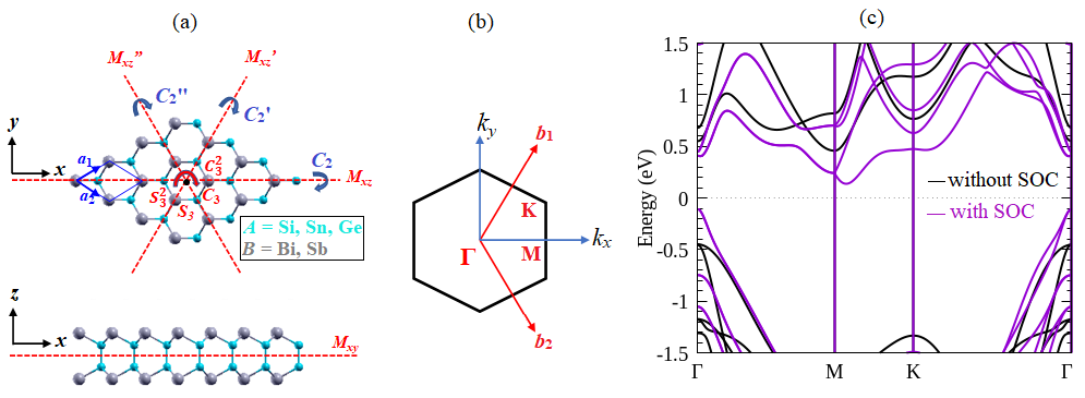
Our DFT calculations were carried out based on norm-conserving pseudo-potentials and optimized pseudo-atomic localized basis functions [42] implemented in the OPENMX code [43, 44, 45, 45]. The exchange-correlation functional was treated within generalized gradient approximation by Perdew, Burke, and Ernzerhof (GGA-PBE) [46, 47]. The basis functions were expanded by the linear combination of multiple pseudo atomic orbitals generated using a confinement scheme [44, 48, 45], where two -, two -, two -character numerical pseudo atomic orbitals were used. We applied a periodic slab to model the monolayers (MLs), where a sufficiently large vacuum layer (35 Å) was used to avoid the spurious interaction between the slabs [Fig. 1(a)]. The -point mesh was used to discretize the FBZ [Fig. 1(b)]. The energy convergence criterion was set to eV during the structural relaxation. The lattice and positions of the atoms were optimized until the Hellmann-Feynman force components acting on each atom were less than 1 meV/Å. The vibrational properties and the phonon dispersion relations were acquired via the small-displacement method using the PHONOPY code [49]. Ab-initio molecular dynamics (AIMD) simulations were also carried out to examine the thermal stability of the MLs by using a 4×4×1 supercell consisting of 64 atoms at room temperature (300 K) with a total simulation time of 6 ps.
The spin textures in the -space were evaluated by using the spin density matrix of the spinor wave functions obtained from the DFT calculations [50]. As we applied previously on various 2D materials [27, 28, 30, 38, 31, 33, 51, 52], we deduced the spin vector component (, , ) of the spin polarization in the reciprocal lattice vector from the spin density matrix, , calculated using the following relation,
| (1) |
where () is the spin index ( or ) and is the band index. Here, is the spinor Bloch wave function, which is obtained from the OpenMX calculations after self-consistent is achieved.
3 Results and Discussion
3.1 Symmetry-enforced FZPST in the 2D non-magnetic systems
First, we start our discussion by analyzing the FZPST from the symmetry perspective. It has been generally understood that the classification of the materials having spin-orbit-induced spin splitting and spin polarization is usually determined by the crystallography point group symmetry (CPGS) such as polar and non-polar crystal classes. However, for a fixed CPGS, a journey through the FBZ from one point to another leads to a change in the wave vector point group symmetry (WPGS). Consequently, a significant change of the spin textures, defined as the expectation value of the spin polarization vector in the -space, may occur [53]. Since the is bound to be parallel to the rotational axis and perpendicular to the mirror plane, the symmetry operation types in the WPGS impose symmetry restriction on . Therefore, the FZPST is achieved as long as the WPGS keeps the unidirectional spin polarization invariant in the whole FBZ. To realize the symmetry-protected FZPST, there must exist a symmetry operator of the WPGS protecting the wave vector invariant in the whole FBZ. By defining as the symmetry operator of the WPGS, the representation of , , can be determined through the following relation, . Therefore, the allowed spin polarization direction, , at given can be obtained by the invariant condition of the under the symmetry opertor as follows, .
Now, let us consider the 2D crystalline systems where the out-of-plane direction is chosen to be oriented along the -axis. In this case, the FBZ is a 2D plane with . For this 2D system, we find that only the identity and in-plane mirror symmetry operations maintain the point being invariant in the whole FBZ. Accordingly, the allowed under the restriction of these symmetry operations enforced to unidirectionally oriented along the out-of-plane () direction in the whole FBZ through the following transformation, , leading to the FZPST. We emphasized here that for non-magnetic 2D crystalline systems, all the points are invariant under time-reversal symmetry operation . For a given inversion symmetry operation , we can construct an anti-unitary operator, , which flips the spin polarizatrion vector , so that for any in the FBZ. Therefore, we conclude that the FZPST could exist in the 2D non-magnetic systems if and only if the wave vector in the whole FBZ has the in-plane mirror symmetry but without inversion symmetry .
| N | N | N | Y | Y | Y | N | N | Y | N | N | Y | N | N | |
| N | Y | N | N | Y | N | N | N | N | N | N | Y | N | N | |
| FZPST | N | N | N | Y | N | Y | N | N | Y | N | N | N | N | N |
| Y | N | N | Y | N | N | Y | N | N | Y | N | Y | N | ||
| Y | N | N | Y | N | N | N | Y | N | Y | N | Y | N | ||
| FZPST | N | N | N | N | N | N | Y | N | N | N | N | N | N |
Finally, we search the possible FZPST in the 2D crystalline system identified using the criteria whether the CPGS containing (Y) or not containing (N) both the in-plane mirror symmetry and inversion symmetry () operations under the guidance of Table 1. When the CPGS contains the in-plane mirror symmetry operation, the WPGS for the point in the whole FBZ should be invariant under this symmetry operation. Therefore, we find that the following CPGS of the 2D crystalline systems is possible to maintain the FZPST including , , , and .
In the next section, we discuss our results from the first-principles DFT calculations on the group IV-V ML compounds to confirm the above-predicted FZPST.
3.2 FZPST in 2D group IV-V compounds
3.2.1 Structural symmetry, stability, and electronic properties.
It has been previously reported that a combination between group IV elements, ( = Si, Sn, Ge), and group V elements, ( = Bi, Sb), forms a stable 2D layered compounds [54, 55, 56]. These compounds consists of covalently bonded quadruple atomic layers in a sequence, forming a trigonal prismatic structure because atoms are coordinated in the form of a triangular prism with respect to the dimer, similar to the 2H-phase of the TMDCs MLs [57, 58, 52, 59]. The atomic structure and corresponding to the FBZ are schematically shown in Figs. 1(a) and (b), respectively. From symmetry point of view, the crystal symmetry of the ML compounds has space group. There are six classes of the symmetry operation making the structure of the MLs invariant including identity (), in-plane mirror reflection (), out-of-plane mirror reflection (, , ), two-fold rotation around the axis parallel to the plane (, , ), three-fold rotation around the -axis (, ), and three-fold improper rotation around the -axis (, ) [see Fig. 1(a)]. Therefore, the CPGS of the MLs belongs to point group. The optimized structural-related parameters including lattice constant , bond distances, and bond angles in the MLs are presented in Table SI in the the Supporting Information [60], and overall are in a good agreement with previous results [55, 56, 54].
To confirm the stability of the MLs, several assessments are carried out including cohesive energy (), phonon dispersion bands, and the AIMD simulation. All the calculated results confirmed that the optimized ML compounds are energetically, dynamically, and thermally stable; see the Supporting Information [60]. It has been reported previously that several layered compounds ( = Si, Ge; = As, P) have been experimentally synthesized in the bulk form [61], which opens an opportunity for the realization of these compounds in the 2D form. Considering the similar structural symmetry and stability, the experimental realization of the MLs (= Si, Ge, Sn; = Sb, Bi) is highly plausible.
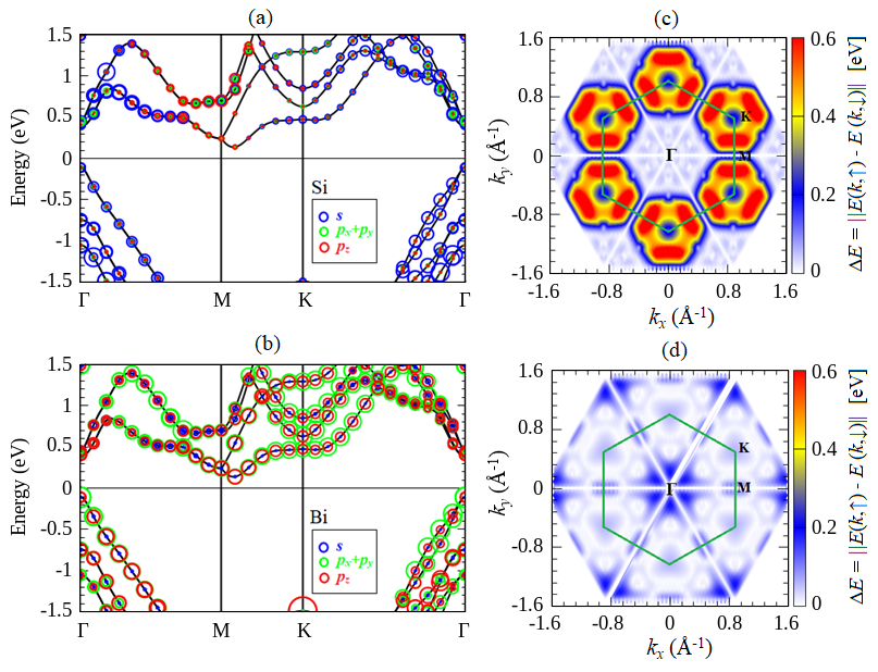
To characterize the electronic properties of the MLs, we show in Fig. 1(c) the calculated band structure of the Si2Bi2 ML as a representative example, while the band structure for other members of the MLs are presented in Figure S3 in the Supporting Information [60]. Consistent with previous reports [54, 55, 56], the Si2Bi2 ML is an indirect semiconductor where the valence band maximum (VBM) is located on the point, while the conduction band minimum (CBM) lies on the point. When the SOC is taken into account, the CBM resides between and points, thus maintaining the indirect bandgap. Our calculated orbital-resolved the band projected to the atoms confirmed that the CBM is mainly originated from the contribution of Bi- and Bi- orbitals, while the strong admixture of Bi-, Bi-, and Si- orbitals contributes significantly to the VBM [Figs. 2(a)-(b)].
Introducing the SOC induces a sizable band splitting due to the inversion symmetry breaking of the crystal [Fig. 1(c)]. This splitting is particularly visible for points and lines located in the proximity of the band edges near the Fermi level, except for time-reversal-invariant points at and points, and high symmetry line at the line. To quantify the spin-split bands, we show in Figs. 2(c)-(d) the spin-splitting energy of the CBM and VBM mapped along the entire region of the FBZ. Consistent with the band degeneracy along the line, zero spin splitting is clearly visible for , where and is measured from . Interestingly, we identify a strongly anisotropic spin-splitting around the point in the CBM where the maximum spin-splitting energy up to 0.72 eV is observed along the line [Fig. 2(c)]. This giant spin splitting is indeed larger than that observed on several TMDCs MLs [0.15 eV–0.55 eV] [57, 58, 52, 62, 63], which is mainly originated from the strong admixture of the in-plane (Bi-, Si-) and out-of-plane (Bi-, Si-) orbitals [Figs. 2(a)-(b)]. Remarkably, The giant spin splitting observed in the present system is certainly sufficient to ensure the proper function of spintronic devices operating at room temperature [12].
3.2.2 DFT analysis of the FZPST.
Now, we discuss the emergence of the FZPST in the Si2Bi2 ML obtained from the DFT calculation. The FZPST can be observed from the spin polarization of the spin-split bands in the whole FBZ. However, before we show our DFT results, we first clarify the existence of the FZPST by identifying the WPGS of the in the whole FBZ. As previously mentioned that the CPGS of the MLs belongs to the point group, thus the WPGS of the in the FBZ should contain some of the symmetry operations in the point group. In Table 2, we list the possible WPGS of the corresponding to the symmetry operations at the high symmetry points and lines in the FBZ. We find that the WPGS of the in the whole FBZ belongs to point group containing and symmetries, thus the FZPST should exist in the MLs having fully out-of-plane spin polarization.
| point | WPGS | symmetry operations | ||||
|---|---|---|---|---|---|---|
| , , (, , ), (, , ), (, ), (, ) | ||||||
| , , , | ||||||
| , , (, ), (, ) | ||||||
| , , , | ||||||
| , | ||||||
| , | ||||||
| Whole FBZ | , |

Figs. 3(a)-(c) shows spin-resolved projected to bands along the line in the FBZ calculated for the Si2Bi2 ML. We find that all the spin-split bands in the whole FBZ are fully characterized by the out-of-plane spin component () [Fig. 3(c)], while the contribution of the in-plane spin components (, ) is almost zero [Figs. 3(a)-(b)]. This indicates that the spin polarization direction is locked being oriented in the fully out-of-plane direction, leading to the FZPST; consistent with symmetry analysis. We noted here that we have identified the significant spin polarization at the degenerated bands along the line [Figs. 3(a)-(c)]. However, due to the equal population of the spin polarization between the and spin-polarized states in the degenerated bands along the the line, the net spin polarization becomes zero; see Fig. S4 in the Supporting Information [60]. Thus, the FZPST is robust for the non-degenerate bands.
The emergence of the FZPST in the present system shows that the unidirectional out-of-plane SOF is preserved covering the whole FBZ. In such a situation, electron motion accompanied by the spin precession around the uniaxial SOF lead to a spatially periodic mode of the spin polarization forming a highly stable persistent spin helix (PSH) state [16, 14, 15, 17] as schematically shown in Fig. 3(b). Due to spin rotational symmetry in the PSH state [16], the corresponding spin-wave mode protects the spins of the electrons from dephasing, which is robust against spin-independent scattering, and renders an extremely long spin lifetime by suppressing the DP spin relaxation [13]. Therefore, the present systems enable long-range spin transport without dissipation [17], and hence promising for efficient spintronics devices.
Next, we briefly comment on the main difference between the PST found in the present system compared with that reported in the previous studies. There are two main scenarios to achieve the PST: (i) by fine-tuning the strength of the linear Rashba and Dresselhaus SOCs [16, 14, 15, 17], or (ii) by imposing the specific CPGS for the systems exhibiting crystallographic polar axis [23]. Although the former approach was demonstrated on various semiconductor heterostructures [18, 19, 20, 22], several problems impede the practical application due to the stringent condition for achieving an equal strength of the Rashba and Dresselhaus SOCs. On the other hand, the latter approach may provide an advantage for realizing the PST since the condition of the equal strength of the Rashba and Dresselhaus SOC can be eliminated. However, in addition to producing the local PST in a small part of the FBZ, this approach is limited only for the systems having polar crystallographic axis as previously reported on several bulk ferroelectric materials including BiInO3 [23], CsBiNb2O7 [24], layered ferroelectric oxide Bi2WO6 [25], and 2D ferroelectric systems such as WO2Cl2 [26], Ga(=Se, Te; =Cl, Br, I) [27, 28], hybrid perovskite benzyl ammonium lead-halide [29], and group-IV monochalcogenide [30, 31, 32, 33, 34]. In contrast, for our system, there is no crystallographic polar axis observed in the crystal structure, thus the PST is mainly determined by the WPGS rather than by the CPGS [53]. In addition, the PST observed in the present system covers the whole of the FBZ, which is expected to be more beneficial to producing a highly stable PSH state.
3.2.3 Effective Hamiltonian.
To further clarify the emergence of the FZPST, we then focus our attention on the bands around the point in the CBM due to the large spin splitting as highlighted in Fig. 3(e). Since we have identified the anisotropic nature of the spin splitting around the point [see Fig. 2(c)], it is expected that the spin-split Fermi line at a constant-energy cut should be highly anisotropic. Our calculated Fermi line measured at a constant-energy cut of 0.1 eV above degenerated states at the point in the CBM confirmed the anisotropic spin-split Fermi line, where the center of two spin-split Fermi loops are displaced along the () direction from their original point [Fig. 3(f)]. It is also found that these Fermi loops exhibit perfect PST where opposite spin components between the inner and outer loops are observed [Fig. 3(f)], which is also consistent with spin-resolved projected to the band along the line shown in Fig. 3(e). These typical Fermi lines as well as the PST observed around the points are similar to the [110]-Dresselhaus model supporting the PSH state demonstrated previously on the [110]-oriented semiconductor QW [16] and several 2D systems such as WO2Cl2 [26], Ga(=Se, Te; =Cl, Br, I) [27], and group IV monochalcogenides [33, 34].
To analyze the anisotropic spin splitting and PST around the point, we derive an effective Hamiltonian model using the invariant method obtained from the symmetry analysis [40, 41]. For the particular high symmetry point in the FBZ, the WPGS of the is characterized by a point group , where the matrix representation for the chosen basis functions is given by , where is the symmetry operations in the WPGS. The derived Hamiltonian should satisfy the following invariant condition:
| (2) |
| Symmetry | Invariants | ||
|---|---|---|---|
| Operations | |||
| () | |||
| , , , , | |||
| , , , | |||
| , , , |
Given that the band dispersion around the point in the CBM is mainly composed of Bi- orbitals [Fig. 2(b)], we can ignore other orbitals when constructing the model. Based on these orbitals, we construct the spinor wave functions to obtain the matrix forms of the symmetry operations in the momentum and spin spaces. Since the WPGS at the point belongs to point group [see Table 2], both the and can be transformed according to the symmetry operations of this point group. The transformation rules for the and are presented in Table 3. Here, all the invariant terms of the Hamiltonian have listed in the form of product between the and components and then select those specific terms which are invariant under all symmetry operations as indicated by the underlined terms in the right column in Table 3. Finally, we can write the possible term of the Hamiltonian including the Rashba and Dresselhaus terms as
| (3) |
Here, is the Hamiltonian of the free electrons with eigenvalues , where and are effective mass of electron evaluated from the band dispersion along the and directions, respectively. Since our 2D system is lied on the plane, the term in Eq. (3) is naturally disappeared, thus the effective Hamiltonian can further be expressed as
| (4) |
On diagonalizing Eq. (4), we obtain the eigenstates
| (5) |
and
| (6) |
and corresponding to the eigenenergies
| (7) |
The spin polarization in the -space can be evaluated from the expectation values of the spin operators, i.e., , where is the electron’s eigenstates. By using given in Eqs. (5) and (6), we obtain that
| (8) |
This shows that the spin polarization is locked being oriented in the out-of-plane directions, consistent with the spin-resolved projected bands shown in Figs. 3(e).
In addition, we noted here that Eq. (7) represents the dispersion of the spin split bands around the original point ( point) exhibiting strongly anisotropic splitting, i.e., the energy bands are lifted along the direction ( line) but are degenerated along the direction ( line), which is consistent with the spin splitting map presented in Fig. 2(c). Interestingly, Eq. (7) leads to the following shifting property, , where is the shifting wave vector expressed by
| (9) |
This implies that the band dispersion at a constant-energy cut shows two Fermi loops whose centers are displaced along the (M-K line) direction from their original point ( point) by , which is in a good agreement with the Fermi lines shown in Fig. 3(f). Overall, the consistency of the band splitting, Fermi lines, and spin polarization around the point obtained from the DFT and effective Hamiltonian model justifies the reliability of our method.
To further quantify the PST around the point in the CBM, we here calculate the spin-orbit strength parameter, , by numerically fitting of Eq. (7) to the band dispersion along the line obtained from our DFT results. In Table 4, we summarize the calculated values of for all compounds of the MLs and compare these results with a few selected PST systems previously reported on several 2D materials. Taking Si2Bi2 ML as an example, we find that that the calculated is 2.39 eVÅ, which is comparable with that reported on 2D PST materials including Ga (=Se, Te; =Cl, Br, I) MLs (0.53 - 2.65 eVÅ) [27] and various 2D group IV monochalcogenide such as Ge ( = S, Se, Te) MLs (3.10 - 3.93 eVÅ) [30], and layered SnTe (1.28 - 2.85 eVÅ) [31, 32, 33, 34]. However, this value is much larger than that predicted on WO2Cl2 ML (0.90 eVÅ) [26] and transition metal dichalcogenide MLs with line defect such as PtSe2 (0.20 - 1.14 eVÅ) [38] and (Mo,W) (=S, Se) (0.14 - 0.26 eVÅ) [37].
| 2D materials | (eVÅ) | (nm) | Reference |
|---|---|---|---|
| ML compounds | |||
| Si2Sb2 | 0.63 | 11.62 | This work |
| Ge2Sb2 | 0.72 | 8.61 | This work |
| Sn2Sb2 | 0.80 | 6.50 | This work |
| Si2Bi2 | 2.39 | 2.15 | This work |
| Ge2Bi2 | 2.41 | 2.13 | This work |
| Sn2Bi2 | 2.55 | 2.02 | This work |
| Group IV Monochalcogenide | |||
| (Sn,Ge) (= S, Se, Te) | 0.07 - 1.67 | - 1.82 | Ref. [33] |
| Ge (= S, Se, Te) | 3.10 - 3.93 | 6.53 - 8.52 | Ref. [30] |
| Layered SnTe | 1.28 - 2.85 | 8.80 - 18.3 | Ref. [34] |
| Strained SnSe | 0.76 - 1.15 | Ref. [32] | |
| SnSe- (= Cl, Br, I) | 1.60 - 1.76 | 1.27 - 1.41 | Ref. [31] |
| Defective 2D TMDCs | |||
| line defect in PtSe2 | 0.20 - 1.14 | 6.33 - 28.19 | Ref. [38] |
| line defect in (Mo,W)(S,Se)2 | 0.14 - 0.26 | 8.56 - 10.18 | Ref. [37] |
| Other 2D ML | |||
| WO2Cl2 | 0.90 | Ref. [26] | |
| Ga (=Se, Te; =Cl, Br, I) | 0.5 - 2.65 | 1.2 - 6.57 | Ref. [27] |
We pointed out here that the observed PST with a large spin-orbit strength parameter, , is expected to induce the highly stable PSH states. Therefore, it is possible to estimate the wavelength of the PSH, , defined as [see Fig. 3(d)], where the shifting wave vector is evaluated from Eq. (9). The resulting wavelength for all members of the ML compounds are listed in Table 4. It is found that the smaller is achieved for the MLs with larger . In particular, we find a small value of for Si2Bi2 ML (2.15 nm), which is smaller than that reported on several 2D group IV monochalcogenide [30, 31, 33, 34] and defective transition metal dichalcogenides [38, 37] [see Table 4]. Typically, the small wavelength of the PSH state observed in the present system is on the scale of the lithographic dimension achieved by the recent semiconductor industry [64], which is promising for miniaturization and highly scalable spintronics devices.
Thus far, we have found that the FZPST is achieved in the MLs of compounds. In particular, the PST with the large spin splitting is observed for the Si2Bi2 ML ( eVÅ) in the CBM around the point, indicating that the PSH state is achieved when the electron carriers are optically injected into the unoccupied state. Moreover, motivated by the observation of the valley Hall effect previously reported on the 2D TMDCs [65], it is possible to observe a spin Hall effect in the ML compounds based on the emergence of the PST. Due to the large spin splitting along the line ( direction) in the CBM [Figs. 1(c) and 3(c)], the spin polarization is expected to occur in the two states located at the and near the CBM; see the spin-resolved projected to the Fermi lines shown in Fig. 3(f). Accordingly, large Berry curvatures with opposite signs are induced. Therefore, it is possible to create an imbalanced population of the spins of electrons in these two states by using polarized optical excitation, and hence a spin Hall current can be detected.
We noted here that to access experimentally the electronic states displaying the PST, the problem of Fermi-level tuning is indispensable due to the semiconductor nature of the electronic state of the MLs. Here, the application of an external electric field could be a promising method for tuning the Fermi level in the previously reported 2D materials [66, 67, 68]. However, introducing the electric field may disturb the stability of the PST due to the breaking of the crystal symmetry [30]. In the next subsection, we will show that how the FZPST observed in the present system can be sensitively affected by the external electric field, thus offering a promising platform for spintronic devices such as the SFET.
3.2.4 The Role of external electric field.

Now, we turn our attention to examining the effect of the external electric field on the FZPST of the MLs. Here, we introduce the external out-of-plane electric fields, , oriented along the directions as schematically shown in Fig. 4(a). When the is applied, both the rotational and in-plane mirror symmetries are broken. The breaking of the particular symmetry operations under the influence of the external electric fields is expected to strongly modify the electronic properties of the MLs. In fact, an electronic transition from indirect semiconductor to metallic states is observed when the external electric fields are introduced; see Fig. S5 in the Supporting Information [60], which is attributed to the modulation of the hybridization states between the Bi-, Si-, and Si- orbitals around the proximity of the band edges (CBM and VBM) near the Fermi level [see Figs. 2(a)-(b)]. The electronic transition states driven by the electric fields observed in the present system are similar to that reported previously on the various 2D materials [66, 67, 68].
We noted here that the application of the external electric fields also induces modification of the spin-splitting properties of the Si2Bi2 ML. Fig. 4(b) shows the spin-resolved projected to the bands of the Si2Bi2 ML under the external electric fields of 0.2 V/Å. Due to the breaking of the rotational symmetry of the crystal by the [Fig. 4(a)], substantially small band splitting is induced in the bands along the line, except for the point at the and points due to time reversibility [Fig. 4(b)]. However, the large spin splitting remains for the bands along the line. Since the in-plane mirror symmetry is already broken by the external out-of-plane electric field , significant in-plane spin components (, ) are induced in the spin-split bands [Fig. 4(b)], thus breaking the FZPST. Because the large band splitting is located close to the Fermi level, the application of the external electric field may be a hint for future spintronics applications.
To further analyze the spin-splitting properties of the Si2Bi2 ML under the out-of-plane external electric fields , we consider the spin-split polarized bands around the point in the CBM as highlighted in Fig. 5(a). By adopting the invariant method [40, 41], the effective Hamiltonian around the point in the CBM including the electric field contribution can written as
| (10) | |||||
| (11) |
Here, is the Hamiltonian without an external electric field, while represents the Hamiltonian induced by an external electric fields, , characterized by the parameter , where is the spinor Bloch wave function of the unoccupied states around the point in the CBM. By setting the and axis along the and lines, respectively, the Hamiltonian of Eq. (11) leads to the eigenenergies:
| (12) |
where , and . We can see that application of splits the band degeneracy along the () due to the non-vanishing -terms in Eq. (12), which is consistent with the band dispersion presented in Figs. 4(b). The explicit expressions of spin expectation values for Hamiltonian of Eq. (11) can be easily derived from the explicit form of the electron eigenstates, reading
| (13) |
where . It is clearly seen that introducing induces the in-plane spin components (, ) terms in Eq. (13), which is also agree-well with the spin-resolved bands obtained from the DFT results shown in Fig. 4(b).
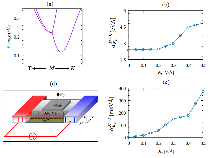
To further characterize the spin-splitting properties of the Si2Bi2 ML under the influence of the external out-of-plane electric fields, we show in Figs. 5(b)-(c) the electric field-dependent of the SOC parameters (, ). Here, the and parameters are obtained by numerically fitting the energy dispersion of the Eq. (12) to the DFT bands along the () and () lines, respectively, in the CBM around the point. Interestingly, we observed a strong enhancement of the particular SOC parameters when the external electric fields are introduced. in deed, a sharp increase of more than 100% occurs for the parameters when the are larger than 0.35 V/Å [Fig. 5(b)]. The same trend also holds for the parameters, see Fig. 5(c). Such a strong enhancement of the SOC parameters by the electric fields helps precisely control the spin precession [69], which is important for the operation in the SFET device.
Finally, we discuss the possible application of the electric field-driven FZPST in the ML compounds, which can be implemented as a spin channel in the SFET device. The concept of SFET, the first spintronic device utilizing Rashba SOC, was originally proposed by Datta and Das [11], then various spintronic devices utilizing the PST have been proposed [14, 27, 30, 34]. Here, we propose a similar scheme to design an SFET based on the ML compounds according to its large SOC parameters and tunability under the electric field, as schematically shown in Fig. 5(d). Similar to the methods employing semiconductor QW[21], the on-off logical functionality of the SFET can be performed by a purely electric manipulation of the anisotropy spin lifetime due to the presence or absence of the PSH state. In the absence of the out-of-plane electric field (), the out-of-plane orientation of the spin polarization injected from the ferromagnetic (FM) source electrode maintains due to the robust FZPST. Here, the spin polarizations are always parallel or anti-parallel to those in the FM drain electrode depending on the electron’s momentum in the specific sub-bands. In contrast, applying subsequently breaks the FZPST and hence perturbs the PSH state. Accordingly, the spin dephasing may occur due to the spin scattering, thus significantly reducing the spin currents detected by the FM drain electrode. Since the wavelength of the PSH state observed in the present systems is very small, for an instant, nm for the Si2Bi2 ML, the very small spin channel of the SFET can be realized, which is in favor of the preservation of spin coherence and can be integrated into nanodevices with higher density.
4 Conclusion
In summary, based on first-principles DFT calculations supported by symmetry analysis, we systematically investigated the SOC-related properties of the group IV-V ( = Si, Sn, Ge; = Bi, Sb) ML compounds. We found a phenomenon called the FZPST, i.e., a unidirectional spin polarization occurring in the whole FBZ. We found that this FZPST observed in the spin-split bands exhibits the fully out-of-plane spin polarization in the whole FBZ, which is enforced by the in-plane mirror symmetry operation in the WPGS for the in the whole FBZ. Importantly, we identified giant spin splitting in which the FZPST sustains, which is particularly visible in the proximity of the CBM, thus supporting the large SOC parameters and small wavelength of the PSH states. Furthermore, our analysis based on the symmetry argument demonstrated that the FZPST is robust for the non-degenerate bands, which can be effectively controlled by the external out-of-plane electric field. Therefore, we proposed a design of SFET based on the ML compounds, which have a short spin channel length and can electrically control spin precession efficiently.
Since the FZPST found in the present study is solely enforced by the in-plane mirror symmetry operation in the WPGS for the arbitrary in the whole FBZ, it is expected that this PST can also be achieved on other 2D materials having the similar WPGS. Our symmetry analysis clarified that the following CPGS of the 2D systems are found to support the similar WPGS maintaining the FZPST, including , , , and . Therefore, our prediction is expected to trigger further theoretical and experimental studies to find novel 2D systems supporting the FZPST, which is useful for future spintronic applications.
References
References
- [1] Manchon A, Koo H C, Nitta J, Frolov S M and Duine R A 2015 Nat. Matter 14 871 URL http://dx.doi.org/10.1038/nmat4360
- [2] Fabian J and Sarma S D 1999 Journal of Vacuum Science & Technology B: Microelectronics and Nanometer Structures Processing, Measurement, and Phenomena 17 1708–1715 URL https://avs.scitation.org/doi/abs/10.1116/1.590813
- [3] Averkiev N S and Golub L E 1999 Phys. Rev. B 60(23) 15582–15584 URL https://link.aps.org/doi/10.1103/PhysRevB.60.15582
- [4] Qi X L, Wu Y S and Zhang S C 2006 Phys. Rev. B 74(8) 085308 URL http://link.aps.org/doi/10.1103/PhysRevB.74.085308
- [5] Ganichev S D, Ivchenko E L, Bel’kov V V, Tarasenko S A, Sollinger M, Weiss D, Wegscheider W and Prettl W 2002 Nature 417 153 URL http://dx.doi.org/10.1038/417153a
- [6] Lu J P, Yau J B, Shukla S P, Shayegan M, Wissinger L, Rössler U and Winkler R 1998 Phys. Rev. Lett. 81(6) 1282–1285 URL http://link.aps.org/doi/10.1103/PhysRevLett.81.1282
- [7] Rashba E I 1960 Sov. Phys. Solid State 2 1224–1238
- [8] Dresselhaus G 1955 Phys. Rev. 100(2) 580 URL https://link.aps.org/doi/10.1103/PhysRev.100.580
- [9] Nitta J, Akazaki T, Takayanagi H and Enoki T 1997 Phys. Rev. Lett. 78(7) 1335–1338 URL https://link.aps.org/doi/10.1103/PhysRevLett.78.1335
- [10] Kuhlen S, Schmalbuch K, Hagedorn M, Schlammes P, Patt M, Lepsa M, Güntherodt G and Beschoten B 2012 Phys. Rev. Lett. 109(14) 146603 URL http://link.aps.org/doi/10.1103/PhysRevLett.109.146603
- [11] Datta S and Das B 1990 Appl. Phys. Lett. 56(7) 665–667 URL http://scitation.aip.org/content/aip/journal/apl/56/7/10.1063/1.102730
- [12] Xu X, Yao W, Xiao D and Heinz T F 2014 Nature Physics 10 343–350 ISSN 1745-2481 URL https://doi.org/10.1038/nphys2942
- [13] Dyakonov M I and Perel V I 1972 Sov. Phys. Solid State 13 3023–3026
- [14] Schliemann J, Egues J C and Loss D 2003 Phys. Rev. Lett. 90(14) 146801 URL https://link.aps.org/doi/10.1103/PhysRevLett.90.146801
- [15] Schliemann J 2017 Rev. Mod. Phys. 89(1) 011001 URL https://link.aps.org/doi/10.1103/RevModPhys.89.011001
- [16] Bernevig B A, Orenstein J and Zhang S C 2006 Phys. Rev. Lett. 97(23) 236601 URL https://link.aps.org/doi/10.1103/PhysRevLett.97.236601
- [17] Altmann P, Walser M P, Reichl C, Wegscheider W and Salis G 2014 Phys. Rev. B 90(20) 201306 URL https://link.aps.org/doi/10.1103/PhysRevB.90.201306
- [18] Koralek J D, Weber C P, Orenstein J, Bernevig B A, Zhang S C, Mack S and Awschalom D D 2009 Nature 458 610–613 ISSN 1476-4687 URL https://doi.org/10.1038/nature07871
- [19] Walser M P, Reichl C, Wegscheider W and Salis G 2012 Nature Physics 8 757–762 ISSN 1745-2481 URL https://doi.org/10.1038/nphys2383
- [20] Kohda M, Lechner V, Kunihashi Y, Dollinger T, Olbrich P, Schönhuber C, Caspers I, Bel’kov V V, Golub L E, Weiss D, Richter K, Nitta J and Ganichev S D 2012 Phys. Rev. B 86(8) 081306 URL https://link.aps.org/doi/10.1103/PhysRevB.86.081306
- [21] Kohda M and Salis G 2017 Semiconductor Science and Technology 32 073002 URL https://doi.org/10.1088/1361-6641/aa5dd6
- [22] Sasaki A, Nonaka S, Kunihashi Y, Kohda M, Bauernfeind T, Dollinger T, Richter K and Nitta J 2014 Nature Nanotechnology 9 703–709 ISSN 1748-3395 URL https://doi.org/10.1038/nnano.2014.128
- [23] Tao L L and Tsymbal E Y 2018 Nature Communications 9 2763 ISSN 2041-1723 URL https://doi.org/10.1038/s41467-018-05137-0
- [24] Autieri C, Barone P, Sławińska J and Picozzi S 2019 Phys. Rev. Materials 3(8) 084416 URL https://link.aps.org/doi/10.1103/PhysRevMaterials.3.084416
- [25] Djani H, Garcia-Castro A C, Tong W Y, Barone P, Bousquet E, Picozzi S and Ghosez P 2019 npj Quantum Materials 4 51 ISSN 2397-4648 URL https://doi.org/10.1038/s41535-019-0190-z
- [26] Ai H, Ma X, Shao X, Li W and Zhao M 2019 Phys. Rev. Materials 3(5) 054407 URL https://link.aps.org/doi/10.1103/PhysRevMaterials.3.054407
- [27] Sasmito S A, Anshory M, Jihad I and Absor M A U 2021 Phys. Rev. B 104(11) 115145 URL https://link.aps.org/doi/10.1103/PhysRevB.104.115145
- [28] Absor M A U and Ishii F 2021 Phys. Rev. B 103(4) 045119 URL https://link.aps.org/doi/10.1103/PhysRevB.103.045119
- [29] Jia F, Hu S, Xu S, Gao H, Zhao G, Barone P, Stroppa A and Ren W 2020 The Journal of Physical Chemistry Letters 11 5177–5183 URL https://doi.org/10.1021/acs.jpclett.0c00543
- [30] Absor M A U, Faishal Y, Anshory M, Santoso I and Ishii F 2021 Journal of Physics: Condensed Matter 33 305501 URL https://doi.org/10.1088/1361-648x/ac0383
- [31] Absor M A U and Ishii F 2019 Phys. Rev. B 99(7) 075136 URL https://link.aps.org/doi/10.1103/PhysRevB.99.075136
- [32] Anshory M and Absor M A U 2020 Physica E: Low-dimensional Systems and Nanostructures 124 114372 ISSN 1386-9477 URL http://www.sciencedirect.com/science/article/pii/S1386947720309358
- [33] Absor M A U and Ishii F 2019 Phys. Rev. B 100(11) 115104 URL https://link.aps.org/doi/10.1103/PhysRevB.100.115104
- [34] Lee H, Im J and Jin H 2020 Applied Physics Letters 116 022411 URL https://doi.org/10.1063/1.5137753
- [35] Zhao H J, Nakamura H, Arras R, Paillard C, Chen P, Gosteau J, Li X, Yang Y and Bellaiche L 2020 Phys. Rev. Lett. 125(21) 216405 URL https://link.aps.org/doi/10.1103/PhysRevLett.125.216405
- [36] Absor M A U, Ishii F, Kotaka H and Saito M 2015 Applied Physics Express 8 073006 URL https://doi.org/10.7567/apex.8.073006
- [37] Li X, Zhang S, Huang H, Hu L, Liu F and Wang Q 2019 Nano Letters 19 6005–6012 ISSN 1530-6984 URL https://doi.org/10.1021/acs.nanolett.9b01812
- [38] Absor M A U, Santoso I, Yamaguchi N and Ishii F 2020 Phys. Rev. B 101(15) 155410 URL https://link.aps.org/doi/10.1103/PhysRevB.101.155410
- [39] Lu X Z and Rondinelli J M 2020 Matter 3 1211–1225 ISSN 2590-2385 URL https://www.sciencedirect.com/science/article/pii/S2590238520304550
- [40] Winkler R, Papadakis S, De Poortere E and Shayegan M 2003 Spin-Orbit Coupling in Two-Dimensional Electron and Hole Systems (Berlin: Springer)
- [41] Vajna S, Simon E, Szilva A, Palotas K, Ujfalussy B and Szunyogh L 2012 Phys. Rev. B 85(7) 075404 URL https://link.aps.org/doi/10.1103/PhysRevB.85.075404
- [42] Troullier N and Martins J L 1991 Phys. Rev. B 43(3) 1993–2006 URL http://link.aps.org/doi/10.1103/PhysRevB.43.1993
- [43] Ozaki T, Kino H, Yu J, Han M J, Kobayashi N, Ohfuti M, Ishii F, Ohwaki T, Weng H and Terakura K 2009 http://www.openmx-square.org/
- [44] Ozaki T 2003 Phys. Rev. B 67(15) 155108 URL https://link.aps.org/doi/10.1103/PhysRevB.67.155108
- [45] Ozaki T and Kino H 2005 Phys. Rev. B 72(4) 045121 URL https://link.aps.org/doi/10.1103/PhysRevB.72.045121
- [46] Perdew J P, Burke K and Ernzerhof M 1996 Phys. Rev. Lett. 77(18) 3865–3868 URL http://link.aps.org/doi/10.1103/PhysRevLett.77.3865
- [47] Kohn W and Sham L J 1965 Phys. Rev. 140(4A) A1133–A1138 URL https://link.aps.org/doi/10.1103/PhysRev.140.A1133
- [48] Ozaki T and Kino H 2004 Phys. Rev. B 69(19) 195113 URL http://link.aps.org/doi/10.1103/PhysRevB.69.195113
- [49] Togo A and Tanaka I 2015 Scripta Materialia 108 1–5 ISSN 1359-6462 URL https://www.sciencedirect.com/science/article/pii/S1359646215003127
- [50] Kotaka H, Ishii F and Saito M 2013 Japanese Journal of Applied Physics 52 035204 URL https://doi.org/10.75672Fjjap.52.035204
- [51] Absor M A U, Santoso I, Harsojo, Abraha K, Kotaka H, Ishii F and Saito M 2018 Phys. Rev. B 97(20) 205138 URL https://link.aps.org/doi/10.1103/PhysRevB.97.205138
- [52] Absor M A U, Santoso I, Harsojo, Abraha K, Kotaka H, Ishii F and Saito M 2017 Journal of Applied Physics 122 153905 (Preprint https://doi.org/10.1063/1.5008475) URL https://doi.org/10.1063/1.5008475
- [53] Mera Acosta C, Yuan L, Dalpian G M and Zunger A 2021 Phys. Rev. B 104(10) 104408 URL https://link.aps.org/doi/10.1103/PhysRevB.104.104408
- [54] Özdamar B, Özbal G, Ç ınar M N m c, Sevim K, Kurt G, Kaya B and Sevinçli H 2018 Phys. Rev. B 98(4) 045431 URL https://link.aps.org/doi/10.1103/PhysRevB.98.045431
- [55] Bafekry A, Yagmurcukardes M, Akgenc B, Ghergherehchi M and Mortazavi B 2021 Phys. Chem. Chem. Phys. 23(21) 12471–12478 URL http://dx.doi.org/10.1039/D1CP01183A
- [56] Bafekry A, Shojai F, Hoat D M, Shahrokhi M, Ghergherehchi M and Nguyen C 2020 RSC Adv. 10(51) 30398–30405 URL http://dx.doi.org/10.1039/D0RA05587E
- [57] Zhu Z Y, Cheng Y C and Schwingenschlögl U 2011 Phys. Rev. B 84(15) 153402 URL https://link.aps.org/doi/10.1103/PhysRevB.84.153402
- [58] Absor M A U, Kotaka H, Ishii F and Saito M 2016 Phys. Rev. B 94(11) 115131 URL https://link.aps.org/doi/10.1103/PhysRevB.94.115131
- [59] Sun L, Yuan G, Gao L, Yang J, Chhowalla M, Gharahcheshmeh M H, Gleason K K, Choi Y S, Hong B H and Liu Z 2021 Nature Reviews Methods Primers 1 5 ISSN 2662-8449 URL https://doi.org/10.1038/s43586-020-00005-y
- [60] Supplemental Material [URL will be inserted by publisher]
- [61] Barreteau C, Michon B, Besnard C and Giannini E 2016 Journal of Crystal Growth 443 75–80 ISSN 0022-0248 URL https://www.sciencedirect.com/science/article/pii/S0022024816300914
- [62] Yao Q F, Cai J, Tong W Y, Gong S J, Wang J Q, Wan X, Duan C G and Chu J H 2017 Phys. Rev. B 95(16) 165401 URL https://link.aps.org/doi/10.1103/PhysRevB.95.165401
- [63] Absor M A U, Santoso I, Harsojo, Abraha K, Ishii F and Saito M 2017 Phys. Rev. B 96(11) 115128 URL https://link.aps.org/doi/10.1103/PhysRevB.96.115128
- [64] Fiori G, Bonaccorso F, Iannaccone G, Palacios T, Neumaier D, Seabaugh A, Banerjee S K and Colombo L 2014 Nature Nanotechnology 9 768–779 ISSN 1748-3395 URL https://doi.org/10.1038/nnano.2014.207
- [65] Mak K F, McGill K L, Park J and McEuen P L 2014 Science 344 1489–1492 ISSN 0036-8075 (Preprint https://science.sciencemag.org/content/344/6191/1489.full.pdf) URL https://science.sciencemag.org/content/344/6191/1489
- [66] Ghosh B, Nahas S, Bhowmick S and Agarwal A 2015 Phys. Rev. B 91(11) 115433 URL https://link.aps.org/doi/10.1103/PhysRevB.91.115433
- [67] Ke C, Wu Y, Guo G Y, Lin W, Wu Z, Zhou C and Kang J 2018 Phys. Rev. Applied 9(4) 044029 URL https://link.aps.org/doi/10.1103/PhysRevApplied.9.044029
- [68] Mardanya S, Thakur V K, Bhowmick S and Agarwal A 2016 Phys. Rev. B 94(3) 035423 URL https://link.aps.org/doi/10.1103/PhysRevB.94.035423
- [69] Wu K, Chen J, Ma H, Wan L, Hu W and Yang J 2021 Nano Letters 21 740–746 pMID: 33356331 (Preprint https://doi.org/10.1021/acs.nanolett.0c04429) URL https://doi.org/10.1021/acs.nanolett.0c04429