Individually Addressable and Spectrally Programmable Artificial Atoms in Silicon Photonics
Abstract
Artificial atoms in solids have emerged as leading systems for quantum information processing tasks such as quantum networking Ruf et al. (2021); Bhaskar et al. (2020); Atatüre et al. (2018); Aharonovich et al. (2016), sensing Degen et al. (2017), and computing Childress and Hanson (2013); Choi et al. (2019). A central goal is to develop platforms for precise and scalable control of individually addressable artificial atoms with efficient optical interfaces. Color centers in silicon Bergeron et al. (2020); Baron et al. (2021); Durand et al. (2021); Higginbottom et al. (2022), such as the recently-isolated carbon-related ‘G-center’ Hollenbach et al. (2020); Redjem et al. (2020), exhibit emission directly into the telecommunications O-band and can leverage the maturity of silicon-on-insulator (SOI) photonics. Here, we demonstrate the generation, individual addressing, and spectral trimming of G-center artificial atoms in an SOI photonic integrated circuit (PIC) platform. Focusing on the neutral charge state emission at 1278 nm, we observe waveguide-coupled single photon emission with an exceptionally narrow inhomogeneous distribution with standard deviation of nm, an excited state lifetime of ns, and no degradation after over a month of operation. In addition, we introduce a technique for optical trimming of spectral transitions up to 300 pm (55 GHz) and local deactivation of single artificial atoms. This non-volatile “spectral programming" enables the alignment of quantum emitters into 25 GHz telecommunication grid channels. Our demonstration opens the path to quantum information processing based on implantable artificial atoms in very large scale integrated (VLSI) photonics.
I Introduction
Artificial atoms in the solid state are leading candidates for spin-based quantum information processing due to their long spin coherence times and high-quality spin-photon interfaces Bhaskar et al. (2020); Wan et al. (2020); Wolfowicz et al. (2020). However, traditional platforms based on diamond and silicon carbide face two critical challenges for large-scale quantum information processing: lack of monolithic manufacturability and inefficient optical interfacing with the optical fiber telecommunication bands. Efforts towards alleviating these limitations include hybrid integration Wan et al. (2020); Kim et al. (2020); Elshaari et al. (2020) and quantum frequency conversion Dréau et al. (2018), although at the cost of greater optical loss ( dB at present Dréau et al. (2018)). Recently, a number of color centers in silicon Baron et al. (2021); Redjem et al. (2020); Bergeron et al. (2020); Hollenbach et al. (2020), such as the carbon-based G-center Redjem et al. (2020); Hollenbach et al. (2020), have emerged as promising qubit candidates, as they can be integrated natively with existing commercial silicon platforms and their telecom wavelength emission obviates the need for frequency conversion. Furthermore, the lack of a nuclear spin bath in isotopically purified 28Si has allowed demonstrations of electron and nuclear spin coherence for donors in silicon exceeding 2 seconds Tyryshkin et al. (2012) and 39 min Saeedi et al. (2013) respectively.
An artificial atom platform based on the silicon G-center could immediately access a vast manufacturing and science toolkit, including the world’s most advanced complementary metal-oxide-semiconductor (CMOS) platforms, which already include carbon defects Plummer et al. (2000) and large-scale patterning with nanometer-scale resolution Yeap et al. (2019). Moreover, VLSI silicon photonics can integrate millions of devices onto a single wafer, and already includes nearly all the necessary components for a full-stack quantum photonic system: low-loss passive components such as waveguides, splitters, fiber-to-chip interfaces Vivien and Pavesi (2016), and ultra-high quality factor cavities Panuski et al. (2020); high-speed and cryogenically-compatible active modulators Chakraborty et al. (2020) and phase shifters Edinger et al. (2021); Gyger et al. (2021); superconducting single-photon detectors Pernice et al. (2012), and control electronics Giewont et al. (2019) (Fig. 1a).
Although dense ensembles of silicon artificial atoms have been recently integrated into photonic waveguides Tait et al. (2020); Buckley et al. (2020), the isolation of single silicon artificial atoms in PICs remains a central challenge. While the integration of quantum emitters in PICs in other material systems has already resulted in a plethora of new physical breakthroughs and applications Lodahl et al. (2015), in silicon, a platform that combines individually-addressable G-centers with mature integrated photonics could open the door to industrial-scale quantum photonics. Such a technology has the potential to address the scalability challenges of quantum information processing.
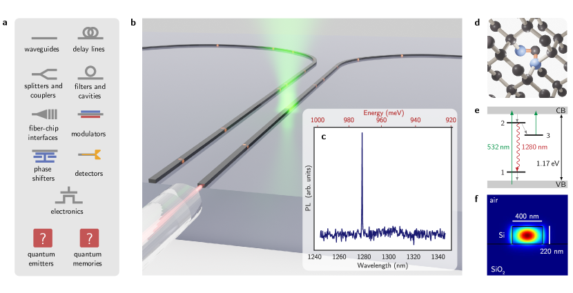
Here we report the first monolithic integration of single artificial atoms – G-centers – in silicon PICs (Fig. 1b) and their optically-induced non-volatile spectral programming. Low temperature spectroscopy reveals single photon emission in the telecommunications O-band (Fig. 1c) with a narrow inhomogeneous distribution of nm and spectral shifts up to 300 pm (55 GHz).
The silicon G-center consists of a pair of substitutional carbon atoms bonded to a silicon self-interstitial (C-Si-C) within the silicon crystal lattice (see Fig 1d). It exhibits a zero phonon line (ZPL) transition at 970 meV (1278 nm), resulting from an electron transition between -like orbitals localized at the Si atom (Fig 1e) and features a spin triplet metastable state Udvarhelyi et al. (2021). While the primary mechanism for above-band population of the excited state in G-centers is likely to be Shockley-Read-Hall (SRH) recombination, additional non-radiative mechanisms such as surface recombination at electronically active surface states and Auger recombination are also known to affect carrier dynamics in silicon Coldren et al. (2012) (a more detailed discussion can be found in SI Section .12).
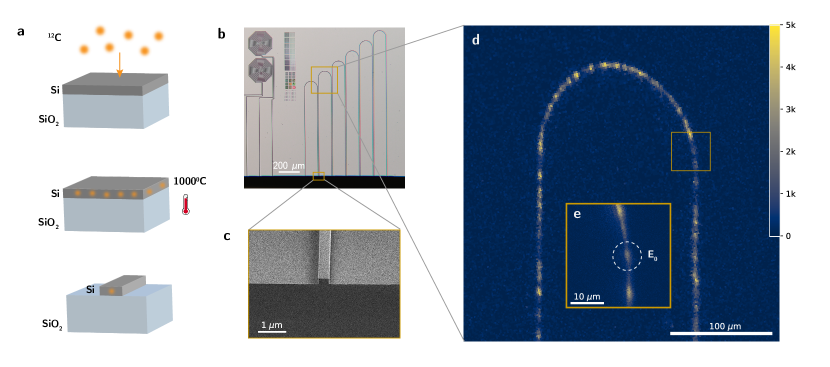
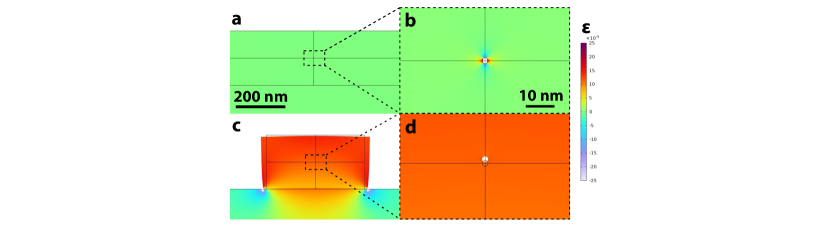
The device under study consists of an SOI waveguide designed for single-mode operation at 1278 nm, the ZPL of the G-center. Simulation results for the electric field distribution within the waveguide are shown in Figure 1f. We fabricated our samples by a combination of commercial carbon implantation, thermal annealing, and foundry electron beam lithography and etching (see Fig. 2a and Methods). Our sample contains several waveguides and photonic structures. The waveguides in our sample (see Fig. 2b) start and end on a cleaved facet (Fig. 2c) and loop in a µm radius bend.
We characterized the samples using low-temperature spectroscopy in a cryostat at a base temperature of K. Using above band-gap laser excitation (wavelength nm, NA=0.55, and power measured before the objective), we induced artificial atoms to emit into the waveguide. The waveguide-coupled optical emission from the emitters was subsequently collected with an edge-coupled lensed fiber at the cleaved chip facet. We band-pass filtered the fiber-collected emission between nm and nm to isolate the zero-phonon line (ZPL) and phonon sideband (PSB) of the G-centers while attenuating residual pump light and other background. The collected emission was then detected with either a cryogenic superconducting-nanowire single-photon detector (SNSPD) system or an infrared spectrometer.
We spatially locate our artificial atoms within the waveguides using photoluminescence (PL) raster scans. We scanned the focused continuous-wave green excitation along the chip plane and detected the filtered emission through the fiber-coupled waveguide with an electronically-gated SNSPD. Figure 2d shows PL signal in spatially-isolated loci along the waveguide, corresponding to single emitters or small ensembles of emitters. A range in brightness of the PL hotspots can be attributed to the presence of clusters of emitters in close proximity, which is confirmed through the observation of multiple distinct ZPL peaks in the PL spectra taken from these points (SI Section .9 and Fig. S5b).
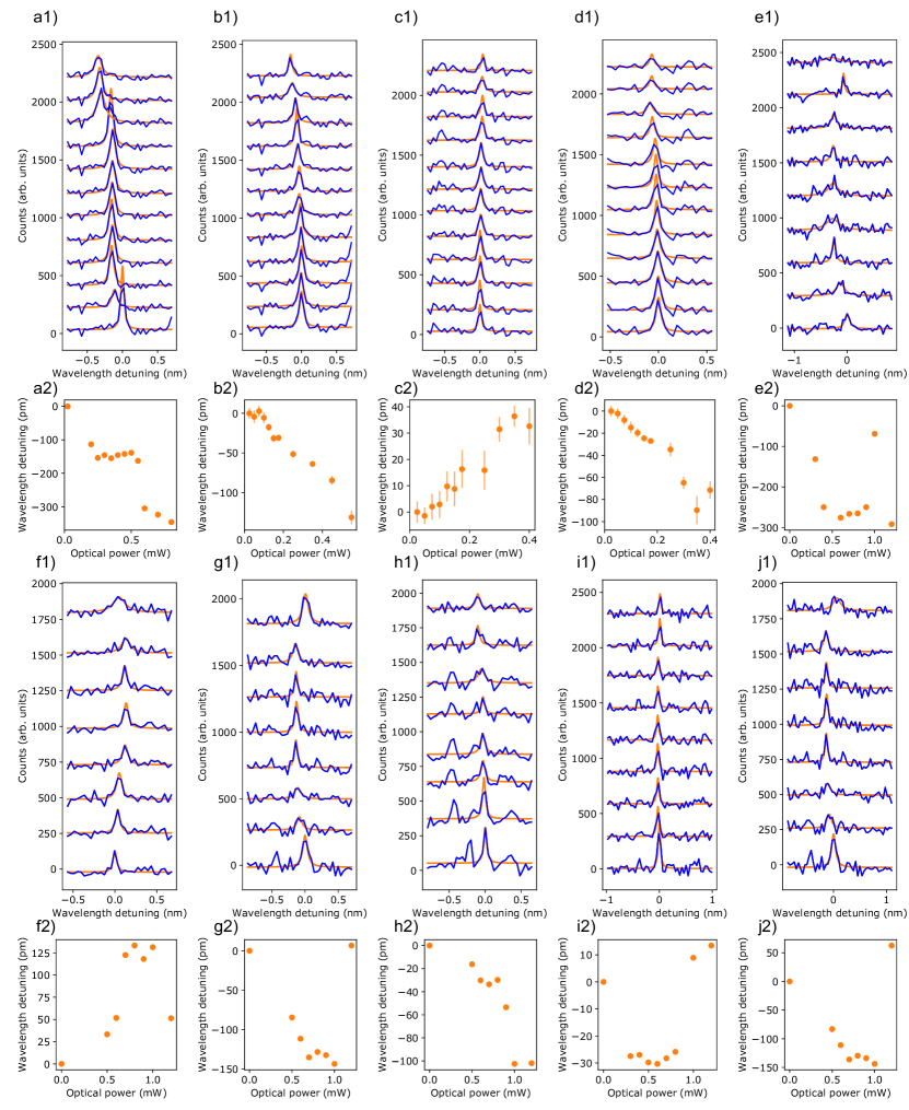
Figure 3a shows that the ZPL distribution of 37 waveguide-coupled G-centers matches a Gaussian probability distribution with a standard deviation of nm, nearly an order of magnitude narrower than previous reports Redjem et al. (2020). Our narrower inhomogeneous distribution may be due to strain relaxation induced by our waveguide geometry (see SI Section .11). The fitted mean ZPL wavelength is nm, in agreement with prior results in bulk SOI Redjem et al. (2020); Beaufils et al. (2018). Using the number and width of the ZPL peaks in the PL spectrum as an indication of the number of individual emitters within each excitation region, we identified locations within the waveguide that are likely to contain single emitters. We isolated one such area, denoted “Emitter 0” (E0, shown in Fig. 2e), and characterized the photophysics of the artificial atom in this region. The PL spectrum from E0 is shown in Fig. 1e and exhibits a single resolution-limited peak at nm. To confirm the presence of a single artificial atom at E0, we performed second-order autocorrelation (Fig. 3b) and power-dependent emission intensity measurements (Fig. 3c).
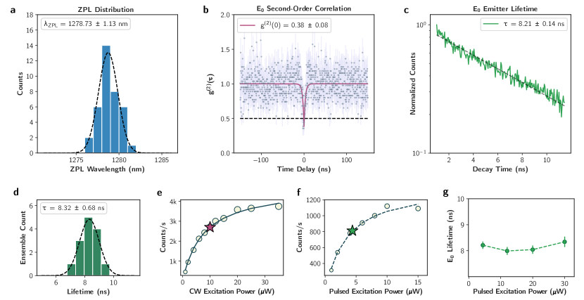
Focusing continuous-wave excitation at 532 nm on E0, we measured the dependence of the emission count rate on the excitation power. In order to distinguish the contribution to the count rate generated by the emitter from the linear fluorescence observed in the waveguide, we performed background subtraction of the count rate (see Methods and SI Section .9). The background-corrected emission fits well to the characteristic two-level emitter saturation model Beaufils et al. (2018), given by
| (1) |
with a saturation power µW, and a saturation intensity under continuous wave (CW) laser excitation of counts per second (Fig. 3e). The extracted saturation power corresponds to an estimated continuous-wave power density of kW, assuming a diffraction-limited spot size with objective NA=0.55. We note, however, that the true excitation area is bounded in one axis by the sub-diffraction waveguide width of 400 nm. These results closely match the saturation power observed for single isolated G-centers in unpatterned SOI wafers Redjem et al. (2020). We performed a similar background-subtracted measurement for 532 nm pulsed excitation (see Methods and SI Section .10 for extended details), resulting in a pulsed saturation average power of µW (Fig. 3f).
Using continuous-wave excitation power of µW (slightly above saturation), we performed second-order autocorrelation measurements using Hanbury-Brown-Twiss interferometry. We split the resulting fiber-collected emission from our sample with a 50:50 O-band fiber beam splitter, followed by detection with two time-tagged SNSPDs (detection efficiencies of 21% and 24% at nm). We fitted the measured histogram of coincidences as a function of time delay between the detection events to the second-order autocorrelation function of a two-level system emitter, displaying an antibunching dip of g (Fig. 3b, see Methods for additional details). The observed antibunching dip with g confirms single-photon emission and individual addressing of a single artificial atom coupled to a silicon photonic waveguide.
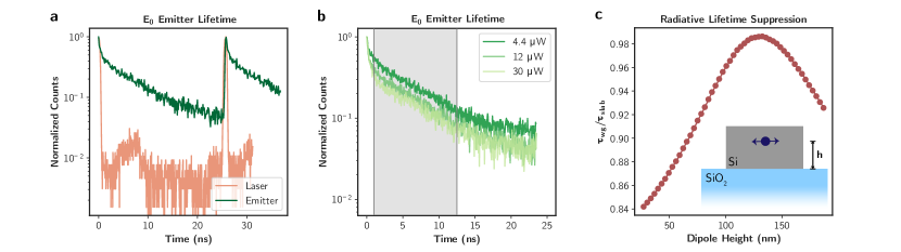
We subsequently measured the excited-state lifetime statistics of emitter E0 and 13 other G-center ensembles (a total of 14 spots) using pulsed 532 nm excitation power of µW, slightly above the measured saturation power for a single emitter. Resulting decay curves fit well to a mono-exponential function, following clipping to remove laser leakage and background (see Methods and SI Section .10). The lifetime distribution of the 14 measured G-center ensembles fits well to a Gaussian distribution with mean lifetime ns and a standard deviation of ns (Fig. 3d). The lifetime of the single G-center at E0 was measured to be ns (Fig. 3c), in close agreement with the mean lifetimes of the measured ensembles. Additionally, we measured the lifetime of the single emitter E0 to be constant over an order of magnitude variation in excitation power (Fig. 3g). Our results agree with previously reported lifetimes in bulk SOI G-center ensembles Beaufils et al. (2018), but indicate shorter lifetimes compared to prior results on isolated G-centers in unpatterned SOI wafers Redjem et al. (2020). Calculations of the dipole local density of optical states (LDOS) in our waveguide were compared to the LDOS of a dipole emitter in a SOI slab (see SI Section .6) and suggest that the reduced lifetime we observe is not explained by field enhancement in the patterning alone. Differences in measured lifetimes in our waveguides could be attributed to increased surface recombination in etched surfaces (see SI Section 6). Other effects affecting the measured lifetimes may be doping and defect density variations between wafers. A quantitative characterization of these effects would include geometry-dependent lifetime measurements, which are out of the scope of this study.
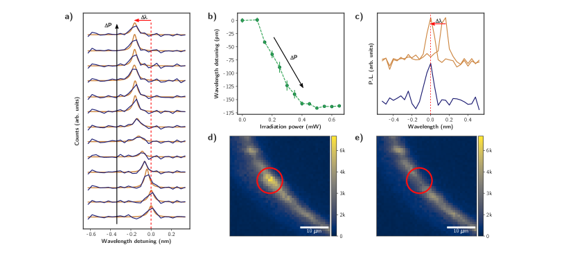
Moreover, we demonstrate non-volatile spectral trimming and deactivation of single color centers in PICs. Our “spectral programming” process consists of in-situ local irradiation of G-centers with a 532 nm CW laser with power above 0.1 mW (estimated power density of kW) during 15 s in our 6 K cryostat, followed by probing PL measurements near emitter saturation powers. Under moderate irradiation powers above 0.1 mW, we observe consistent non-volatile spectral shifts of the ZPL for 11 out of our 12 probed emitters. We observe controllable shifts of average amplitude 150 pm (27.5 GHz) and up to 300 pm (55 GHz) as shown in Fig. 4a and b and Fig. S10), large enough to match the 25 GHz telecommunication bands and to enable spectral alignment of separate emitters (Fig. 4c). Figure S11a and S11b show the spectral stability of our programmed emitters. Higher powers in the order of 1 mW (estimated power density of kW) result in broadening and deactivation of the emitter, leaving the waveguide and adjacent emitters unaffected (Fig. 4d and e and the subtracted PL map in Fig. S12). In our experiments, the programming and deactivation effects are non-reversible. Given that our simulations rule out local annealing as a cause for the trimming and deactivation effects (see SI Section .14), we hypothesize that these effects are caused by optically-induced variation of surface charges leading to Stark tuning of the emitters, followed by ionization into the dark A state Udvarhelyi et al. (2021) for high charge densities. For more information on the process, results, and our hypotheses on the physics behind this effect, see SI Section .14.
The count rates in our waveguide measurements were limited by preventable loss due to imperfect mode matching between our cleaved waveguide facet and the lensed collection fiber. A mode overlap simulation between the SOI waveguide and fiber mode predicts an upper bound on the coupling efficiency in our system to be % (see SI Section .6). In practice, this excess loss restricts our excitation to a small range near the saturation power of the emitter, as the signal-to-noise ratio of the emission decreases at low excitation powers due to the detector dark counts and also at high excitation powers due to the background fluorescence (see SI Section .9). This low signal to noise ratio is the reason behind our non-zero g. However, the coupling efficiency can be easily improved by up to an order of magnitude using widely available photonic components such as spot-size converters or grating couplers, that can achieve coupling efficiencies in excess of % Zhang et al. (2020); Chen et al. (2017).
Another notable difference between our waveguide-integrated G-centers compared to those measured in unpatterned SOI wafers concerns the position of observed emitters selected by the collection mode. Solid-state emitters often show decreased spectral stability in proximity to surfaces due to emitter-surface interactions Chakravarthi et al. (2021). Simulations of dipole collection efficiency as a function of dipole depth within our waveguides suggest that we preferentially observe emission from G-centers near the center of the silicon film (SI Section .6, Fig. S2b). On the other hand, prior results using confocal collection of G-center emission from silicon slabs select for emitters close to the surface Redjem et al. (2020). This geometrical filtering effect may also explain the absence in our measurements of other emitters previously observed in silicon Durand et al. (2021), or those created by etching processes. Our measurements show high emission stability down to a 10 ms timescale for a range of excitation powers, as well as robustness to photobleaching, enabling emission measurements over time intervals greater than one month (see SI Section .13). A comparative study looking into G-center emission at varying depths would required to probe the emitter-surface interaction for these artificial atoms, but this falls out of the scope of this work.
Our in-situ non-volatile trimming results show a path towards post-fabrication fine tuning of artificial atoms. Such an effect is large enough to tune emitters into standard 25 GHz telecommunication bands, to align emitters to cavities and enhance light-matter interaction, or to spectrally align separate emitters and achieve quantum interference or cooperative emission. In addition, the local deactivation of emitters presented here can aid in trimming waveguides and cavities of unwanted artificial atoms. Further work is required to reveal the physics behind the observed effect and potentially increase its range. This may involve performing higher resolution spectroscopy, measuring samples with different geometries and crystal purity, experimenting with pulsed lasers and other wavelengths, performing in-situ temperature measurements, measuring its dynamics, or searching for correlations between trimming performance and dipole orientation.
Efficient integration with PICs is a key requirement for any large-scale artificial atom qubit platform. Therefore, the results presented here characterizing single G-center emission and trimming in silicon-on-insulator waveguides provide a key step forward for quantum information processing based on color centers in silicon. Moreover, our use of a commercial foundry for the fabrication process makes our results scalable and inherently repeatable by the scientific community, without the need to re-develop an in-house fabrication process. Promising future research directions include the Purcell-enhanced emission from single G-centers in resonant structures and the generation of spectrally indistinguishable single photons for quantum interference using optical trimming, electric fields Anderson et al. (2019), or mechanical strain Wan et al. (2020). As demonstrated in other color centers Bhaskar et al. (2020), coupling emitters into cavities help overcome low quantum efficiencies and Debye-Waller factors. This may not only aid in the development of spin-optic interfaces, but also may enable deterministic single-photon emission and photon-photon interactions via cavity quantum electrodynamics Janitz et al. (2020). Investigation of the spin properties of the G-center metastable state Udvarhelyi et al. (2021), particularly its spin lifetime, and the 13C and 29Si nuclear degrees of freedom Wolfowicz et al. (2016) could additionally enable optically-active quantum memories hosted in silicon photonics. Finally, our results also motivate the study and waveguide integration of other radiation damage centers in silicon, such as the recently isolated T-center Bergeron et al. (2020) and W-center Baron et al. (2021).
In conclusion, we demonstrated individually addressable artificial atoms operating at telecommunication wavelengths and featuring narrow inhomogeneous distributions in a foundry-written silicon photonic circuit, as well as a new method to spectrally program them and deactivate them using light. Our results show native and spectrally programmable single-photon emission and pave the way towards spin qubits in silicon waveguides, establishing silicon photonics as a promising platform for large-scale quantum information technologies.
II Methods
II.1 Sample description
The device under study consists of a background p-doped silicon-on-insulator waveguide with µm silicon dioxide bottom cladding on a silicon substrate. The cross-sectional geometry is shown in Fig. 1f and is rectangular with nm width and nm height. The waveguide starts and ends on a cleaved chip facet and loops in a µm radius bend.
II.2 Sample fabrication
We generated silicon G-centers using a fabrication process that follows Redjem et al. (2020). The samples started from a commercial (SOITEC) unclad silicon-on-insulator wafer ( nm Si on nm SiO2). The wafer was then cleaved into cm2 pieces, implanted with 12C with a dose of ions/cm-2 at keV energy and at an angle of , and then flash annealed for s at C. The sample was then electron-beam patterned and etched in a foundry (Applied Nano Tools). The silicon etching was performed using inductively coupled plasma reactive ion etching with SF6-C4F8 mixed-gas, in a process optimized for vertical sidewall etching and low propagation loss. This process resulted in silicon waveguides with SiO2 bottom cladding and air as top cladding. To enable fiber coupling, the sample was cleaved across the waveguides.
II.3 Photophysics characterization
Optical excitation of the G-centers was performed through the cryostat window using long working distance objectives with numerical aperture of . Waveguide-coupled emission was collected from a single waveguide output using a SMF-28 lensed fiber and spectrally filtered in free space to select signal between and nm. The signal was then detected using either time-tagged SNSPD or an infrared spectrometer with a wavelength resolution of 155 pm. We measured the excitation powers for all presented measurements immediately prior to the microscope objective.
Photoluminescence (PL) raster scans were acquired by scanning the focused excitation spot over a spatial region of the waveguide sample and gating the SNSPD integration with the electronic trigger of the scanning mirrors. Background-corrected PL spectra were then measured using the infrared spectrometer, where the background spectrum recorded environmental light conditions with the laser blocked.
Saturation curves were measured at a spatial location in the waveguide that exhibited bright PL intensity and a ZPL peak near the 1280 nm transition of the G-center. Correction of the count rate due to the waveguide background was performed prior to fitting with the saturation model in Eq. (1) (see SI Section .9 for details on background measurements and subtraction).
The second-order correlation (g) was measured with continuous-wave 532 nm excitation near the saturation power. Emission from the waveguide was split with a 50:50 O-band fiber beamsplitter prior to time-tagged detection by DET1 and DET2. A histogram of the coincidences as a function of time difference between detector clicks was acquired with 300 ps binwidth and fitted to the second order correlation of a two-level system Redjem et al. (2020):
| (2) |
The resulting second-order correlation of g indicates single-photon emission. Poissonian error bars were applied to the data points in Fig. 3b. The error bar on g refers to the error of the fit calculated from the covariance in Python’s scipy.curve_fit() function.
Emitter decay lifetimes were measured using pulsed 532 nm excitation at a repetition rate of 34 MHz. A histogram of the SNSPD clicks as a function of the delay time between the detection event and the pulsed laser trigger were first clipped to remove laser leakage and background (see SI Fig. S6a-b for details). The resulting decay curves fit well to a mono-exponential function:
| (3) |
with an emitter lifetime of ns. Here, the error bar on the lifetime of a single emitter is again calculated from the error of the fit.
II.4 System efficiency
The collection efficiency of our system was characterized as follows:
-
•
: Simulated edge coupling efficiency between the cleaved waveguide mode and a perfectly aligned lensed fiber was simulated to be at 1280 nm.
-
•
: Maximum dipole coupling to a uni-directional waveguide mode was simulated to be (see SI Fig. S2a-b for details).
-
•
: Free space fiber filtering with two fiber collimators was measured to have transmission at 1280 nm.
-
•
: Fiber routing to the two SNSPD cryostat detectors DET1 and DET2 was measured to be and , respectively.
-
•
: Insertion loss of fiber beamsplitter was measured to be .
-
•
: SNSPD detector efficiencies at 1280 nm for DET1 and DET2 were characterized to be and , respectively. These SNSPDs were manufactured to have high efficiency at a target wavelength of 1550 nm.
The total system efficiency, given by
| (4) |
can, therefore, be upper bounded to for DET1 and for DET2. Using the above estimates for the collection efficiency and an observed saturated count rate of 138259 counts/second under 78 MHz pulsed excitation, we estimate a lower bound on the quantum efficiency of . However, the uncertainty on this estimate is large, due to low measured count rates and estimates of and being derived from simulation.
Acknowledgements
The authors would like to acknowledge Dr. Matt Trusheim and Isaac Harris for useful discussions regarding emission physics and defect structure. The authors would also like to thank Dr. Dalia Ornelas-Huerta for contributions to the experimental setup.
M.P. acknowledges funding from the National Science Foundation (NSF) Convergence Accelerator Program under grant No.OIA-2040695 and Harvard MURI under grant No.W911NF-15-1-0548. C.E-H. and L.D. acknowledge funding from the European Union’s Horizon 2020 research and innovation program under the Marie Sklodowska-Curie grant agreements No.896401 and 840393. I.C. acknowledges funding from the National Defense Science and Engineering Graduate (NDSEG) Fellowship Program and NSF award DMR-1747426. D.E. acknowledges support from the NSF RAISE TAQS program. This material is based on research sponsored by the Air Force Research Laboratory (AFRL), under agreement number FA8750-20-2-1007. The U.S. Government is authorized to reproduce and distribute reprints for Governmental purposes notwithstanding any copyright notation thereon. The views and conclusions contained herein are those of the authors and should not be interpreted as necessarily representing the official policies or endorsements, either expressed or implied, of the Air Force Research Laboratory (AFRL), or the U.S. Government.
Data availability
The datasets generated and analysed during this study are available from the corresponding authors on reasonable request.
References
- Ruf et al. (2021) M. Ruf, N. H. Wan, H. Choi, D. Englund, and R. Hanson, Journal of Applied Physics 130, 070901 (2021).
- Bhaskar et al. (2020) M. K. Bhaskar, R. Riedinger, B. Machielse, D. S. Levonian, C. T. Nguyen, E. N. Knall, H. Park, D. Englund, M. Lončar, D. D. Sukachev, and M. D. Lukin, Nature 580, 60 (2020).
- Atatüre et al. (2018) M. Atatüre, D. Englund, N. Vamivakas, S.-Y. Lee, and J. Wrachtrup, Nature Reviews Materials 3, 38 (2018).
- Aharonovich et al. (2016) I. Aharonovich, D. Englund, and M. Toth, Nature Photonics 10, 631 (2016).
- Degen et al. (2017) C. L. Degen, F. Reinhard, and P. Cappellaro, Reviews of Modern Physics 89, 035002 (2017).
- Childress and Hanson (2013) L. Childress and R. Hanson, MRS Bulletin 38, 134 (2013).
- Choi et al. (2019) H. Choi, M. Pant, S. Guha, and D. Englund, npj Quantum Information 5, 1 (2019).
- Bergeron et al. (2020) L. Bergeron, C. Chartrand, A. T. K. Kurkjian, K. J. Morse, H. Riemann, N. V. Abrosimov, P. Becker, H.-J. Pohl, M. L. W. Thewalt, and S. Simmons, PRX Quantum 1, 020301 (2020).
- Baron et al. (2021) Y. Baron, A. Durand, P. Udvarhelyi, T. Herzig, M. Khoury, S. Pezzagna, J. Meijer, I. Robert-Philip, M. Abbarchi, J.-M. Hartmann, V. Mazzocchi, J.-M. Gérard, A. Gali, V. Jacques, G. Cassabois, and A. Dréau, arXiv:2108.04283 [physics, physics:quant-ph] (2021), arXiv:2108.04283 [physics, physics:quant-ph] .
- Durand et al. (2021) A. Durand, Y. Baron, W. Redjem, T. Herzig, A. Benali, S. Pezzagna, J. Meijer, A. Y. Kuznetsov, J.-M. Gérard, I. Robert-Philip, M. Abbarchi, V. Jacques, G. Cassabois, and A. Dréau, Physical Review Letters 126, 083602 (2021).
- Higginbottom et al. (2022) D. B. Higginbottom, A. T. K. Kurkjian, C. Chartrand, M. Kazemi, N. A. Brunelle, E. R. MacQuarrie, J. R. Klein, N. R. Lee-Hone, J. Stacho, M. Ruether, C. Bowness, L. Bergeron, A. DeAbreu, S. R. Harrigan, J. Kanaganayagam, D. W. Marsden, T. S. Richards, L. A. Stott, S. Roorda, K. J. Morse, M. L. W. Thewalt, and S. Simmons, Nature 607, 266 (2022).
- Hollenbach et al. (2020) M. Hollenbach, Y. Berencén, U. Kentsch, M. Helm, and G. V. Astakhov, Optics Express 28, 26111 (2020).
- Redjem et al. (2020) W. Redjem, A. Durand, T. Herzig, A. Benali, S. Pezzagna, J. Meijer, A. Y. Kuznetsov, H. S. Nguyen, S. Cueff, J.-M. Gérard, I. Robert-Philip, B. Gil, D. Caliste, P. Pochet, M. Abbarchi, V. Jacques, A. Dréau, and G. Cassabois, Nature Electronics 3, 738 (2020).
- Wan et al. (2020) N. H. Wan, T.-J. Lu, K. C. Chen, M. P. Walsh, M. E. Trusheim, L. De Santis, E. A. Bersin, I. B. Harris, S. L. Mouradian, I. R. Christen, E. S. Bielejec, and D. Englund, Nature 583, 226 (2020).
- Wolfowicz et al. (2020) G. Wolfowicz, C. P. Anderson, B. Diler, O. G. Poluektov, F. J. Heremans, and D. D. Awschalom, Science Advances 6, eaaz1192 (2020).
- Kim et al. (2020) J.-H. Kim, S. Aghaeimeibodi, J. Carolan, D. Englund, and E. Waks, Optica 7, 291 (2020).
- Elshaari et al. (2020) A. W. Elshaari, W. Pernice, K. Srinivasan, O. Benson, and V. Zwiller, Nature Photonics 14, 285 (2020).
- Dréau et al. (2018) A. Dréau, A. Tchebotareva, A. E. Mahdaoui, C. Bonato, and R. Hanson, Physical Review Applied 9, 064031 (2018).
- Tyryshkin et al. (2012) A. M. Tyryshkin, S. Tojo, J. J. L. Morton, H. Riemann, N. V. Abrosimov, P. Becker, H.-J. Pohl, T. Schenkel, M. L. W. Thewalt, K. M. Itoh, and S. A. Lyon, Nature Materials 11, 143 (2012).
- Saeedi et al. (2013) K. Saeedi, S. Simmons, J. Z. Salvail, P. Dluhy, H. Riemann, N. V. Abrosimov, P. Becker, H.-J. Pohl, J. J. L. Morton, and M. L. W. Thewalt, Science 342, 830 (2013).
- Plummer et al. (2000) J. D. Plummer, M. Deal, and P. B. Griffin, Silicon VLSI Technology: Fundamentals, Practice and Modeling (Prentice Hall, Upper Saddle River, NJ, USA, 2000).
- Yeap et al. (2019) G. Yeap, S. S. Lin, Y. M. Chen, H. L. Shang, P. W. Wang, H. C. Lin, Y. C. Peng, J. Y. Sheu, M. Wang, X. Chen, B. R. Yang, C. P. Lin, F. C. Yang, Y. K. Leung, D. W. Lin, C. P. Chen, K. F. Yu, D. H. Chen, C. Y. Chang, H. K. Chen, P. Hung, C. S. Hou, Y. K. Cheng, J. Chang, L. Yuan, C. K. Lin, C. C. Chen, Y. C. Yeo, M. H. Tsai, H. T. Lin, C. O. Chui, K. B. Huang, W. Chang, H. J. Lin, K. W. Chen, R. Chen, S. H. Sun, Q. Fu, H. T. Yang, H. T. Chiang, C. C. Yeh, T. L. Lee, C. H. Wang, S. L. Shue, C. W. Wu, R. Lu, W. R. Lin, J. Wu, F. Lai, Y. H. Wu, B. Z. Tien, Y. C. Huang, L. C. Lu, J. He, Y. Ku, J. Lin, M. Cao, T. S. Chang, and S. M. Jang, in 2019 IEEE International Electron Devices Meeting (IEDM) (2019) pp. 36.7.1–36.7.4.
- Vivien and Pavesi (2016) L. Vivien and L. Pavesi, Handbook of Silicon Photonics (CRC Press, Boca Raton, FL, USA, 2016).
- Panuski et al. (2020) C. Panuski, D. Englund, and R. Hamerly, Physical Review X 10, 041046 (2020).
- Chakraborty et al. (2020) U. Chakraborty, J. Carolan, G. Clark, D. Bunandar, G. Gilbert, J. Notaros, M. R. Watts, and D. R. Englund, Optica 7, 1385 (2020).
- Edinger et al. (2021) P. Edinger, A. Y. Takabayashi, C. Errando-Herranz, U. Khan, H. Sattari, P. Verheyen, W. Bogaerts, N. Quack, and K. B. Gylfason, Optics Letters 46, 5671 (2021).
- Gyger et al. (2021) S. Gyger, J. Zichi, L. Schweickert, A. W. Elshaari, S. Steinhauer, S. F. Covre da Silva, A. Rastelli, V. Zwiller, K. D. Jöns, and C. Errando-Herranz, Nature Communications 12, 1408 (2021).
- Pernice et al. (2012) W. H. P. Pernice, C. Schuck, O. Minaeva, M. Li, G. N. Goltsman, A. V. Sergienko, and H. X. Tang, Nature Communications 3, 1325 (2012).
- Giewont et al. (2019) K. Giewont, K. Nummy, F. A. Anderson, J. Ayala, T. Barwicz, Y. Bian, K. K. Dezfulian, D. M. Gill, T. Houghton, S. Hu, B. Peng, M. Rakowski, S. Rauch, J. C. Rosenberg, A. Sahin, I. Stobert, and A. Stricker, IEEE Journal of Selected Topics in Quantum Electronics 25, 1 (2019).
- Tait et al. (2020) A. N. Tait, S. M. Buckley, J. Chiles, A. N. McCaughan, S. Olson, S. P. Rao, S. W. Nam, R. P. Mirin, and J. M. Shainline, Journal of Physics: Photonics 2, 045001 (2020).
- Buckley et al. (2020) S. M. Buckley, A. N. Tait, G. Moody, B. Primavera, S. Olson, J. Herman, K. L. Silverman, S. P. Rao, S. W. Nam, R. P. Mirin, and J. M. Shainline, Optics Express 28, 16057 (2020).
- Lodahl et al. (2015) P. Lodahl, S. Mahmoodian, and S. Stobbe, Reviews of Modern Physics 87, 347 (2015).
- Udvarhelyi et al. (2021) P. Udvarhelyi, B. Somogyi, G. Thiering, and A. Gali, Physical Review Letters 127, 196402 (2021).
- Coldren et al. (2012) L. A. Coldren, S. W. Corzine, and M. L. Mashanovitch, Diode Lasers and Photonic Integrated Circuits, 2nd ed. (Wiley, Hoboken, NJ, USA, 2012).
- Beaufils et al. (2018) C. Beaufils, W. Redjem, E. Rousseau, V. Jacques, A. Y. Kuznetsov, C. Raynaud, C. Voisin, A. Benali, T. Herzig, S. Pezzagna, J. Meijer, M. Abbarchi, and G. Cassabois, Physical Review B 97, 035303 (2018).
- Zhang et al. (2020) X. Zhang, B. Chen, Z. Ruan, W. Liu, P. Chen, Y. Shi, and L. Liu, Optics Communications 465, 125554 (2020).
- Chen et al. (2017) X. Chen, D. J. Thomson, L. Crudginton, A. Z. Khokhar, and G. T. Reed, Optics Express 25, 17864 (2017).
- Chakravarthi et al. (2021) S. Chakravarthi, C. Pederson, Z. Kazi, A. Ivanov, and K.-M. C. Fu, Physical Review B 104, 085425 (2021).
- Anderson et al. (2019) C. P. Anderson, A. Bourassa, K. C. Miao, G. Wolfowicz, P. J. Mintun, A. L. Crook, H. Abe, J. Ul Hassan, N. T. Son, T. Ohshima, and D. D. Awschalom, Science 366, 1225 (2019).
- Janitz et al. (2020) E. Janitz, M. K. Bhaskar, and L. Childress, Optica 7, 1232 (2020).
- Wolfowicz et al. (2016) G. Wolfowicz, P.-A. Mortemousque, R. Guichard, S. Simmons, M. L. W. Thewalt, K. M. Itoh, and J. J. L. Morton, New Journal of Physics 18, 023021 (2016).
- Baron et al. (2022) Y. Baron, A. Durand, T. Herzig, M. Khoury, S. Pezzagna, J. Meijer, I. Robert-Philip, M. Abbarchi, J.-M. Hartmann, S. Reboh, J.-M. Gérard, V. Jacques, G. Cassabois, and A. Dréau, Applied Physics Letters 121, 084003 (2022).
- Green (2008) M. A. Green, Solar Energy Materials and Solar Cells 92, 1305 (2008).
- Degallaix et al. (2014) J. Degallaix, J. Komma, D. Forest, G. Hofmann, M. Granata, D. Heinert, C. Schwarz, R. Nawrodt, L. Pinard, C. Michel, R. Flaminio, and G. Cagnoli, Classical and Quantum Gravity 31, 185010 (2014).
- Asheghi et al. (1998) M. Asheghi, M. N. Touzelbaev, K. E. Goodson, Y. K. Leung, and S. S. Wong, Journal of Heat Transfer 120, 30 (1998).
- Glassbrenner and Slack (1964) C. J. Glassbrenner and G. A. Slack, Phys. Rev. 134, A1058 (1964).
- Bassett et al. (2011) L. C. Bassett, F. J. Heremans, C. G. Yale, B. B. Buckley, and D. D. Awschalom, Physical Review Letters 107, 266403 (2011).
- Strand et al. (2018) J. Strand, M. Kaviani, D. Gao, A.-M. El-Sayed, V. V. Afanas’ev, and A. L. Shluger, Journal of Physics: Condensed Matter 30, 233001 (2018).
- Afanas’ev and Adamchuk (1994) V. V. Afanas’ev and V. K. Adamchuk, Progress in Surface Science 47, 301 (1994).
- Aslam et al. (2013) N. Aslam, G. Waldherr, P. Neumann, F. Jelezko, and J. Wrachtrup, New Journal of Physics 15, 013064 (2013).
- Lee et al. (1982) K. M. Lee, K. P. O’Donnell, J. Weber, B. C. Cavenett, and G. D. Watkins, Physical Review Letters 48, 37 (1982).
Supplementary Information
.5 Measurement setup
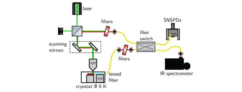
Figure S1 shows the measurement setup we used in this work. Description of the components of the measurement apparatus pertaining to the optical characterization of emitters is presented in the Methods section of the main text. We include additional setup details in this section for completeness. Our continuous wave excitation source is a Coherent Verdi G5 at 532 nm, and our pulsed excitation is an NKT Photonics SuperK laser with a maximum repetition rate of 78 MHz and a pulse length below 1 ns. To avoid background from our laser, the excitation path was filtered with a nm band-pass filter (Semrock Maxline bandpass with 2 nm FWHM). Our microscope objective is a Mitutoyo M Plan APO and Mitutoyo M Plan APO SL.
Our cryostat is a Montana Instruments CR-057 with a home-made fiber feedthrough. The fiber we use (OZ Optics, spot size of 2.5 µm at 1550 nm, and expected spot size of 2.1 µm at 1300 nm) is mounted on a XYZ cryogenic piezoelectric stage (Attocube). Our free-space filtering setup consists of a 1250 nm longpass (Thorlabs FEL1250) and a 1550 nm shortpass (Edmund Optics OD2) filters. To detect our PL we use two superconducting nanowire single photon detectors (NIST) with detection efficiencies and and timing jitters below and ps, readout with a Swabian Instruments Timetagger 20. Alternatively, we use a IR spectrometer consisting of a PyLon IR InGaAs linear CCD array from Princeton Instruments and two gratings with densities of 300 g/mm and 900 g/mm, 1.2 µm and 1.3 µm blazes, and resulting resolutions of 155 pm and 40 pm respectively. For the second order autocorrelation measurement we used a fiber beam splitter (Thorlabs TW1300R5F1) after the filtering station.
.6 Coupling efficiency simulations between emitter, waveguide, and fiber
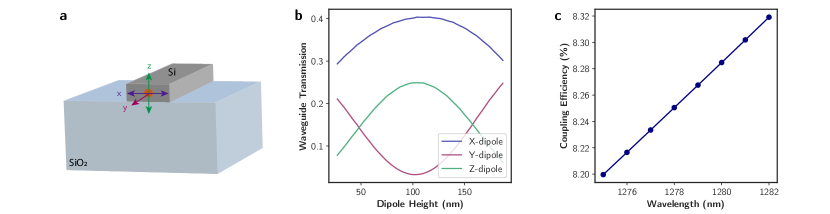
Finite difference time domain (Lumerical FDTD) simulations were performed to calculate the emitter-waveguide coupling as a function of the emitter height in the waveguide. Directional waveguide-coupled dipole emission was measured using a power monitor at one end of the waveguide, with a dipole emitter oriented in either the X-, Y-, or Z-direction positioned at a range of heights within the waveguide (Fig. S2a). The single-ended waveguide transmission for each direction and dipole height is shown in Fig. S2b. We observe an improved waveguide coupling for dipoles oriented transverse to the waveguide axis and near the center of the silicon film. Our asymmetric waveguide geometry preferentially supports quasi-TE modes over quasi-TM, so the improved coupling for the dipoles oriented along the long transverse axis of the waveguide agrees with expectations. We note that the waveguide collection could be improved by up to a factor of two by adding a reflector at the other end of the waveguide.
The edge coupling efficiency between the cleaved waveguide mode (shown in Fig 1f) and a perfectly aligned lensed fiber was simulated using Lumerical MODE Solutions eigenmode solver. We simulated the mode at the focus spot of the fiber as a Gaussian beam with 2.1 µm diameter, and the waveguide mode as the output of a waveguide mode eigenmode simulation. Our mode overlap calculations, including the Fresnel reflection at the waveguide-air interface, yield the coupling efficiency in Fig. S2c, and a efficiency at 1280 nm.
.7 Confocal collection from vertically-coupled structures
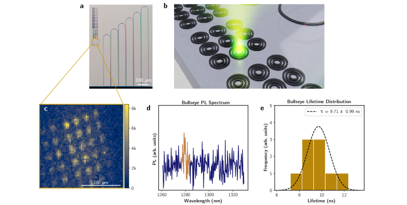
In addition to waveguides, the fabricated G-center sample consists of bulls-eye grating structures, designed for a vertically-coupled cavity mode near 1275 nm (Fig. S3a-b) with . The objective used for both excitation and collection was a Mitutoyo M Plan APO long working distance objective (NA=0.55). It is worth noting that the specified objective has an designed operating range of 435-655 nm, which is optimized for transmission of the 532 nm excitation path. However, confocal collection around 1280 nm falls outside this range. Raster scans of the vertically-coupled PL signal were acquired in the same way as the through-waveguide measurements. Distinct PL intensity maxima are observed over the bulls-eye structures (Fig. S3c); however, the observed count rates were much lower for the same excitation power than with through-waveguide emission. A background-corrected PL spectrum from one of these structures was collected with the maximum spectrometer integration time of 800 seconds. A dim peak at 1278.622 nm was observed (Fig. S3d), suggesting the presence of the G-centers in these structures. Lifetimes for 9 of these structures were measured, using the same protocol for fitting as the waveguide samples. The distribution of the lifetimes in the bulls-eyes was observed to be ns, slightly higher than those observed for G-centers in waveguides.
.8 Ion implantation simulations
The carbon ion implantation depth was simulated using Stopping and Range of Ions in Matter (SRIM).The simulated layer was 220 nm of 28Si with a density of g/cm3, and the simulated ions were 12C with an acceleration of 36 keV and incident at an angle of . The simulation results, shown in Fig. S4 yield an ion range (i.e. mean ion depth) of nm with a straggle (i.e. standard deviation) of nm, a skewness of -0.259 and a Kurtosis of 2.6411.

.9 Background correction for saturation
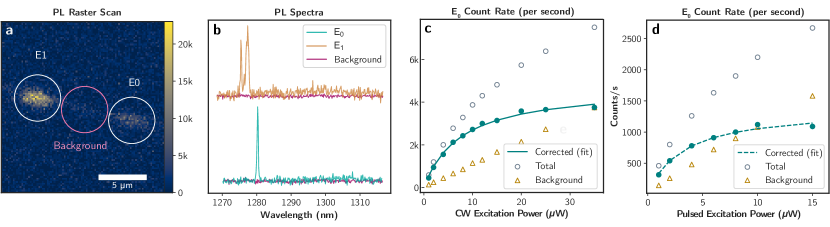
A PL signal was observed in the waveguide regions between PL maxima, particularly at high excitation powers. As a result, a protocol to measure and subtract this background was necessary to separate the count rate from the emitters from the background counts generated in the waveguide. First, PL maps were taken to isolate points that contain G-centers, as well as to locate a point in the waveguide to measure the background. The regions isolated for this measurement are shown in Fig. S5a. The spectra of the PL signal from the two emitter points, E0 and E1 show ZPL peaks near 1280 nm, whereas the background waveguide region shows no ZPL emission (Fig. S5b). The count rate at the single emitter spot E0 and the background region was measured over a range of excitation powers. The background-corrected emitter saturation was calculated by subtracting the total count rate at the emitter from the counts measured in the waveguide background region. Figures S5c-d show the results of the background correction for both CW and pulsed 532 nm excitation.
.10 Lifetime fitting
The emitter lifetimes were measured using 532nm pulsed excitation from the SuperK laser. A repetition rate of 34 MHz was selected to enable decay curves of up to 29 ns to be acquired. The resulting raw decay curves exhibit both an initial peak at the onset of the pulse, as well as flattening towards the end of the pulse period from count background. Fig. S6a shows a plot of the normalized emitter lifetime compared to the normalized lifetime of the pulsed laser. A bi-exponential fit of the raw lifetime data confirms that the time constant of the initial peak matches with that of the excitation laser. Additionally, it can be seen in Fig. S6b that increasing the excitation power does not change the lifetime slope; however, the fractional contribution of the initial peak to the total counts increases with higher laser power. Furthermore, it is observed that the decay becomes background-limited near 15 ns post-excitation. The final lifetime is calculated by clipping the raw lifetime to a range between 1 ns and 12.5 ns before fitting to a single exponential function (Fig. S6b).
We compared our simulations of the local density of optical states (LDOS) for a dipole emitter in our waveguide (400 nm 220 nm) to those of the dipole LDOS in a 220 nm thick slab SOI to estimate the change in the radiative lifetime of our patterned sample. The dipole radiation power was simulated in Lumerical FDTD along the three cardinal axes to calculate the total LDOS for an emitter with a random orientation within the waveguide. A similar simulation was calculated for dipoles placed in a slab SOI. The radiative lifetime, , is inversely proportional to the LDOS, , so the suppression in radiative lifetime in the waveguide compared to a slab is
| (5) |
and was calculated over a range of possible dipole heights within the waveguide (Fig. S6c). From this simulation, we observe that the change in radiative lifetime due to waveguide patterning of a slab does not fully explain the difference observed between our results and that of isolated single G-centers in SOI slabs Redjem et al. (2020).
.11 Simulations of strain distribution in SOI waveguides and slabs
It is well known that commercial SOI wafers have significant intrinsic stress. The presence of a defect in the lattice induces stress relaxation into strain gradients localized around the defect, which may result in a significant inhomogeneous ditribution for a constrained SOI slab, such as for the results presented in Redjem et al. (2020). In contrast, for the more mechanically compliant case of a patterned waveguide, the stress in the film relaxes largely into homogeneous strain (i.e. by deforming the waveguide cross-section), potentially resulting in a narrower inhomogeneous distribution.
We qualitatively modeled this effect by assuming a nanoscale air defect (simulated as an air gap of 1 nm radius) in a isotropic silicon film. Using COMSOL Multiphysics v5.5, we simulated a 2D silicon slab with fully clamped sidewalls and our defect under the 38 MPa biaxial (x-axis in the simulation) compressive stress reported for photonic SOI.The resulting strain distribution is shown in Fig. S7a and b, and shows height-independent volumetric strain gradients in the order of in the vicinity of the defect. In contrast, the simulation results for a 400 nm wide waveguide in Fig. S7c and d show reduced strain gradients for all defect positions () and an order of magnitude () in the center of the waveguide.
Although these results do not quantitatively model a real defect in a solid, they provide a qualitative intuition for a possible explanation to our observation of a reduced inhomogeneous distribution in waveguides.
.12 Defect-related carrier dynamics
The photodynamics of the G-center emission under above-bandgap excitation is described here with the rate equation model depicted in Fig. S8. As silicon possesses an indirect bandgap at a transition near nm (1.17 eV), we assume that the band-to-band radiative recombination rate is negligible. The primary mechanisms governing carrier dynamics in silicon are Shockley-Read-Hall (SRH) trap recombination, surface recombination, and Auger recombination Coldren et al. (2012). The waveguide devices presented in this paper do not have a top oxide cladding and are not passivated to reduce surface trap states; therefore, we expect a non-negligible recombination from surface effects at the waveguide sidewalls. The main pathway to populate the excited state of the G-center is determined by the rate , which is an effective rate including the influence of trap states in the silicon. Once populated, the emission dynamics from the G-centers is following the behaviour of a 2 level system with an additional shelving state.
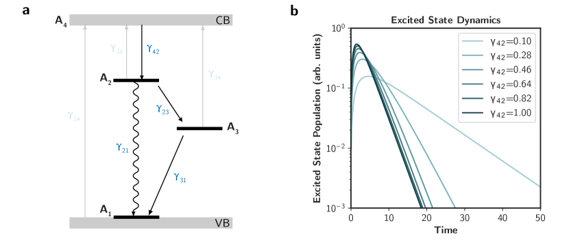
The dynamics of this system are described by the following rate equations, where corresponds to the carrier occupation density at level .
| (6) |
The transition rates from state Ai to state Aj depend on a number of material properties in the patterned silicon structures, and as such, the calculation of the exact rates is out the scope of this study. The level occupation densities can be obtained using a matrix exponential solution to the system of coupled differential equations. Due to the coupled nature of the rate equations, the time-dependent state occupations depend on contributions from each of the rate terms, determined by the eigenvalues of the coefficient matrix in Eqn. (6). The assumptions and general physical mechanisms that can govern these rates are described below:
-
•
: denotes the electron pumping rate, under the assumption that the conduction band occupation is much lower than the valence band occupation (). Our lifetime measurements are performed under pulsed excitation, so we assume pumping and re-pumping processes (including and ) to the conduction band to be zero after the initial pulse.
-
•
: the rate of thermalized excitation of electrons from the upper defect level to the conduction band (a function of material doping and temperature, ), which includes a re-pumping term (set to zero after the pulse, see above).
-
•
: the rate of electron capture from the conduction band to the upper trap state depends on material properties of the wafer and structures, including the electron capture cross-section, ; the density of surface traps, ; and the carrier density, .
-
•
: describes effective radiative emission rate from the defect excited state to ground state in the presence of a perturbed local density of optical states (LDOS), where enhancement in the spontaneous emission rate is quantified by the Purcell factor
After laser excitation, we assume all the carrier population in N4 (i.e. the conduction band) and let the system of equations evolve over time. Figure S8b shows the evolution of the carrier density in the excited state A2 in this model while varying the rate of electron capture to our defect, . We observe that an increased leads to shorter lifetimes.
The measured G-center lifetimes reported in the literature vary between 4.5 ns Baron et al. (2022); Beaufils et al. (2018) and 35.8 ns Redjem et al. (2020). There are many possible physical mechanisms that can result in variations in the carrier dynamics, including band bending from surface charges or from compressive strain in the silicon wafer, wafer-to-wafer variations in silicon thickness and doping, or opportunistic emission from other defect centers. Correcting for these sample-dependent variations, perhaps by using techniques such as surface passivation, will be a critical step towards building a scalable artificial atom platform in SOI. However, investigation of these mechanisms is out of the scope of the current study.
.13 PL stability measurements
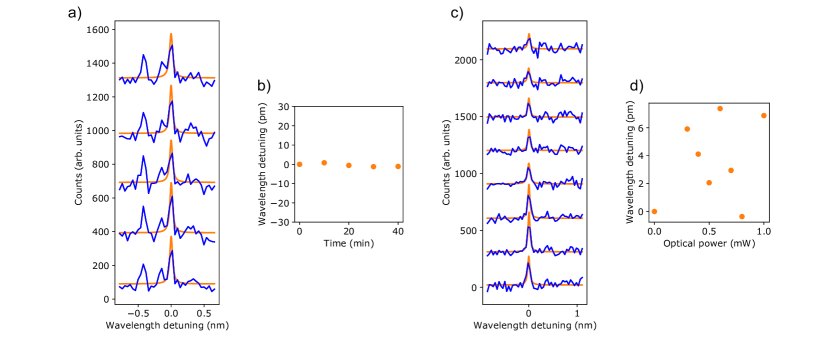
We investigated the stability of our waveguide-coupled G-centers via time-tagged PL collection. Figure S9a shows a time trace of PL emission from a single G-center during a 100 s acquisition period with a binning time of 10 ms. Figure S9b shows comparative histograms for the emitter and the waveguide background under a range of excitation powers. Our emitter histograms fit to Poisson distributions, suggesting non-blinking and stable behavior at timescales longer than 10 ms. Finally, Figure S9c shows that spectral resolution-limited PL can be observed from a single emitter in measurements separated by over a month and following multiple cryostat cooldown cycles. The spectral shift in the ZPL peak between the two measurements is likely due to recalibration of the spectrometer.
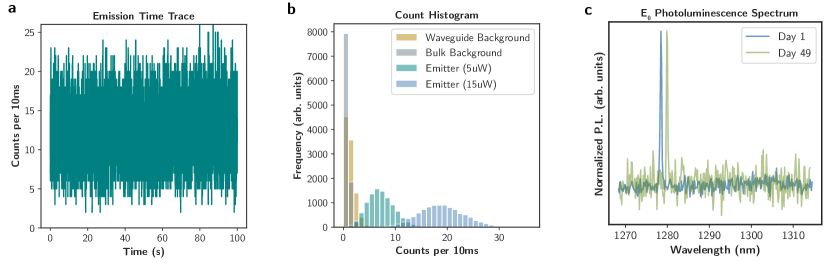
Our stability measurements are limited to a 10 ms time bin due to our limited counts arising from our low system efficiency. Higher coupling efficiencies are required to probe emitter stability at faster timescales.
.14 Optical trimming of silicon color centers
Our trimming experiments were performed in-situ in our cryogenic setup described in SI Section .5 without additional modifications. Our trimming protocol consisted of:
-
1.
Localization of emitters by PL maps using 25 µW (estimated power density of kW) of 532 nm CW laser excitation and our SNSPD detectors, followed by spectrometry (900 gr/mm grating, 40 pm resolution) under the same excitation conditions.
-
2.
Local irradiation with a 532 nm CW laser with powers in the order of 100 µW (estimated power density of kW) for 15 s.
-
3.
Characterization of the emitter by PL maps and spectrometry as in the first step.
-
4.
Repetition of steps 2-3 with increasing irradiation power.
We performed our trimming characterization protocol in 12 bright emitters (5000 to 10000 cts/s on our SNSPDs with a 1300-1550 nm bandpass filter) under PL excitation. From those, we observe trimming in 11 emitters, with spectral measurements and Lorentzian fits shown in Fig. S10 and Fig. S11b and c. We observe spectral blue shifts in 9 out of the 11 shifting emitters, while two of them red shift, including emitters in the same spatial location shifting in opposite directions. The maximum magnitude of the trimming is 300 pm (55 GHz) and depends on the emitter, with a relatively constant bandwidth limited by our spectrometer resolution. When nearing 1 mW of irradiation (estimated power density of kW), some of the emitters appear to shift back to near their original spectral position. Consecutive measurements without irradiation at any step in the process did not show spectral shift (see Fig. S11a and b for continuous monitoring of a small ensemble over 40 min). The emitter that did not show shifts showed instead diminishing brightness with increasing irradiation power, and is plotted in Fig. S11c and d. We note that we did not observe an increase in the cryostat temperature during our measurements.
For higher powers, we observe local deactivation of emitters. Figure 4d shows a PL map of a section of our waveguide containing several emitters, with a brighter ensemble in the center where the irradiation was focused. For this location, after 0.9 mW (estimated power density of kW) of local irradiation for 60 s, the small ensemble in the center is deactivated, as shown in Fig. 4e, without deactivating nearby emitters. This is evidenced by the subtracted PL map in Fig. S12, showing the location where the emitter was deactivated. The faint mark following the waveguide in Fig. S12 is a result of a slight misalignment between the first and second PL maps.

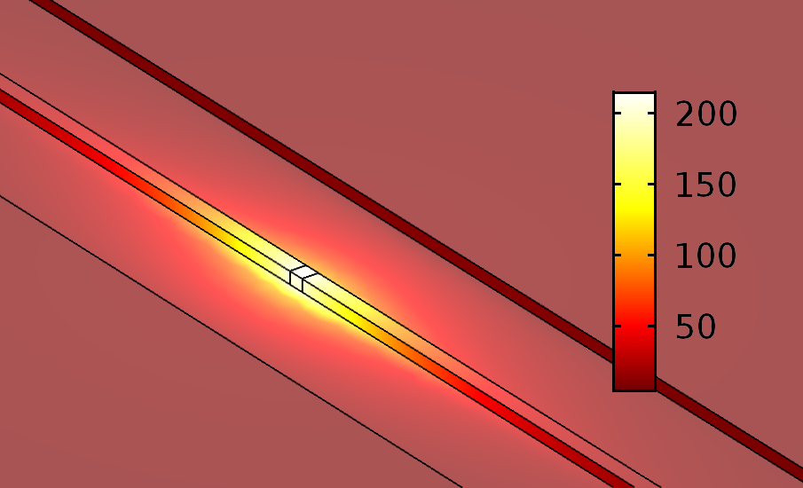
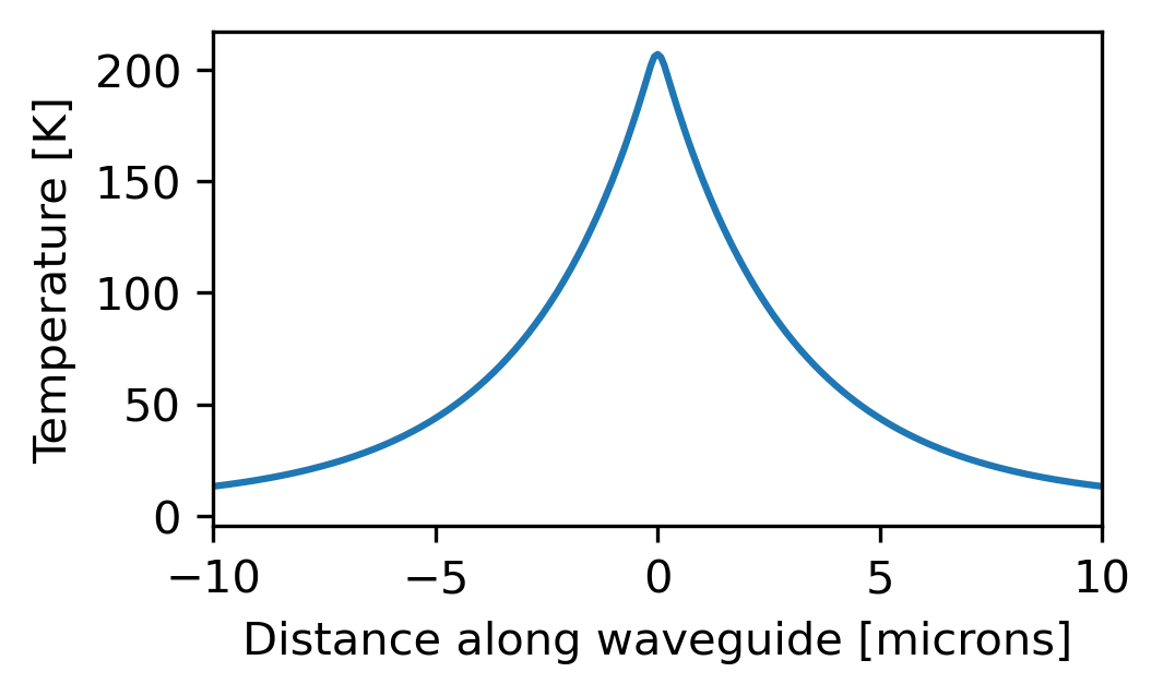
Local annealing of point defects in the waveguide could explain these observations. To explore this hypothesis, we simulate the thermal performance of our waveguide system subjected to localized heating. We assume 100 µW of heat incident upon a 300 nm300 nm square at the top of the waveguide. This corresponds to order 1 mW of 532 nm excitation: roughly a third of this power is reflected by the silicon-air interface; a tenth is assumed to be absorbed; and the remainder is absorbed in a less localized manner or reflected. The assumed absorption is estimated from silicon’s room-temperature optical attenuation coefficient of 1/µm at 532 nm Green (2008); there is evidence that the absorption coefficient at telecommunication wavelengths is roughly constant down to low temperatures Degallaix et al. (2014). We use thermal conductivity estimates at 5 K for thin silicon (10 W/m/K) and silicon dioxide (0.1 W/m/K) from Ref. Asheghi et al. (1998) and the same for the bulk silicon (100 W/m/K) substrate from Ref. Glassbrenner and Slack (1964). Note that these thermal conductivities increase with temperature for the temperature ranges considered, so our simulation with fixed conductivities overestimates the achieved temperature. Based on our simulations, we estimate an upper bound maximum temperature of 200 K at the laser spot with a full-width-half-maximum of roughly 5 µm (Fig. S13). Since these centers are stable up to room temperature and stand flash anneals at 1000∘C, the hypothesis of local annealing is thus inconsistent with our observations.
Our leading hypothesis is that the spectral shifts observed stem from DC Stark tuning arising from optically-induced charge variations, and that deactivation stems from ionization into the dark charged state of the G-center Udvarhelyi et al. (2021). Photoinduced spectral shifts have been previously reported in diamond color centers, and have been associated with trapped charges in the lattice Bassett et al. (2011). It is well known that Si/SiO2 interfaces contain a large density of hole traps Strand et al. (2018) with an experimentally-measured saturation at densities in the order of cm-2 Afanas’ev and Adamchuk (1994). We hypothesize two flavors of this effect depending on initial conditions: 1) in the presence of existing charges, optical excitation will recombine them away, resulting a more neutral state, and 2) in the absence of charges, carrier generation may result in higher densities of trapped holes. In both cases, the relative charge difference is the same, and thus in the following we estimate the effect that such charge variation can have on an artificial atom via DC Stark tuning. Given the large difference in area between our single emitters and the waveguide surface, we can assume an infinitely large charged sheet, with an associated external electric field of . is the charge density, which for SiO2 is in the order of , with the elementary charge. This estimate leads to electric fields in the order of MV/m. Assuming DC Stark tuning rates in the order of GHz/MV m, in line with other color centers such as NV in diamond Bassett et al. (2011), we estimate maximum spectral shifts in the order of GHz. We note that our estimated maximum spectral shift will be significantly affected by our device geometry and oxide interface quality (likely different between the native oxide and thermally-grown oxide at the top and bottom of our waveguide), our estimate of Stark tuning rate, or other potentially more stringent limits such as defect ionization or charge recombination effects. For high irradiation powers, one explanation is that ionization takes place, similarly to the previously reported photoionization of the NV color center in diamond Aslam et al. (2013).
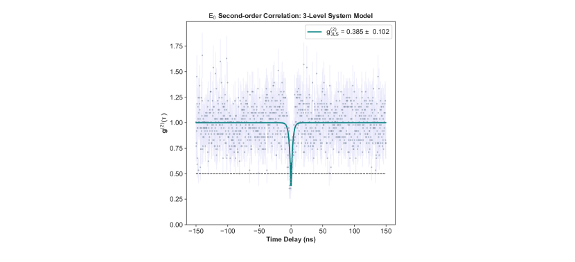
.15 Second-order correlation with a three-level atom model
The electronic level structure of the G-center defect has long been reported to consist of two singlet states and a metastable triplet state Lee et al. (1982); Udvarhelyi et al. (2021). The signature bunching effect in the second-order correlation, characteristic of a recombination process mediated by a three-level system, has been experimentally observed for G-centers in bulk SOI wafers Redjem et al. (2020); Hollenbach et al. (2020). At the excitation powers used in our measurements, we would expect to observe slight bunching near the antibunching dip at a time delay of zero. However, this measurement was limited by noise resulting from low count emitter count rates due to poor mode matching between the waveguide and collection fiber. For completeness, we include in Figure S14 the second-order correlation data presented in the main text using a 3-level system fit:
| (7) |
*