Measurements of cyclotron resonance of the interfacial states in strong spin-orbit coupled 2D electron gases proximitized with aluminum
Abstract
Two dimensional electron gasses (2DEG) in InAs quantum wells proximitized by aluminum are promising platforms for topological qubits based on Majorana zero modes. However, there are still substantial uncertainties associated with the nature of the electronic states at the interfaces of these system. It is challenging to probe the properties of these hybridized states as they are buried under a relatively thick aluminum layer. In this work we have investigated a range of InAs/InGaAs heterostructures with Al overlayers using high precision time-domain THz spectroscopy. Despite the thick metallic overlayer, we observe a prominent cyclotron resonance in magnetic field that can be associated with the response of the interfacial states. Measurements of the THz range complex Faraday rotation allow the extraction of the sign and magnitude of the effective mass, density of charge carriers, and scattering times of the 2DEG despite the close proximity of the aluminum layer. We discuss the extracted band parameters and connect their values to the known physics of these materials.
Two dimensional electron gases (2DEG) in the semiconductor quantum well heterostructures have found enormous device applications and are known to be one of the best platforms for exploring new quantum phenomenon Hopkins et al. (1991); Ikebe et al. (2010); Spivak et al. (2010); Shabani et al. (2016). This is possible due to the ease of tuning their properties like charge carrier density, mass and mobility. These properties of 2DEGs have been mostly studied using dc transport based techniques like magnetoresistance. Non-contact probes like IR and Terahertz spectroscopy have been used less often to investigate their properties. Motivated by theoretical predictions of topological superconductivity in semiconductor–superconductor heterostructures with possible applications in quantum-information processing Lutchyn, Sau, and Das Sarma (2010); Oreg, Refael, and von Oppen (2010), there has been a huge surge in interest in semiconductor-superconducting hybrids systems in the past decade Chang et al. (2015); Kjaergaard et al. (2016); Nichele et al. (2017). Some of the more popular hybrids utilize clean elemental metals which are highly conducting as the superconducting component. Examples of this are Al-InAs, Sn-InSb Pendharkar et al. (2021), Ta-InAs Carrad et al. (2020) and Pb-InAs Kanne et al. (2021); Drachmann et al. (2021). 2DEG quantum well heterostructures based on semiconductors with large Rashba spin-orbit coefficient like InAs and InSb have been found to be most successful for such applications Shabani et al. (2016); Lutchyn et al. (2018).
Although the progress in developing these hybrid heterostructures has been impressive, there are still substantial uncertainties associated with the nature of their interfacial states. Once the highly conducting overlayer is deposited on the semiconducting heterostructure, their coupling can modify the properties of the interface. Contact based probes have the problem of electrical shorting from the highly conducting layer, making it extremely challenging to study the properties of the 2DEG buried below the metallic overlayer Schuwalow et al. (2021). In many cases, properties of the 2DEG can only be studied by removing the metallic overlayer. Below we detail our development of a measurement scheme to explore the properties of the 2DEG with a highly conducting overlayer using THz-TD magneto-spectroscopy to overcome this challenge. Such experiments can isolate the cyclotron resonance (CR) response of the 2DEG, as well has having a number of advantages over traditional transport experiments.
In the present work, we use high precision time-domain magnetoterahertz spectroscopy with polarization modulation in transmission configuration to investigate the CR response in Faraday rotations from the 2DEG in a planar InAs quantum well - aluminum heterostructures. These experiments, as they measure the frequency and field dependence dependence of a complex response function provide a great deal of information. In other contexts they have been able to provide the mass, mobility, and density of multiple conducting channels simultaneously Cheng et al. (2019a). In the present case, we observe a prominent THz frequency CR response from the 2DEG in magnetic fields up to 3 T. These experiments are sensitive almost exclusively to the 2DEG because of the much smaller mass of the semiconductor layer as compared to that of the elemental metal. By measuring and modeling the THz range complex Faraday rotation we extract the parameters like the sign and magnitude of the effective mass, density of charge, and scattering times. Our measurement scheme demonstrates for the first time that it is possible to extract the parameters of a 2DEG that is buried under much more conductive layer by measuring the CR response.
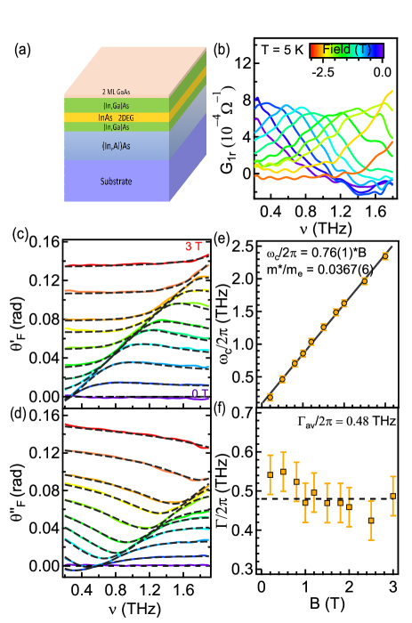
The thin film quantum well heterostructures used in this work were grown by molecular beam epitaxy on 0.5 mm thick undoped InP substrate wafer in (100) crystal orientation whose lateral size was . The main layers of importance in the heterostructure can be seen in the schematic cross section in Fig. 1(a). The 7 nm wide InAs quantum well (yellow layer), is sandwiched by top 10 nm In0.80Ga0.20As barrier and bottom 4 nm In0.81Ga0.19As layer (green) and capped with a 2 ML GaAs layer. 7 nm of Al overlayer was deposited on top; approximately 2 nm oxidizes to AlO and leaves an effectively 5 nm Al layer on top of the barrier [see Fig. 2(a)]. TDTS experiments were performed in a home-built time-domain terahertz spectrometer with a 7 T magnet in closed cycle cryostat. On one sample Al was etched off by standard wet etch methods. Measurements were performed in Faraday geometry meaning both the magnetic field and light propagation direction were same. Both the real and imaginary part of the complex optical conductance and the Faraday rotation were extracted from the measured complex transmission at 5 K as shown in Refs. tra, ; Cheng et al., 2019b. Using the polarization modulation technique Morris et al. (2012), we obtain the complex transmission in right- and left-circularly polarized bases ( and ) as it is the transmission eigenbasis for a time-reversal symmetry breaking square system. We use linearly polarized light and extract out the diagonal and off diagonal components of the Jones transmission matrix and then transform to the right- and left-circularly polarized bases via Armitage (2014).

Fig. 1(b) shows the field dependent real part of the righthand circularly polarized sheet conductance at 5 K obtained from the complex transmission tra ; Cheng et al. (2019b). The spectra at zero field show a tail of narrow Drude-like term. At finite field a dip is observed to shift with increasing magnetic field, which is consistent with a CR that depends on field in the usual way . The width of the dip given by its full-width at half maximum (FWHM) is a measure of the scattering rate , while its area is a measure of the charge density . To get a more accurate measure of these quantities we extract and analyze the complex Faraday rotation.
We obtain the complex Faraday rotation from the right- and left-hand complex transmission using the expression . The gives the rotation of the major axis of light and the relates to the ellipticity Morris et al. (2012). Field dependent real () and imaginary () parts of the up to 3 T are shown in Fig. 1(c)-(d). Note that we have uncertainties with field (i.e. ) in order to eliminate a number of systematic errors. An inflection point in and the dip in are observed to shift higher in frequency with increasing magnetic field, which is in accordance with the known behavior of CR with .
In order to extract the exact CR frequencies and other parameters at different fields, we fit the complex to the Drude model. The expression for a single Drude oscillator’s magneto-conductance is
| (1) |
Here, the sign signifies the use of right- or left-hand circularly polarized light, respectively. is the plasma frequency, d is the film thickness, is the CR frequency, is the scattering rate, and is the background dielectric constant that originates from lattice polarizibility and excitations at frequencies well above the measured spectral range. The spectral weight relates to the carrier density () and the effective transport mass () as . The complex Faraday rotation angle can be expressed in terms of right- and left-circularly polarized optical conductance as,
| (2) |
As shown in Fig. 1(c)-(d), fits to this model while accounting for the field dependence of the Drude term are in good agreement with both the real and imaginary parts of the complex . The parameters for the spectral weight and are constrained by doing a global fit to the entire field dependent , leaving the cyclotron frequency and the scattering rate as the only free parameters at each field which allows for their extraction as a function of the magnetic field [see Fig. 1(e)-(f)]. As expected, the cyclotron resonance frequency has linear dependence on the field. The relation between carrier mass and resonance frequency (given by Wu et al. (2015), a fit to the is shown in Fig. 1(e)) gives the cyclotron mass of the electrons in this 2DEG without an Al overlayer to be , where is the free electron mass. Then using the relation, and spectral weight obtained from fitting the Faraday rotation we extract the total sheet carrier density cm-2. The extracted scattering rate of the carriers in field as shown in Fig. 1(f), does not show strong field dependence and has an average of THz. We determine the mobility of the 2DEG carriers to be cmVs.
The above analysis gives us important insight into the properties of the 2DEG in a planar heterostructure. Some of this information can be inferred from conventional transport experiments, but once a highly conductive overlayer like Al is deposited on top of such a heterostructure (e.g. superconductor-semiconductor devices), it becomes impossible to access the properties of 2DEG using such techniques. The TDTS CR resonance experiments still provide important information as the effective mass of the aluminum layer is of order the free electron mass, which (when considering the large scattering in the Al layer) is large enough that it does not exhibit a prominent CR. Therefore the conductance of the Al layer is almost field independent. As it is a resonance effect, the CR of the 2DEG is still detectable even with transmission greatly decreased because of the Al layer.
We now use the same method of magnetoterahertz spectroscopy to measure the 2DEG on a similar InAs quantum-well heterostructure, but one with an Al overlayer. Through precise measurements of the complex we can determine the properties of the 2DEG below the metallic overlayer. The schematics of the measured heterostructure with 5 nm Al overlayer is shown in Fig. 2(a). In Fig. 2(b) we show the real part of the zero field sheet conductance of both the entire heterostructure as well as a similarly prepared structure that has no 2DEG (e.g. that is just Al). One can see that the overall scale of the conductance is much larger than that of the 2DEG (Fig. 1(b)). The conductive layers of the heterostructure (2DEG and Al overlayer) can be treated as parallel conductance channels, so the total conductance will be sum of their individual conductances; thus allowing for larger conductance of the heterostructure in comparison to just Al. for heterostructure with Al is two orders of magnitude larger than the ones without Al [see Fig. 1(b)], showing the large contribution of Al () in the effective conductance of the entire heterostructure. The field dependence of the heterostructure conductance up to 3 T is shown in the inset of Fig. 2(b). A broad feature can be observed to shift with field but the large background of makes finding the difficult. In order to better understand the 2DEG properties we look at the in-field Faraday rotation, as response is largely set by the properties of the 2DEG.
The antisymmetrized complex obtained from the complex transmission is shown in Fig. 3(c)-(d). The maximum amplitude of the for the sample with Al is times smaller than the sample without Al, implying the suppression of angle in heterostructures with Al. From Eq.(2), the Faraday rotation depends on the total conductance of the sample, which is the sum of conductances of the heterostructure and Al. The reduction in the rotation angle is due to the Al overlayer as the Al conductance’s field dependence is small. The complex Faraday rotation angle with the Al overlayer is
| (3) |
Here, and are the conductances for the heterostrusture and the Al overlayer, respectively. Fits to this model of complex while constraining the spectral weight and by doing a global fit to all the measured fields are shown in Fig. 2(c)-(d). The fits use only a single Drude term and are in reasonably good agreement with the data. The frequency independent contribution from the Al overlayer was accounted for by doing a separate measurement of a 5 nm Al thin film as shown in Fig. 2(b). In Fig. 2(e), the linear fit of verses B gives an effective CR mass of , which is slightly higher than for the sample without Al overlayer. It has larger spectral weight ( THzm) than the sample without Al, giving higher charge density of cm-2. The scattering rate of this sample as shown in Fig. 2(f) is approximately constant with field. The average scattering rate of THz gives a mobility of cms.
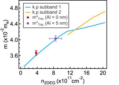
In order to gain further insight into the the 2DEG band structure, we model the quantum well and barrier layers with an 8-band model Foreman (1997); Winkler (2003); Vurgaftman, Meyer, and Ram-Mohan (2001). The quantum model covers the top 25 nm of the semiconductor stack and is self-consistently coupled to a Poisson solver, which solves for the electrostatic potential between a fixed band offset at the surface and a Neumann boundary 1.5 m deep in the substrate. By varying the band offset at the surface, we find that the measured densities are reproduced when the Fermi level is pinned close to (80 meV above) the conduction band edge () at the semiconductor/vacuum (semiconductor/aluminum) interface, respectively. Both samples (with and without Al) have a single subband, whose density is predominantly located in the InAs quantum well. The subband’s cyclotron mass increases monotonically with density [See Fig. 3], as expected for a nonparabolic 2D band where the cyclotron mass grows with Fermi energy. The fact that the measured density and mass values lie directly on the predicted curve is a nontrivial consistency check because the model has no free parameters beyond the band offset that was swept to produce the curve.
Our measurements give the most accurate determination of parameters of 2DEGs hybridized with aluminum overlayers. Importantly, our experiments can measure parameters relevant to the 2DEG despite the large conductive background given by the aluminum. In Table I, we give the fitted parameters for samples without and with the Al overlayer (as well as aluminum to compare). One can see that the samples with an Al overlayer have a substantially increased density and moderately increased mass. This can be compared to calculations that match well the experiment to within experimental uncertainties. It is important to note that the the agreement is good for the aluminum overlayer samples despite the fact that theoretical calculations do not explicitly include hybridization with aluminum states. That there is appreciable coupling nevertheless can be seen from that fact that when this structure is cooled down below Tc there will be a large induced gap eV in the semiconductor Nichele et al. (2017). One might infer from this that the hybridization is small at least in comparison to the rate set by the measurement frequency. It is also interesting to note that the mobility of these 2DEGs do not appreciably change with etching, which presumably introduces disorder. This is particularly remarkable because the etched samples have lower density and the effects of disorder on mobility are expected to be larger at low density. The lack of change may be due to the fact that for the higher density aluminum covered samples, the electron lives in a double well potential with an appreciable part of its wavefunction on the surface. It is likely that the effect of the wavefunction shifting away from the surface in the etched sample compensates for the larger disorder and its effects at lower densities.
| System | n (cm-2) | cmV s | (meV) | |
|---|---|---|---|---|
| InAs | 0.0367(6) | |||
| Al-InAs | 0.0403(7) | |||
| Al | 1.4 | - | - |
Acknowledgements.
The work at JHU and Purdue was supported by Microsoft Quantum. Our calculations made use of the semicon Sko and Kwant Groth et al. (2014) packages.References
- Hopkins et al. (1991) P. F. Hopkins, A. J. Rimberg, R. M. Westervelt, G. Tuttle, and H. Kroemer, “Quantum Hall effect in InAs/AlSb quantum wells,” Applied Physics Letters 58, 1428–1430 (1991), https://doi.org/10.1063/1.105188 .
- Ikebe et al. (2010) Y. Ikebe, T. Morimoto, R. Masutomi, T. Okamoto, H. Aoki, and R. Shimano, “Optical Hall Effect in the Integer Quantum Hall Regime,” Phys. Rev. Lett. 104, 256802 (2010).
- Spivak et al. (2010) B. Spivak, S. V. Kravchenko, S. A. Kivelson, and X. P. A. Gao, “Colloquium: Transport in strongly correlated two dimensional electron fluids,” Rev. Mod. Phys. 82, 1743–1766 (2010).
- Shabani et al. (2016) J. Shabani, M. Kjærgaard, H. J. Suominen, Y. Kim, F. Nichele, K. Pakrouski, T. Stankevic, R. M. Lutchyn, P. Krogstrup, R. Feidenhans, et al., “Two-dimensional epitaxial superconductor-semiconductor heterostructures: A platform for topological superconducting networks,” Physical Review B 93, 155402 (2016).
- Lutchyn, Sau, and Das Sarma (2010) R. M. Lutchyn, J. D. Sau, and S. Das Sarma, “Majorana fermions and a topological phase transition in semiconductor-superconductor heterostructures,” Phys. Rev. Lett. 105, 077001 (2010).
- Oreg, Refael, and von Oppen (2010) Y. Oreg, G. Refael, and F. von Oppen, “Helical Liquids and Majorana Bound States in Quantum Wires,” Phys. Rev. Lett. 105, 177002 (2010).
- Chang et al. (2015) W. Chang, S. M. Albrecht, T. S. Jespersen, F. Kuemmeth, P. Krogstrup, J. Nygård, and C. M. Marcus, “Hard gap in epitaxial semiconductor-superconductor nanowires,” Nature Nanotechnology 10, 232–236 (2015).
- Kjaergaard et al. (2016) M. Kjaergaard, F. Nichele, H. J. Suominen, M. P. Nowak, M. Wimmer, A. R. Akhmerov, J. A. Folk, K. Flensberg, J. Shabani, C. J. Palmstrøm, and C. M. Marcus, “Quantized conductance doubling and hard gap in a two-dimensional semiconductor-superconductor heterostructure,” Nature Communications 7, 12841 (2016).
- Nichele et al. (2017) F. Nichele, A. C. C. Drachmann, A. M. Whiticar, E. C. T. O’Farrell, H. J. Suominen, A. Fornieri, T. Wang, G. C. Gardner, C. Thomas, A. T. Hatke, P. Krogstrup, M. J. Manfra, K. Flensberg, and C. M. Marcus, “Scaling of Majorana Zero-Bias Conductance Peaks,” Phys. Rev. Lett. 119, 136803 (2017).
- Pendharkar et al. (2021) M. Pendharkar, B. Zhang, H. Wu, A. Zarassi, P. Zhang, C. P. Dempsey, J. S. Lee, S. D. Harrington, G. Badawy, S. Gazibegovic, R. L. M. O. het Veld, M. Rossi, J. Jung, A.-H. Chen, M. A. Verheijen, M. Hocevar, E. P. A. M. Bakkers, C. J. Palmstrøm, and S. M. Frolov, “Parity-preserving and magnetic field-resilient superconductivity in insb nanowires with sn shells,” Science 372, 508–511 (2021), https://www.science.org/doi/pdf/10.1126/science.aba5211 .
- Carrad et al. (2020) D. J. Carrad, M. Bjergfelt, T. Kanne, M. Aagesen, F. Krizek, E. M. Fiordaliso, E. Johnson, J. Nygård, and T. S. Jespersen, “Shadow epitaxy for in situ growth of generic semiconductor/superconductor hybrids,” Advanced Materials 32, 1908411 (2020), https://onlinelibrary.wiley.com/doi/pdf/10.1002/adma.201908411 .
- Kanne et al. (2021) T. Kanne, M. Marnauza, D. Olsteins, D. J. Carrad, J. E. Sestoft, J. de Bruijckere, L. Zeng, E. Johnson, E. Olsson, K. Grove-Rasmussen, and J. Nygård, “Epitaxial pb on inas nanowires for quantum devices,” Nature Nanotechnology 16, 776–781 (2021).
- Drachmann et al. (2021) A. C. C. Drachmann, R. E. Diaz, C. Thomas, H. J. Suominen, A. M. Whiticar, A. Fornieri, S. Gronin, T. Wang, G. C. Gardner, A. R. Hamilton, F. Nichele, M. J. Manfra, and C. M. Marcus, “Anodic oxidation of epitaxial superconductor-semiconductor hybrids,” Phys. Rev. Materials 5, 013805 (2021).
- Lutchyn et al. (2018) R. M. Lutchyn, E. P. Bakkers, L. P. Kouwenhoven, P. Krogstrup, C. M. Marcus, and Y. Oreg, “Majorana zero modes in superconductor–semiconductor heterostructures,” Nature Reviews Materials 3, 52–68 (2018).
- Schuwalow et al. (2021) S. Schuwalow, N. B. Schröter, J. Gukelberger, C. Thomas, V. Strocov, J. Gamble, A. Chikina, M. Caputo, J. Krieger, G. C. Gardner, et al., “Band structure extraction at hybrid narrow-gap semiconductor–metal interfaces,” Advanced Science 8, 2003087 (2021).
- Cheng et al. (2019a) B. Cheng, P. Taylor, P. Folkes, C. Rong, and N. Armitage, “Magnetoterahertz response and faraday rotation from massive dirac fermions in the topological crystalline insulator pb 0.5 sn 0.5 te,” Physical review letters 122, 097401 (2019a).
- (17) In the thin film limit, the conductance can be extracted using the equation, . Here, is the complex conductance in the eigenbasis of the transmission, is the refractive index of the substrate, is the vacuum impedance, and is the thickness difference between the sample and reference substrates.
- Cheng et al. (2019b) B. Cheng, Y. Wang, D. Barbalas, T. Higo, S. Nakatsuji, and N. P. Armitage, “Terahertz conductivity of the magnetic Weyl semimetal Mn3Sn films,” Applied Physics Letters 115, 012405 (2019b), https://doi.org/10.1063/1.5093414 .
- Morris et al. (2012) C. M. Morris, R. V. Aguilar, A. V. Stier, and N. P. Armitage, “Polarization modulation time-domain terahertz polarimetry,” Opt. Express 20, 12303–12317 (2012).
- Armitage (2014) N. Armitage, “Constraints on Jones transmission matrices from time-reversal invariance and discrete spatial symmetries,” Physical Review B 90, 035135 (2014).
- Wu et al. (2015) L. Wu, W.-K. Tse, M. Brahlek, C. M. Morris, R. V. Aguilar, N. Koirala, S. Oh, and N. P. Armitage, “High-resolution faraday rotation and electron-phonon coupling in surface states of the bulk-insulating topological insulator ,” Phys. Rev. Lett. 115, 217602 (2015).
- Foreman (1997) B. A. Foreman, “Elimination of spurious solutions from eight-band theory,” Phys. Rev. B 56, R12748–R12751 (1997).
- Winkler (2003) R. Winkler, Spin-orbit coupling effects in two-dimensional electron and Hole Systems, Springer Tracts in Modern Physics, Vol. 191 (Springer, 2003).
- Vurgaftman, Meyer, and Ram-Mohan (2001) I. Vurgaftman, J. R. Meyer, and L. R. Ram-Mohan, “Band parameters for iii–v compound semiconductors and their alloys,” Journal of Applied Physics 89, 5815–5875 (2001), https://doi.org/10.1063/1.1368156 .
- Ashcroft and Mermin (1976) N. W. Ashcroft and N. D. Mermin, Solid State Physics (Holt-Saunders, 1976).
- Lin et al. (2015) S.-W. Lin, Y.-H. Wu, L. Chang, C.-T. Liang, and S.-D. Lin, “Pure electron-electron dephasing in percolative aluminum ultrathin film grown by molecular beam epitaxy,” Nanoscale Research Letters 10, 71 (2015).
- (27) R. Skolasinski et al., https://gitlab.kwant-project.org/semicon/semicon.
- Groth et al. (2014) C. W. Groth, M. Wimmer, A. R. Akhmerov, and X. Waintal, “Kwant: a software package for quantum transport,” New Journal of Physics 16, 063065 (2014).