Non-contact Andreev reflection as a direct probe of superconductivity on the atomic scale
Abstract
Direct detection of superconductivity has long been a key strength of point-contact Andreev reflection. However, its applicability to atomic-scale imaging is limited by the mechanical contact of the Andreev probe. To this end, we present a new method to probe Andreev reflection in a tunnel junction, leveraging tunneling spectroscopy and junction tunability to achieve quantitative detection of Andreev scattering. This method enables unambiguous assignment of superconducting origins of current-carrying excitations as well as detection of higher order Andreev processes in atomic-scale junctions. We furthermore revealed distinct sensitivity of Andreev reflection to natural defects, such as step edges, even in classical superconductors. The methodology opens a new path to nano- and atomic-scale imaging of superconducting properties, including disordered superconductors and proximity to phase transitions.
Notice: This manuscript has been authored by UT-Battelle, LLC, under Contract No. DE-AC0500OR22725 with the U.S. Department of Energy. The United States Government retains and the publisher, by accepting the article for publication, acknowledges that the United States Government retains a non-exclusive, paid-up, irrevocable, world-wide license to publish or reproduce the published form of this manuscript, or allow others to do so, for the United States Government purposes. The Department of Energy will provide public access to these results of federally sponsored research in accordance with the DOE Public Access Plan (http://energy.gov/downloads/doe-public-access-plan).
Andreev reflection (AR) occurs when electron traverses normal metal to superconductor interface, wherein a hole is retroreflected back into the metal and a Cooper pair is injected into the superconductor Andreev (1964); Tinkham (2004). By utilizing sharp metallic wire to make mesoscale contact with superconductors, point-contact AR (PCAR) has been developed as a very successful technique to probe the fundamental properties of superconductors Naidyuk and Yanson (2005); Daghero et al. (2013). PCAR measurements are frequently interpreted with the Blonder-Tinkham-Klapwijk (BTK) formalism, which allows accounting both for BCS s-wave superconductivityBlonder et al. (1982), unconventional and multiband superconductivityKashiwaya et al. (1996); Brinkman et al. (2002). While conventional Andreev reflection is currently well understood, atomic-scale tunneling techniques exploiting this phenomena for sensing the nature of substrate carriers have remained relatively unexplored.
Scaling down Andreev measurements to nano- and even atomic-scales would provide a definitive methodology to directly probe microscopic properties of superconductivity, such as effects of disorder Dubouchet et al. (2018), competing order parameters Park et al. (2008), interfaces Oh et al. (2021) and topological defects Tanaka et al. (2009); Zhu et al. (2020), extending and complementing nanoscale measurements of quasiparticle density of states in scanning tunneling microscopy (STM) Pan et al. (1998); Hoffman et al. (2002) and break junctions van der Post et al. (1994); Scheer et al. (1998). However, bringing point contact measurements such as PCAR to atomic-scale measurements faces distinct challenges. On the one hand, atomic contacts are mostly random, invasive (causing local surface damage) and poorly controlled Tartaglini et al. (2013), likely even more so for complex surfaces of unconventional superconductors such as cuprates Wei et al. (1998) and iron-based superconductors Daghero et al. (2011). Meanwhile, the theoretical models would have to be extended to account for the atomic-scale contact geometry, unconventional order parameters and multiband gap structuresDaghero et al. (2013).
In this letter, we develop a non-contact Andreev reflection (NCAR) technique based on scanning tunneling microscopy/spectroscopy (STM/S). The technique contributes tunability of junction geometry and tunneling spectroscopy to the measurement of Andreev reflection. However, it does so at the expense of direct measurement of contact conductance, which is the fundamental observable in PCAR Naidyuk and Yanson (2005). To address this apparent challenge we exploit the relative probability of tunneling between normal and Andreev process as a robust observable sensitive to local Andreev reflection Ko et al. (2021). The relative probability is quantified by measuring normalized decay rate of tunneling current with low-temperature STM, combined with detailed tight-binding modeling. The method emerges as an effective and direct probe of superconductivity up to the superconducting transition temperature (). Moreover, our methodology directly reveals the order of the tunneling process responsible of the current, and the inhomogeneity of Andreev reflection due to single atomic steps even in classical superconductors. This combination of non-contact and near-contact Andreev reflection (NeCAR) enriches the spectrum of properties accessible with nano and atomic-scale resolution, enabling new insight into local properties of both classical and exotic superconductors.
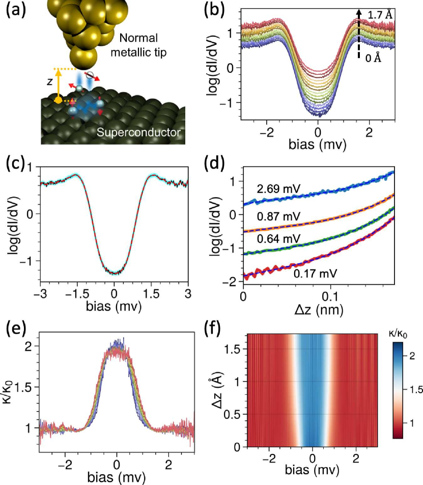
To reveal the properties of NCAR, we carried out detailed spectroscopy of normal metal - superconductor tunnel junction in well-understood Pb(110) as a model system [Fig. 1(a)]. The atomically clean surface of Pb(110) was prepared by repeating sputtering-annealing cycles Ruby et al. (2015). The experiments were performed in SPECS JT-STM operated at ultrahigh vacuum condition ( mbar) and base operating temperature of 1.2 K. The quality of STM tip was checked on either Au(111) or Cu(111) single crystals, and further conditioned by pulsing and soft crashes until the tip displayed proper metallic behavior. The - curves were acquired by sweeping direct current bias without any additional electrical signals. The differential conductance were obtained by numerical differentiation of the - curves. To minimize the noise in numerical differentiation, the analysis of the decay rate was carried out by fitting numerically obtained with Gaussian process regression [Fig. 1(b)]Pedregosa et al. (2011), which provides effective interpolation as well as a robust noise-level estimation. We utilized a simple kernel that is a sum of squared-exponential and white noise. We found the performance of this algorithm to be robust toward the choice of initial values and kernel parameters.
To detect Andreev reflection, spectra were measured as a function of the distance between the tip and the sample [Fig. 1(c)]. increases nearly exponentially both inside and outside of the superconducting gap. Exact height dependence was extracted from - curves at each bias [Fig. 1(d)], which can be well fit with an exponential function in tunneling regime (i.e. at tunneling conductance ). One prominent feature is that although the amplitude changes, its slope in - curve, i.e. decay rate , is almost constant outside of the superconducting gap. However, for the bias inside the gap, the slope significantly increases, which reflects a change of the dominant tunneling mechanism (conceptually similar to our previous approach to differentiate between Andreev and Josephson currents Ko et al. (2021)). Because of the normal-superconducting junction in the present case, the lowest order contribution to change in the tunneling decay rate is the onset of Andreev reflection.
The change in was further quantified by calculating its dependence on bias from the fitted by Gaussian process regression, and subsequently normalizing by the decay rate of normal tunneling measured well outside the superconducting gap. This procedure should account for the variation of the decay rate in the normal tunneling regime, such as geometrical and chemical structure of the tunnel junction. The resulting normalized decay rate should now be primarily sensitive to the superconducting state. As seen in Fig. 1(f), maintains approximately constant value of 1 outside the gap, and it increases to a value of approximately 2 inside the gap. These are exactly the values expected for transition from single charge tunneling to Andreev reflection Cuevas et al. (1996); Cuevas and Belzig (2003); Johansson et al. (2003). Moreover, is only weakly dependent on the specific value of tunneling conductance (set by tip-surface height) in the tunneling regime. As the tip brought closer to the surface, only the bias range where becomes wider, which is displayed more clearly in the colormap plot of as a function of bias and [Fig. 1(e)]. The observation indicates that the Andreev reflection becomes more prominent at the gap edge as the tunneling barrier gets narrower.
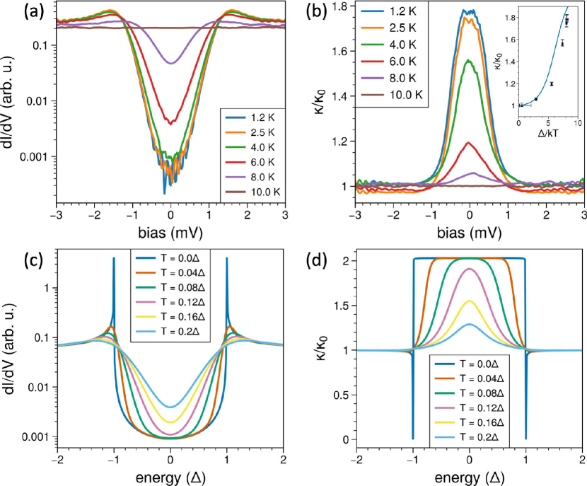
Several factors can induce the deviation from ideal value of of Andreev reflection, most prominently instrumental and thermal broadening. Figure 2(a) and 2(b) shows the spectra and normalized decay rate, respectively, as temperature increased from 1.2 K to 10 K. The superconducting gap in displays both thermal broadening and gap closing as temperature is increased, until there is no gap as at 10 K. Meanwhile, shows a plateau near the value of 2 at zero bias for lowest temperature of 1.2 K, but then the maximum value steadily decreases and the bias range where narrows as temperature increases, ultimately reaches 1 for all biases at when at 10 K. Closely correlated changes in and the magnitude of the superconducting gap independently confirm the detection of Andreev reflection. The reverse relationship can also be stated - observation of increasing to a maximum of 2 inside the gap identifies the origin of the gap as being most likely due to superconductivity. This is particularly important for a broad array of new emerging materials Liu et al. (2021); Zhao et al. (2021) as well as confined geometries of nanowires and nanoparticles Bezryadin et al. (2000), where superconducting states are sought but competing ordered states, e.g. charge density wave, can manifest instead.
Theoretical modeling of NCAR was carried out with tight-binding simulations. From the theoretical point of view, we model our tunnel junction with the full Hamiltonian , where we consider an effective one-dimensional transport geometry between the tip and the sample. We take a normal state tip a superconducting substrate and a height-dependent tunneling coupling between the tip and the sample . parametrizes the distance-dependent tunneling amplitude between tip and sample, that takes the form with the decay constant 111We will take , leading to a perfectly transparent regime for at . In the tunneling regime, leading-order perturbation theory yields a conductance proportional to for normal metal transport, and for Andreev tunneling. The normalized decay rate is given by where and are the decay rates of the absence and presence of a superconducting gap, defined as evaluated at a bias and distance to the sample . We compute the and factor using the non-perturbative -matrix formalism implemented with finite temperature non-equilibrium Nambu Green’s functions Datta (1995); Blonder et al. (1982); Sancho et al. (1985); Fisher and Lee (1981); Brand et al. (2018); pyq . Within this formalism, the differential conductance is computed exactly both in the tunneling and contact regimes at finite temperature.
Our theoretical calculations shown in Fig. 2(c) and 2(d) show that the temperature dependence accounts for both the smearing of the dI/dV spectra and the thermal renormalization of the decay rate. At zero temperature and inside the superconducting gap, the current is carried by Andreev reflection, involving two-tunneling events with . In the normal state, the current is carried by single charge tunneling with . At finite temperatures and inside the superconducting gap, both tunneling processes compete, giving rise to between 1 and 2. Inside the gap, and as the temperature is lowered, Andreev reflection becomes increasingly dominating, reaching the value of 2 for low enough temperatures. The transition can be parametrized by plotting maximum as a function of the ratio between the superconducting gap and temperature [Inset of Fig. 2(b)]. The experimental points in the plot displays a very good match to the theoretical curve, which indicates among other things that the tight-binding model properly reflects the tunneling process of NCAR.
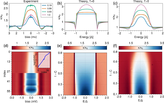
So far, our measurements and calculations point to a maximum value of of 2 in the tunneling limitCuevas et al. (1996); Cuevas and Belzig (2003); Johansson et al. (2003). Interestingly, at near-contact tunneling conductance we have also measured values in excess of 2 [Fig. 3(a)], whose origin reflects a much richer physical scenario in comparison with the tunneling regime. To address this question systematically, we have applied the normalized decay rate methodology to the near-contact regime, where tunneling conductance begins to approach quantum conductance , as shown in Fig. 3. In contrast to the tunneling window in Fig. 1(f), the spectra undergo a dramatic change as tip reaches near contact [Fig. 3(a,d)]. The center of plateau far exceeds the maximum value of for the tunneling regime, reaching up to . Meanwhile, at the edges of the superconducting gap, the reduces below 1, implying that the transmission is becoming more favorable than in the normal regime. Then, as the tip is brought even closer, the normalized decay rate in the middle of the superconducting gap begins to reduce. All these properties signify a distinct regime of Andreev reflection, that is intermediate between NCAR and PCAR (which we refer to as NeCAR below), corresponding to simultaneous enhancement and suppression of Andreev reflection and its strong energy dependence.
We now elaborate on the physical interpretation of the normalized decay rate in near contact regime. From a perturbation theory point of view, the decay rate directly signals the order of the term in perturbation theory dominating the current. In the tunneling limit of the normal state the leading contribution comes from second order in the coupling constant, whereas in the tunneling limit of Andreev reflection it comes from fourth order in the coupling constant, leading to a normalized ratio . For near contact regime, besides the lowest order terms in perturbation theory higher order terms lead to competing contributions in the current Mélin and Feinberg (2004); Falci et al. (2001); Bignon et al. (2004), such as sixth order in the coupling, leading to a normalized ratio . As a result, the normalized decay rate is a direct probe of the order of the process responsible for the tunneling current as well as the nature of the current carriers in the substrate.
Furthermore, the enhancement of tunneling at the superconducting gap edge, which is marked by reduced , is the signature of resonant tunneling to the superconducting gap edgeDatta (1995). The existence of a resonant process is directly accounted by the quantum transport formalism, and our experiment demonstrates its first unequivocal detection by NeCAR. Although in principle resonant tunneling should also be observed in the tunneling regime [Fig. 3(b,e)], the resonance is extremely sharp and disappears when there is finite thermal broadening [Fig. 3(c,f)]. However, around near contact, resonant tunneling starts to happen for broader bias range and it becomes detectable with spectroscopy. Tight-binding simulation at finite temperature reproduced all experimental features we observed at NeCAR [Fig. 3(c,f)], showing that a phenomenology is fully captured by our theoretical model.
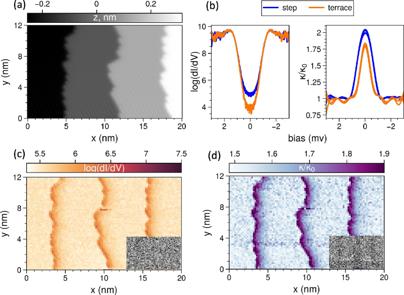
Clearly, the compatibility of NCAR and NeCAR spectroscopies with STM junction enables microscopic measurements in both regimes down to atomic resolution. Intriguingly, NCAR revealed a new signatures of single atomic steps even on well-established Pb superconductor. Figure 4 shows the results of spectroscopy grid over an area of Pb(110) with single atomic steps shown in Fig. 4(a). The steps show distinct contrast in both and . Tunneling conductance is mainly seen to be enhanced in the narrow region around the gap center [Fig. 4(b,c)], although the estimation of the size of the superconducting gap from the coherence peak position results in the same value for terrace and step within the measurement error [Fig. 4(b)] and also as confirmed by Dynes fit Dynes et al. (1978). Meanwhile, spectroscopy reveals that this difference is related not to single-charge density of states but to Andreev reflection, which is noticeably enhanced at the single atomic steps compared to surrounding terraces [Fig. 3(b,d)]. The result indicates that single-charge DOS is nearly identical between the steps and terraces while Andreev reflection is significantly enhanced at the steps. In fact, from the perspective of Andreev reflection, the steps behave as though the superconductivity is locally enhanced, by comparison with the temperature effect in Fig. 2(b). The origin of this enhancement remains to be understood. We hypothesize that it may be related to the reduced dimensionality of the step edge, and the concomitant effect on the local electronic structure sensitively probed through Andreev reflection.
To summarize, we have put forward NCAR as a powerful method for characterizing superconducting properties on nanoscale. Our methodology detects Andreev reflection by via a connection between the decay rate of the tunneling current and the order of the term in perturbation theory describing the current mechanism. We showed that NCAR can unequivocally distinguish a superconducting gap from other types of single-particle gaps. Furthermore, at near contact our methodology detects next to leading order Andreev reflection processes, which is distinct from both contact and tunneling regimes. Even in conventional s-wave Pb superconductor, mapping NCAR signal exhibited enhancement of Andreev reflection at single atomic steps, providing a powerful method to image current carrying excitations at the atomic scale. In the future, this technique can be readily extended to the emerging families of unconventional and topological superconductors Liu et al. (2021); Zhao et al. (2021); Dubouchet et al. (2018); Oh et al. (2021), providing new and complementary insight into superconducting states and their localized excitations. Ultimately, our technique can allow probing the nature of current-carrying unconventional excitations in correlated quantum materials, ranging from Yu-Shiba-Rusinov states Huang et al. (2020); Peters et al. (2020) to fractionalized many-body excitations Zhu et al. (2020); Hashisaka et al. (2021).
Acknowledgements: Experimental measurements were supported by the U.S. Department of Energy, Office of Science, Materials Sciences and Engineering Division (W.K., P.M.). Experiments were carried out as part of the user project at the Center for Nanophase Materials Sciences, Oak Ridge National Laboratory, which is a US Department of Energy Office of Science User Facility. J.L.L. acknowledges the computational resources provided by the Aalto Science-IT project, and the financial support from the Academy of Finland Projects No. 331342 and No. 336243, and the Jane and Aatos Erkko Foundation.
References
- Andreev (1964) A. F. Andreev, “The thermal conductivity of the intermediate state in superconductors,” Soviet Physics JETP 19 (1964).
- Tinkham (2004) Michael Tinkham, Introduction to Superconductivity, 2nd ed. (Dover Publications, New York, 2004).
- Naidyuk and Yanson (2005) Yu. G. Naidyuk and I. K. Yanson, Point-Contact Spectroscopy (Springer, New York, 2005).
- Daghero et al. (2013) D. Daghero, M. Tortello, P. Pecchio, V. A. Stepanov, and R. S. Gonnelli, “Point-contact andreev-reflection spectroscopy in anisotropic superconductors: The importance of directionality (review article),” Low Temperature Physics 39, 199–210 (2013).
- Blonder et al. (1982) G. E. Blonder, M. Tinkham, and T. M. Klapwijk, “Transition from metallic to tunneling regimes in superconducting microconstrictions: Excess current, charge imbalance, and supercurrent conversion,” Physical Review B 25, 4515–4532 (1982).
- Kashiwaya et al. (1996) Satoshi Kashiwaya, Yukio Tanaka, Masao Koyanagi, and Koji Kajimura, “Theory for tunneling spectroscopy of anisotropic superconductors,” Physical Review B 53, 2667–2676 (1996).
- Brinkman et al. (2002) A. Brinkman, A. A. Golubov, H. Rogalla, O. V. Dolgov, J. Kortus, Y. Kong, O. Jepsen, and O. K. Andersen, “Multiband model for tunneling inMgB2junctions,” Physical Review B 65 (2002), 10.1103/physrevb.65.180517.
- Dubouchet et al. (2018) Thomas Dubouchet, Benjamin Sacépé, Johanna Seidemann, Dan Shahar, Marc Sanquer, and Claude Chapelier, “Collective energy gap of preformed cooper pairs in disordered superconductors,” Nature Physics 15, 233–236 (2018).
- Park et al. (2008) W. K. Park, J. L. Sarrao, J. D. Thompson, and L. H. Greene, “Andreev reflection in heavy-fermion superconductors and order parameter symmetry inCeCoIn5,” Physical Review Letters 100 (2008), 10.1103/physrevlett.100.177001.
- Oh et al. (2021) Myungchul Oh, Kevin P. Nuckolls, Dillon Wong, Ryan L. Lee, Xiaomeng Liu, Kenji Watanabe, Takashi Taniguchi, and Ali Yazdani, “Evidence for unconventional superconductivity in twisted bilayer graphene,” Nature 600, 240–245 (2021).
- Tanaka et al. (2009) Yukio Tanaka, Takehito Yokoyama, and Naoto Nagaosa, “Manipulation of the majorana fermion, andreev reflection, and josephson current on topological insulators,” Physical Review Letters 103 (2009), 10.1103/physrevlett.103.107002.
- Zhu et al. (2020) Shiyu Zhu, Lingyuan Kong, Lu Cao, Hui Chen, Michał Papaj, Shixuan Du, Yuqing Xing, Wenyao Liu, Dongfei Wang, Chengmin Shen, Fazhi Yang, John Schneeloch, Ruidan Zhong, Genda Gu, Liang Fu, Yu-Yang Zhang, Hong Ding, and Hong-Jun Gao, “Nearly quantized conductance plateau of vortex zero mode in an iron-based superconductor,” Science 367, 189–192 (2020).
- Pan et al. (1998) S. H. Pan, E. W. Hudson, and J. C. Davis, “Vacuum tunneling of superconducting quasiparticles from atomically sharp scanning tunneling microscope tips,” Applied Physics Letters 73, 2992–2994 (1998).
- Hoffman et al. (2002) J. E. Hoffman, K. McElroy, D.-H. Lee, K. M Lang, H. Eisaki, S. Uchida, and J. C. Davis, “Imaging quasiparticle interference in Bi2Sr2CaCu2O8+δ,” Science 297, 1148–1151 (2002).
- van der Post et al. (1994) N. van der Post, E. T. Peters, I. K. Yanson, and J. M. van Ruitenbeek, “Subgap structure as function of the barrier in atom-size superconducting tunnel junctions,” Physical Review Letters 73, 2611–2613 (1994).
- Scheer et al. (1998) Elke Scheer, Nicolás Agraït, Juan Carlos Cuevas, Alfredo Levy Yeyati, Bas Ludoph, Alvaro Martín-Rodero, Gabino Rubio Bollinger, Jan M. van Ruitenbeek, and Cristián Urbina, “The signature of chemical valence in the electrical conduction through a single-atom contact,” Nature 394, 154–157 (1998).
- Tartaglini et al. (2013) E. Tartaglini, T. G. A. Verhagen, F. Galli, M. L. Trouwborst, R. Müller, T. Shiota, J. Aarts, and J. M. van Ruitenbeek, “New directions in point-contact spectroscopy based on scanning tunneling microscopy techniques (review article),” Low Temperature Physics 39, 189–198 (2013).
- Wei et al. (1998) J. Y. T. Wei, N.-C. Yeh, D. F. Garrigus, and M. Strasik, “Directional tunneling and andreev reflection onYBa2cu3o7- single crystals: Predominance of d-wave pairing symmetry verified with the generalized blonder, tinkham, and klapwijk theory,” Physical Review Letters 81, 2542–2545 (1998).
- Daghero et al. (2011) D Daghero, M Tortello, G A Ummarino, and R S Gonnelli, “Directional point-contact andreev-reflection spectroscopy of fe-based superconductors: Fermi surface topology, gap symmetry, and electron–boson interaction,” Reports on Progress in Physics 74, 124509 (2011).
- Ko et al. (2021) Wonhee Ko, Eugene F. Dumitrescu, and Petro Maksymovych, “Statistical detection of josephson, andreev, and single quasiparticle currents in scanning tunneling microscopy,” Phys. Rev. Research 3, 033248 (2021).
- Ruby et al. (2015) Michael Ruby, Benjamin W. Heinrich, Jose I. Pascual, and Katharina J. Franke, “Experimental demonstration of a two-band superconducting state for lead using scanning tunneling spectroscopy,” Physical Review Letters 114 (2015), 10.1103/physrevlett.114.157001.
- Pedregosa et al. (2011) F. Pedregosa, G. Varoquaux, A. Gramfort, V. Michel, B. Thirion, O. Grisel, M. Blondel, P. Prettenhofer, R. Weiss, V. Dubourg, J. Vanderplas, A. Passos, D. Cournapeau, M. Brucher, M. Perrot, and E. Duchesnay, “Scikit-learn: Machine learning in Python,” Journal of Machine Learning Research 12, 2825–2830 (2011).
- Cuevas et al. (1996) J. C. Cuevas, A. Martín-Rodero, and A. Levy Yeyati, “Hamiltonian approach to the transport properties of superconducting quantum point contacts,” Physical Review B 54, 7366–7379 (1996).
- Cuevas and Belzig (2003) J. C. Cuevas and W. Belzig, “Full counting statistics of multiple andreev reflections,” Physical Review Letters 91 (2003), 10.1103/physrevlett.91.187001.
- Johansson et al. (2003) Göran Johansson, Peter Samuelsson, and Åke Ingerman, “Full counting statistics of multiple andreev reflection,” Physical Review Letters 91 (2003), 10.1103/physrevlett.91.187002.
- Liu et al. (2021) Limin Liu, Changjiang Zhu, Z. Y. Liu, Hanbin Deng, X. B. Zhou, Yuan Li, Yingkai Sun, Xiong Huang, Shuaishuai Li, Xin Du, Zheng Wang, Tong Guan, Hanqing Mao, Y. Sui, Rui Wu, Jia-Xin Yin, J.-G. Cheng, and Shuheng H. Pan, “Thermal dynamics of charge density wave pinning in ZrTe3,” Physical Review Letters 126 (2021), 10.1103/physrevlett.126.256401.
- Zhao et al. (2021) He Zhao, Hong Li, Brenden R. Ortiz, Samuel M. L. Teicher, Takamori Park, Mengxing Ye, Ziqiang Wang, Leon Balents, Stephen D. Wilson, and Ilija Zeljkovic, “Cascade of correlated electron states in the kagome superconductor CsV3sb5,” Nature 599, 216–221 (2021).
- Bezryadin et al. (2000) A. Bezryadin, C. N. Lau, and M. Tinkham, “Quantum suppression of superconductivity in ultrathin nanowires,” Nature 404, 971–974 (2000).
- Note (1) We will take , leading to a perfectly transparent regime for at .
- Datta (1995) Supriyo Datta, Electronic Transport in Mesoscopic Systems (Cambridge University Press, 1995).
- Sancho et al. (1985) M P Lopez Sancho, J M Lopez Sancho, J M L Sancho, and J Rubio, “Highly convergent schemes for the calculation of bulk and surface green functions,” Journal of Physics F: Metal Physics 15, 851–858 (1985).
- Fisher and Lee (1981) Daniel S. Fisher and Patrick A. Lee, “Relation between conductivity and transmission matrix,” Phys. Rev. B 23, 6851–6854 (1981).
- Brand et al. (2018) J. Brand, S. Gozdzik, N. Néel, J. L. Lado, J. Fernández-Rossier, and J. Kröger, “Electron and cooper-pair transport across a single magnetic molecule explored with a scanning tunneling microscope,” Phys. Rev. B 97, 195429 (2018).
- (34) pyqula library https://github.com/joselado/pyqula .
- Mélin and Feinberg (2004) R. Mélin and D. Feinberg, “Sign of the crossed conductances at a ferromagnet/superconductor/ferromagnet double interface,” Phys. Rev. B 70, 174509 (2004).
- Falci et al. (2001) G Falci, D Feinberg, and F. W. J Hekking, “Correlated tunneling into a superconductor in a multiprobe hybrid structure,” Europhysics Letters (EPL) 54, 255–261 (2001).
- Bignon et al. (2004) G Bignon, M Houzet, F Pistolesi, and F. W. J Hekking, “Current-current correlations in hybrid superconducting and normal-metal multiterminal structures,” Europhysics Letters (EPL) 67, 110–116 (2004).
- Dynes et al. (1978) R. C. Dynes, V. Narayanamurti, and J. P. Garno, “Direct measurement of quasiparticle-lifetime broadening in a strong-coupled superconductor,” Physical Review Letters 41, 1509–1512 (1978).
- Huang et al. (2020) Haonan Huang, Ciprian Padurariu, Jacob Senkpiel, Robert Drost, Alfredo Levy Yeyati, Juan Carlos Cuevas, Björn Kubala, Joachim Ankerhold, Klaus Kern, and Christian R. Ast, “Tunnelling dynamics between superconducting bound states at the atomic limit,” Nature Physics 16, 1227–1231 (2020).
- Peters et al. (2020) Olof Peters, Nils Bogdanoff, Sergio Acero González, Larissa Melischek, J. Rika Simon, Gaël Reecht, Clemens B. Winkelmann, Felix von Oppen, and Katharina J. Franke, “Resonant andreev reflections probed by photon-assisted tunnelling at the atomic scale,” Nature Physics 16, 1222–1226 (2020).
- Hashisaka et al. (2021) M. Hashisaka, T. Jonckheere, T. Akiho, S. Sasaki, J. Rech, T. Martin, and K. Muraki, “Andreev reflection of fractional quantum hall quasiparticles,” Nature Communications 12 (2021), 10.1038/s41467-021-23160-6.