Defect Controlled Ferromagnetic Ordering in Au Implanted TiSe2 Nanocrystals
Abstract
Layered transition metal dichalcogenides (TMDs) are attracting increasing attention because they exhibit unconventional magnetic properties due to crystal imperfections in their usually non-magnetic 2D structure. This work aims to investigate the magnetic response of self-engineered Se deficient TiSe2 thin films, synthesized using chemical vapour deposition. We demonstrate tunability of the ferromagnetic order with the introduction of Au atoms using low energy Au ion implantation, which works as a controlling knob to vary the stoichiometry of Se in TiSe2-x. The corresponding isothermal field-magnetization curves fit well with a modified Brillouin J function with J value of 1.5 for Ti3+, and 4 for Au3+, accounting for the diamagnetism that arises from Au implantation. We propose a qualitative model for the experimentally observed magnetization as a function of ion fluence, corroborated with high-resolution transmission electron microscopy. Depending on the Au nanoparticle size in the implanted samples, magnetization saturates faster at a much lower applied magnetic field than the pristine sample. Our findings hold potential to expand the range of 2D ferromagnetic materials for spintronics and magnetic sensing applications.
- Keywords
-
TMDs, CDW, CVD, Ion implantaion, Ferromagnetism, HRTEM.
I Introduction
In the past decade, 2D transition metal dichalcogenides (TMDs) have been garnering great interest in the research community because of their extensive applications as numerous sensors, transparent flexible nanodevices, and other varied electronic, optoelectronic devices [1, 2, 3, 4, 5, 6, 7, 8]. They are of the form MX2 (X-M-X), with M being the transition metal (group 3 - 12), one of Ti, Ta, Nb, V; and X being one of the chalcogenides (group 16 elements S, Se, Te). The electronic and magnetic properties of some 2D TMDs can be tuned using anionic substitution [9], surface modification [10], and strain engineering [11], offering pathways to explore local magnetic moment and spin polarization in these materials [12, 13, 14]. Selenides, Sulphides and Tellurides, notably TiS2, TiSe2, NbSe2, NbS2, WSe2 etc. have recently been used in different technological applications such as superconductivity, advanced low-power electronics, voltage-controlled oscillators, ultra-fast electronics, electrochemical devices, etc. [15, 16, 17, 18, 19]. Kaur and Eda et al reported that the electronic properties of these materials have been tuned between semiconducting, semi-metallic, metallic, and insulating depending on their phases, polytypes and symmetry [20, 21]. Cai et al [22] reported a phase-incorporation strategy by dual native defects in the TMD to induce ferromagnetism into the originally non-magnetic MoS2 nanosheets, arising from the exchange interactions within the vacancy site and the dangling 4d Mo4+ centres.
Titanium Diselenide (TiSe2), with its small semiconducting bandgap, is one of the most explored in the TMD family. It has been shown to be an excellent system for observing the low-temperature Charge Density Wave (CDW) state [23], and it has been in the spotlight ever since. Both bulk and thin-film TiSe2 show the CDW transition at around 205 K while forming a superstructure, which is attributed to a periodic lattice distortion [24, 25]. The CDW order can be tuned after the introduction of disorder via intercalation, pressurization, straining, electron beam irradiation, electrical bias or doping with a guest element; and reducing the thickness and dimensionality of the thin film [26, 27, 28]. The introduction of the disorder can alter the basic properties of the material and make it a wideband semiconductor too, which might be a gateway for discovering high-temperature CDW states, paving the path for high-temperature CDW electronic devices. TiSe2 crystal belongs to the TMD family in the (164) space group, crystallizing in hexagonal and triangular form. The crystal structure of TiSe2 consists of an octahedrally co-ordinated Ti4+ atom at the centre of the complex, sandwiched between layers of Se2- atoms. This makes Ti-Se-Ti layers with a small Van der Waals (VdW) gap of (nm) along the c axis and strong intralayer covalent bonds along the ab plane [29, 30]. It is known that the covalent Ti-Se interactions in TiSe2 quench magnetic moments, rendering it non-magnetic. Recently though, magnetism and spin polarization in TiSe2 was introduced through methods like magnetic atom intercalation as shown by Luo, Morosan et al [31, 32], and through vacancies, as shown by Tong et al [12]. Tong et al introduced Se vacancy by doping Ti atoms in TiSe2, creating Ti3+ through the transfer of a single electron to 3d orbital, eventually leading to ferromagnetic behaviour in the material.
In this work, we have synthesized TiSe2-x nanocrystals with intrinsic Se defects. We have been able to gain precise control over the defect density with the help of low energy Au ion beam irradiation, which lets us exercise the freedom to choose the kind of magnetic ordering. As the concentration of Au increases, the diamagnetic property of the sample increases systematically. However, we note that the saturation magnetization bumps up a notch at lower fluences and decreases as we go forward. The evolution of Au nanoparticles to nanoclusters with Au ion fluence () in TiSe2-x was experimentally observed and modelled to explain the magnetic ordering. Though Tong et al [12] observed Se deficient induced magnetism in TiSe2, they had no actual control over the defect density. This work aims to explore defect controlled magnetism while establishing a possible explanation behind the tunability.
II Experimental
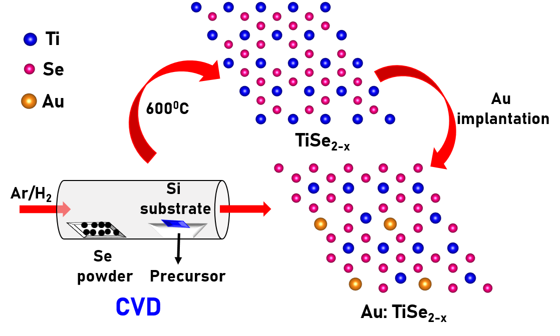
TiSe2-x nanocrystals with controlled Ti and Se raw ratio were grown on the Si substrates using a single zone Chemical Vapour Deposition (CVD) system in ambient pressure. Consistent and repeatable growth of hexagonal TiSe2-x nanocrystals on Si substrate was achieved using a modified version of the synthesis method provided by Wang et al [33]. The TiOx and LiCl mixture was kept at the centre of the CVD tube and maintained at 600∘C throughout the reaction. Se powder was kept upstream at a temperature of about 260∘C. Forming gas (mixture of H2 (5) and Ar (95)) was passed through the tube at 100 sccm. After synthesis, the samples were irradiated with 20 KeV Au ions at fluences of , , , and ions cm-2. The schematic of the setup along with the formation of TiSe2-x and Au defects in the matrix was illustrated in Fig. 1.
The phase identification of TiSe2-x samples, before and after Au ion implantation was carried out by Rigaku X-ray diffraction (XRD) using Cu-K radiation with a wavelength of = 1.5406Å. The surface morphology of as-deposited and Au-irradiated samples were characterized using Field Emission Scanning Electron Microscopy (FESEM) (Sigma-ZEISS). The elemental distribution of Ti, Se and Au was confirmed using an Energy Dispersive X-Ray Spectroscopy (EDXS) incorporated into the FESEM. We expect the formation of non functionalized Au nanoparticles in TiSe2-x with increasing fluence, which was later confirmed and visualized using High-Resolution Transmission Electron Microscopy (HR-TEM) micrographs with field emission electron source at 200 keV (Jeol-F200). Superconducting Quantum Interference Device (SQUID) magnetometry was used for magnetization measurement at all the temperatures ranging 5 K - 300 K.
III Results and Discussion
Grazing Incidence X-Ray Diffraction (GIXRD) measurements were performed to obtain information on TiSe2 formation, and track any changes after Au ion implantation.

Figure 2(a) shows the XRD pattern with peaks of (002), (003), and (110) planes as compared with the JCPDS file number 651885, within the 2 values of 25 to 55∘ corresponding to the crystal’s pm1 TiSe2 phase. The peaks at 2 values 41.35 and 43.6 correspond to the (110) and (012) planes of the residual Se on the substrates during CVD growth. All the peaks seem prominent, dominated by the (001) orientation; which confirms the formation of highly crystalline and oriented nanocrystals.
The calculated lattice parameters come out to be Å, and Å using the relation [34] for hexagonal TiSe2 crystal structure, which is in the ballpark for bulk TiSe2 [35]. The parameter “c” shows a slight decline with the fluence, however, the a and b values change quite significantly. This could be ascribed to the compressive strain along the a and b direction due to all the Se vacancy sites. All the TiSe2 peaks broaden as fluence is increased indicating the degradation of crystallinity. The inset in Fig. 2(a) shows the magnified version of the most prominent (002) peak. Crystalline size (D) and the dislocation density () were calculated using the Debye-Scherrer equation and the relation (=1/D2) [36] as a function of ion fluence, shown in Fig. 2(b). As expected, the mean crystalline size decreases from 36 nm to 18 nm as the ion fluence increases up to ions cm-2. We also see that the value increases from nm-2 to nm-2 as the ion fluence increases, shown in Fig. 2(b).
The surface morphology of the pristine and Au-irradiated TiSe2-x was studied using FESEM and EDXS. In FESEM images, we see the formation of hexagonal crystals, with length varying from 1 - 2 m as shown in Fig. 3. From cross-sectional FESEM, the thicknesses of the crystals is found to be in the range of 150 - 200 nm. The crystals progressively deform and become porous with the increase in ion fluences. A representative FESEM and EDXS mapping of fluence and ions cm-2 is shown in Fig. 3(b) and (c).
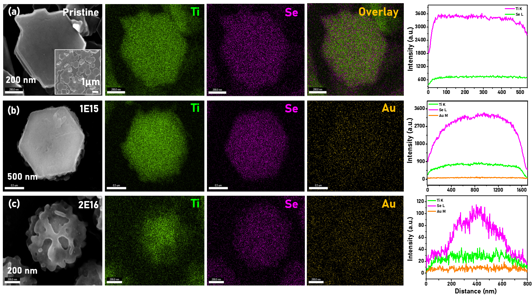
From elemental mapping, the distribution of Ti and Se mimic the hexagonal shape in all the samples, whereas Au is all over the surface area. The line scans demonstrate the uneven distribution of Ti, Se and Au after ion implantation. The Ti:Se ratio for the as-grown and implanted samples at different fluences are tabulated in Table 1. The calculated ratio of Ti/Se decreases as we go to higher fluences, which matches with our sputtering yield calculation using TRIDYN [Mller1984] and SRIM [37]. We see that the Ti:Se ratio systematically decreases with the increase in ion fluence, with the pristine standing at 1:1.80, decreasing to 1:1.73 and then to 1:1.09 as soon as the sample gets irradiated.
| Element | Pristine | 1 | 2 | 1 | 2 |
|---|---|---|---|---|---|
| Ti:Se | 1:1.8 | 1:1.7 | 1:1.6 | 1:1.2 | 1:1.1 |
| Au | - | 0.9 | 1.8 | 9.1 | 9.6 |
This is caused due to sputtering of Ti and Se ions as the high energy Au atoms strike the lattice at normal incidence. The atomic percentage of Au ions increases with fluence which is shown in Table 1. It is well known that the nuclear energy loss ( eV/nm) of 20 keV Au ions in TiSe2 yields a large amount of sputtering of Ti and Se atoms. The penetration depth of 20 keV Au is 20 nm (SRIM), extending till a depth of 30 nm, due to dynamic sputtering during ion implantation. The total calculated sputtering yield of Ti and Se are 6 atoms/ion, which is quite high to make TiSe2-x porous at high fluence.
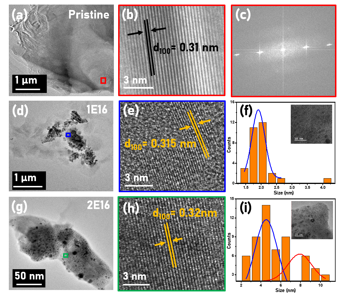
To characterize the effect of Au ion implantation on TiSe2-x nanocrystals, HRTEM analysis was performed. HRTEM images for the pristine and the samples irradiated at 1 and 2 ions cm-2 are shown in Fig. 4. For the TEM samples, some flakes of TiSe2-x were transferred from the Si surface onto the Cu TEM grid. Figure 4(a-c) shows the TEM micrograph, high-resolution fringe patterns (zoomed view of the red squared region), and corresponding Selected Area Diffraction Pattern (SAED) pattern of the pristine sample. It was observed that the fringes are oriented along the (100) plane and the calculated d value is 0.31 nm shown in Fig. 4(b). The Au ion implantation introduced defects and nanoscale amorphous regions and nanoparticles inside the TiSe2-x matrix. Structural distortion is visible in the 1 ions/cm2 irradiated sample, with a distinct increase in the lattice spacing to 0.315 nm (Fig. 4(e)) alongside the formation of small size Au nanoparticles as shown in the inset of Fig. 4(f). The particle size was calculated and the average domain size was determined to be 2 nm shown in Fig. 4(f). At the highest fluence of 2 ions cm-2 the lattice spacing increases to 0.32 nm (Fig. 4(h)) because of stress developed due to larger Se deficient in TiSe2-x. Due to heavy ion irradiation-induced self-heating, many small units agglomerate and tend to form larger Au nanoparticles as shown in the inset of Fig. 4(i). They show up as dark patches with nanoparticle sizes varying from 2 - 12 nm with a bimodal distribution. Two Gaussian fittings centred around 5 nm and 8 nm are the average size of the Au nanoparticles shown in Fig. 4(i).
Ferromagnetic behaviour in TiSe2 is especially astounding because the Ti atoms are hybridized with Se atoms by covalent Ti–Se interaction, which quenches the magnetic moment keeping it non-magnetic. Most of the reports on ferromagnetism in TiSe2 have been studied through several ways: (a) Via introducing magnetic atoms leading to magnetism or spin polarization [31], (b) By way of incorporating single Se-anion defects and intercalating Ti atoms inside the TiSe1.8 material [12], (c) By using secondary phases [38]. Tong et al [12] demonstrated that TiSe1.8 is ferromagnetic with local magnetic moments and spin polarization due to single Se-cation and Ti intercalation. But in our case, the pristine sample has intrinsic Se defects, showing up in the form of TiSe2-x, which varies with Au incorporation. So exploring the tunable magnetic properties by an effective strategy to induce and control the ferromagnetism is highly desirable. The incorporation of Au atoms by low energy ion implantation was used as a regulating knob to control the Se vacancies, Au intercalation and Ti intercalation in order to trigger the magnetic ordering.
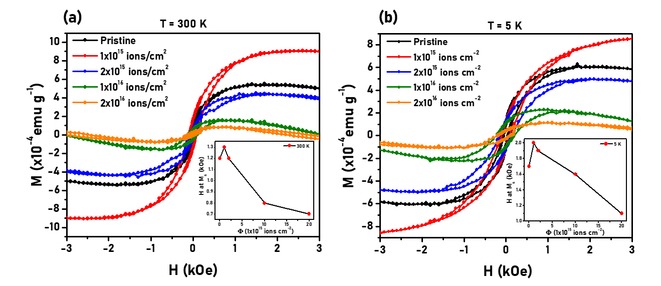
Figure 5(a) and (b) show the ferromagnetic response of the as-deposited and the post irradiated samples at 300 K and 5 K, respectively with different ion fluences in the range of 1- 2 ions cm-2. It was noticed that the as-prepared TiSe1.8 system illustrates a characteristic ferromagnetic S-shaped (M-H) curve. In contrast, diamagnetic behaviour starts showing up with the increase in ion fluence. As the temperature decreases from 300 K to 5 K, the width of the hysteresis loop becomes more prominent for all samples. In all temperature ranges, we observed a sharp increase in the saturation magnetisation at the lowest fluence and a steady decrease from thereon. The magnetic moment saturates faster with increasing ion fluence. The insets of Fig. 5 (a) and (b) show the behaviours of the applied magnetic field for Ms as a function of ion fluence. Both at 300 K and 5 K the magnetic field at Ms increases for the lowest fluence, then decreases as a function of ion fluence. A similar trend was observed for all the temperatures. During ion implantation, both Se and Ti atoms get sputtered out, which creates more Se vacancies, Ti displacements, and Au incorporation. Such synergistic effect creates controllable defect states, eventually reducing the total magnetic moment per unit volume, requiring less applied magnetic field for saturation magnetization at higher fluence.
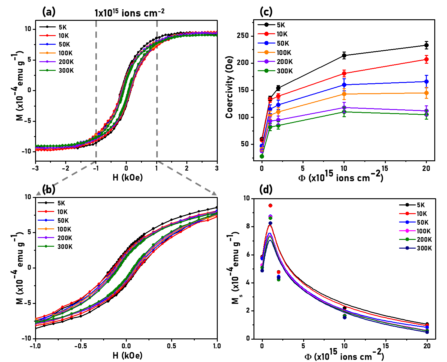
A representative plot with a complete systematic study of the S-shaped hysteresis loop in a temperature range of 5 K to 300 K at a fluence of 1 ions cm-2 is depicted in Fig. 6(a). Magnified view of the relevant region in the applied magnetic field of -1000 Oe to 1000 Oe is shown in Fig. 6(b). With the increase in temperature, the hysteresis width decreases, resulting in a decrease in its coercivity. The coercivity and saturation magnetisation (Ms) values were extracted from the M-H curve for as-deposited and post irradiated samples for all the variable temperatures and displayed in Fig. 6(c) and (d). The coercivity values of the samples increase with ion fluence at all the temperatures as shown in Fig. 6(c). The maximum change of coercivity observed is from 45 Oe to 235 Oe at 5 K, whereas the change is from 40 to 75 Oe at 300 K. In Fig. 6(d), we have observed that the Ms value seems to bump up at a fluence of 1 ions cm-2 and then decrease as we increase the ion fluence.
It is observed from the hysteresis loop of Fig. 5(a) and (b) that the diamagnetic contribution becomes higher with the decrease in saturation magnetisation. In this work, we show that competing contributions between ferromagnetic (FM) and diamagnetic (DM) phases result in opposite effects: enhancement of coercivity and decrease in the saturation magnetisation. The source of FM and diamagnetic dip can be explained by all the different oxidation states from the different atoms present in the matrix. Since we are bombarding Au atoms on Se deficient samples, we expect the presence of mixed oxidation states from Titanium, which is Ti3+, Ti4+[12], and Au3+. To explain the coexistence of FM and DM phases, we resort to the modified Brillouin function [39]. The positive arms of the M-H curves were fitted using the Brillouin J relation to calculate the magnetization theoretically using the triplets of atoms contributing to magnetization. The following Brillouin function was used which takes into account the contribution of both FM and DM phases.
| (1) |
Where Msat is the saturation magnetization, and the Brillouin J function is defined with as:
| (2) | |||||
| (3) |
where
| (4) | |||||
| (5) |
and is defined as:
| (6) |
represents the effective magnetic susceptibility; its value is negative for DM contributions and positive in case of a FM one. It should be noted that the linear correction would correct for diamagnetic tendencies in the sample, which is observed at the farther edge of the hysteresis curves [39] in Fig. 7.
The fitting of Brillouin J function with the values corresponding to Ti3+’s of the as-grown sample without any diamagnetic correction term is shown in Fig. 7(a), as the M-H hysteresis curve shows ferromagnetic behaviour and has no prior reports suggesting diamagnetism in pristine systems. Tong et al [12] demonstrate that the intrinsic local magnetic moments arise from Ti3+’s 3d1 electron configuration in TiSe1.8. Figure 7(b) and (c) show the fits for the Au implanted samples at a fluence of 1 ions cm-2 and 2 ions cm-2 respectively. The fits seem to stay within the experimental error (filled area) in the measurement of magnetization for all the samples shown in Fig. 7(a-c). The two parts of the Brillouin function correspond to the contribution by Au3+’s state along with Ti3+’s with a diamagnetic correction term stemming from the Au implantation [38, 40, 41]. We don’t fit for the Au’s state here, because it corresponds to d0, which doesn’t give us a definite triplet. One can see that the diamagnetic contribution increases as the fluence increases (Fig. 7(c)).
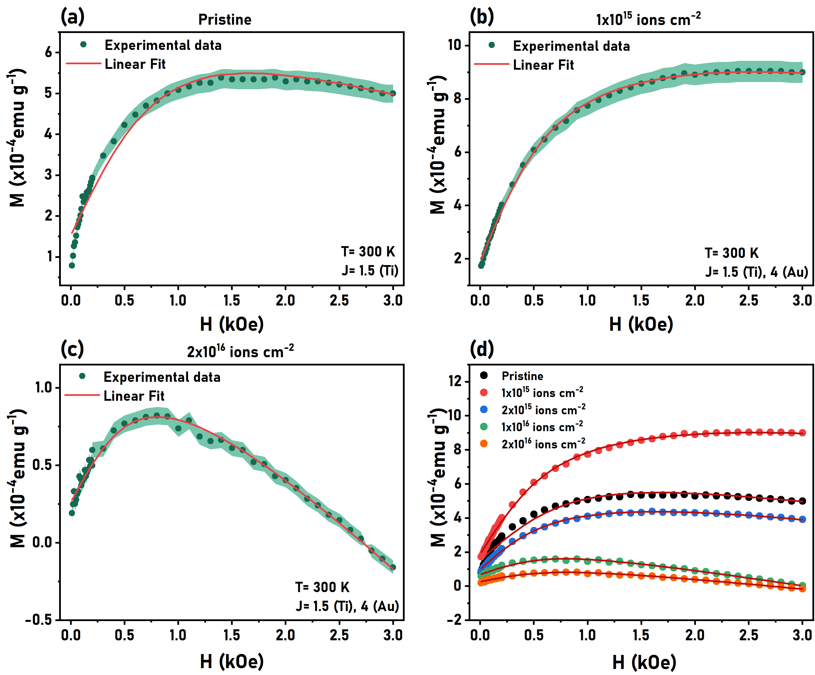
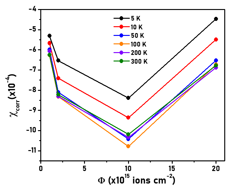
Figure 8 shows the correction () factor for the Au implanted samples at different fluences calculated from the fits. The value of is negative due to the diamagnetic behaviour, with the magnitude increasing systematically till 1 ions cm-2, then dropping sharply at the highest fluence of 2 ions cm-2, which is attributed as the formation of a high number of non-magnetic Au agglomerates.
It was observed that at all the temperatures, Ms shows a sharp increase at lower fluences, and then a systematic decline as the fluence goes higher. To explain such an effect, we have modelled the modification of the TiSe2 matrix by Au ion incorporation as illustrated in Fig. 9. It is very clear that the Ti3+ states created due to the Se deficiency is the source of magnetization in case of the pristine TiSe1.8 sample [12, 42]. Figure 9 (a) shows a model for Se deficient pristine samples where the Ti3+ states have a net magnetic moment. We have explored an approach to effectively control the magnetization by introducing Au ions, which can prompt magnetization in non-magnetic materials depending on the nanoparticle size. Li et al [41] have shown us that the magnetic properties of Au nanoparticles are most pronounced when they are at around 2 - 4 nm in size. At lower fluences, the Au atoms are randomly distributed. At the same time, some of the Se and Ti atoms are knocked out due to ion beam sputtering. The calculated sputtering yield of Ti and Se at a fluence of ions cm-2 is 1.7 and 4.3 atoms/ion respectively. Since the sputtering yield of Ti is lesser as compared to Se, the probability of Ti3+ formation is high because the excess Se vacancies would transfer one electron to the empty 3d orbital of Ti atoms. At the same time, Au atoms are distributed randomly all over the area of irradiation, creating Au nanoparticles in the matrix. Figure 9(b) shows the model for Ti3+ and distributed Au3+ sample at a lower fluence. HRTEM micrographs with the Au nanoparticle distribution in Fig. 4(f) seem to agree with our model. These combined factors provide us with a good explanation for the higher saturation magnetization at a fluence of 1 ions cm-2 compared to the as grown sample.
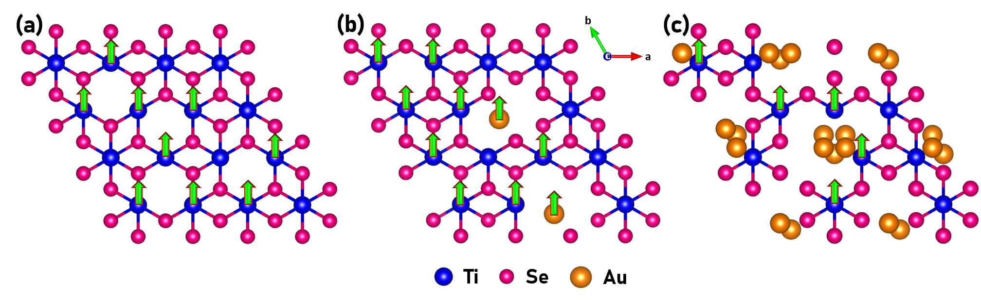
A decrease in Ms was observed with an increase in ion fluences. This may be due to the decrease in the net volume concentration of atoms contributing to magnetization. As the fluence increases the sputtering yield goes up for Ti atoms and down for Se atoms. At higher fluences (2 ions cm-2), the sputtering yield is 1.9 and 4.2 atoms/ion for Ti and Se respectively. This yield increases porosity in TiSe1.8 thin films as shown in Fig. 3(c) in the FESEM image, which is the major reason for the decline in magnetization. At this fluence, Ms goes down to a minimum because (a) Volume concentration of Ti3+ decreases due to sputtering out of a large fraction of Ti atoms, (b) Au ions agglomerate into nanoclusters with an average size of 4 - 8 nm (as shown in Fig. 4(i) of HRTEM image), which increase the DM contribution and decrease the magnetization. Figure 9(c) illustrates the clustering stage of the sample. The systematic increase in the diamagnetic behaviour stems from Au nanoparticles sitting within the lattice. It is clear that by engineering defects via precise Au ion incorporation, one can indeed control ferromagnetism in TiSe2.
IV Conclusion
We have demonstrated that the ferromagnetic order can be tuned in CVD grown 2D TiSe1.8 TMDs by 20 keV Au ion implantation. The structural changes and stoichiometric variations of Ti and Se after Au incorporation were confirmed from XRD, FESEM with EDXS, and HRTEM. The intrinsic ferromagnetism in TiSe1.8 arises from the Ti3+ oxidation state generated by Se vacancies. Depending on the ion fluence, the system became disordered by the introduction of Au nanoparticles and nanoclusters. When the Au nanoparticle size remained within 2 - 4 nm, the system showed ferromagnetism dominantly. Larger Au nanoparticles increased the diamagnetic contribution. At the highest fluence, TiSe1.8 matrix turned porous with a high dislocation density, and Au nanoclusters went on to reduce the FM contribution and enhance the DM contribution. The DM contributions () were estimated by fitting the hysteresis curve using a modified Brillouin function incorporating both the Ti3+ and Au3+ oxidation states with J values of 1.5 and 4, respectively. Precise Au incorporation with a balanced FM and DM contribution can pave a new way to tune layered TMD materials’ magnetic properties and shine new light on their potential applications in spintronic and magnetic sensing devices.
Acknowledgments
This work was supported by National Institute of Science Education and Research, DAE, India. The authors acknowledge the staff of low energy ion beam facility of Institute of Physics (IOP), Bhubaneswar for providing stable beams during ion implantation. PKS thanks Dr. Kartik Senapati for fruitful scientific discussion.
References
- Guo et al. [2019] S. Guo, Y. Zhang, Y. Ge, S. Zhang, H. Zeng, and H. Zhang, 2d v-v binary materials: Status and challenges, Advanced Materials 31, 1902352 (2019).
- Baek and Kim [2017] D.-H. Baek and J. Kim, MoS 2 gas sensor functionalized by pd for the detection of hydrogen, Sensors and Actuators B: Chemical 250, 686 (2017).
- Pan et al. [2020] W. Pan, Y. Zhang, and D. Zhang, Self-assembly fabrication of titanium dioxide nanospheres-decorated tungsten diselenide hexagonal nanosheets for ethanol gas sensing application, Applied Surface Science 527, 146781 (2020).
- Lopez-Sanchez et al. [2013] O. Lopez-Sanchez, D. Lembke, M. Kayci, A. Radenovic, and A. Kis, Ultrasensitive photodetectors based on monolayer MoS2, Nature Nanotechnology 8, 497 (2013).
- Fiori et al. [2014] G. Fiori, F. Bonaccorso, G. Iannaccone, T. Palacios, D. Neumaier, A. Seabaugh, S. K. Banerjee, and L. Colombo, Electronics based on two-dimensional materials, Nature Nanotechnology 9, 768 (2014).
- Jariwala et al. [2014] D. Jariwala, V. K. Sangwan, L. J. Lauhon, T. J. Marks, and M. C. Hersam, Emerging device applications for semiconducting two-dimensional transition metal dichalcogenides, ACS Nano 8, 1102 (2014).
- Chen et al. [2017] X. Chen, G. Liu, Y. Hu, W. Cao, P. Hu, and W. Hu, Vertical MoSe2–MoO x p–n heterojunction and its application in optoelectronics, Nanotechnology 29, 045202 (2017).
- Jiang et al. [2020] X. Jiang, A. V. Kuklin, A. Baev, Y. Ge, H. Ågren, H. Zhang, and P. N. Prasad, Two-dimensional MXenes: From morphological to optical, electric, and magnetic properties and applications, Physics Reports 848, 1 (2020).
- Guo et al. [2014] Y. Guo, J. Dai, J. Zhao, C. Wu, D. Li, L. Zhang, W. Ning, M. Tian, X. C. Zeng, and Y. Xie, Large negative magnetoresistance induced by anionic solid solutions in two-dimensional spin-frustrated transition metal chalcogenides, Physical Review Letters 113, 157202 (2014).
- Zhu et al. [2016] X. Zhu, Y. Guo, H. Cheng, J. Dai, X. An, J. Zhao, K. Tian, S. Wei, X. C. Zeng, C. Wu, and Y. Xie, Signature of coexistence of superconductivity and ferromagnetism in two-dimensional NbSe2 triggered by surface molecular adsorption, Nature Communications 7, 11210 (2016).
- Ma et al. [2012] Y. Ma, Y. Dai, M. Guo, C. Niu, Y. Zhu, and B. Huang, Evidence of the existence of magnetism in pristine VX2 monolayers (x = s, se) and their strain-induced tunable magnetic properties, ACS Nano 6, 1695 (2012).
- Tong et al. [2017] Y. Tong, Y. Guo, K. Mu, H. Shan, J. Dai, Y. Liu, Z. Sun, A. Zhao, X. C. Zeng, C. Wu, and Y. Xie, Half-metallic behavior in 2d transition metal dichalcogenides nanosheets by dual-native-defects engineering, Advanced Materials 29, 1703123 (2017).
- Ahmed et al. [2020] S. Ahmed, X.-Y. C. Cui, X. Ding, P. P. Murmu, N. Bao, X. Geng, S. Xi, R. Liu, J. Kennedy, T. Wu, L. Wang, K. Suzuki, J. Ding, X. Chu, S. R. C. Indirathankam, M. Peng, A. Vinu, S. P. Ringer, and J. Yi, Colossal magnetization and giant coercivity in ion-implanted (nb and co) MoS2 crystals, ACS Applied Materials & Interfaces 12, 58140 (2020).
- Ahmed et al. [2019] S. Ahmed, X. Ding, P. P. Murmu, N. Bao, R. Liu, J. Kennedy, L. Wang, J. Ding, T. Wu, A. Vinu, and J. Yi, High coercivity and magnetization in WSe 2 by codoping co and nb, Small 16, 1903173 (2019).
- Zhang et al. [2014] W. Zhang, Z. Huang, W. Zhang, and Y. Li, Two-dimensional semiconductors with possible high room temperature mobility, Nano Research 7, 1731 (2014).
- Wei et al. [2017] M. J. Wei, W. J. Lu, R. C. Xiao, H. Y. Lv, P. Tong, W. H. Song, and Y. P. Sun, Manipulating charge density wave order in monolayer 1t-TiSe2 by strain and charge doping: A first-principles investigation, Physical Review B 96, 165404 (2017).
- Goli et al. [2012] P. Goli, J. Khan, D. Wickramaratne, R. K. Lake, and A. A. Balandin, Charge density waves in exfoliated films of van der waals materials: Evolution of raman spectrum in TiSe2, Nano Letters 12, 5941 (2012).
- Monney et al. [2015] G. Monney, C. Monney, B. Hildebrand, P. Aebi, and H. Beck, Impact of electron-hole correlations on the1t-TiSe2electronic structure, Physical Review Letters 114, 086402 (2015).
- Ozaydin et al. [2015] H. D. Ozaydin, H. Sahin, J. Kang, F. M. Peeters, and R. T. Senger, Electronic and magnetic properties of 1 t-TiSe 2 nanoribbons, 2D Materials 2, 044002 (2015).
- Kaur et al. [2017] H. Kaur, S. Yadav, A. K. Srivastava, N. Singh, S. Rath, J. J. Schneider, O. P. Sinha, and R. Srivastava, High-yield synthesis and liquid-exfoliation of two-dimensional belt-like hafnium disulphide, Nano Research 11, 343 (2017).
- Eda et al. [2011] G. Eda, H. Yamaguchi, D. Voiry, T. Fujita, M. Chen, and M. Chhowalla, Photoluminescence from chemically exfoliated MoS2, Nano Letters 11, 5111 (2011).
- Cai et al. [2015] L. Cai, J. He, Q. Liu, T. Yao, L. Chen, W. Yan, F. Hu, Y. Jiang, Y. Zhao, T. Hu, Z. Sun, and S. Wei, Vacancy-induced ferromagnetism of MoS2 nanosheets, Journal of the American Chemical Society 137, 2622 (2015).
- Salvo et al. [1976] F. J. D. Salvo, D. E. Moncton, and J. V. Waszczak, Electronic properties and superlattice formation in the semimetalTiSe2, Physical Review B 14, 4321 (1976).
- Rossnagel [2011] K. Rossnagel, On the origin of charge-density waves in select layered transition-metal dichalcogenides, Journal of Physics: Condensed Matter 23, 213001 (2011).
- Holt et al. [2001] M. Holt, P. Zschack, H. Hong, M. Y. Chou, and T.-C. Chiang, X-ray studies of phonon softening inTiSe2, Physical Review Letters 86, 3799 (2001).
- Xi et al. [2015] X. Xi, L. Zhao, Z. Wang, H. Berger, L. Forró, J. Shan, and K. F. Mak, Strongly enhanced charge-density-wave order in monolayer NbSe2, Nature Nanotechnology 10, 765 (2015).
- Joe et al. [2014] Y. I. Joe, X. M. Chen, P. Ghaemi, K. D. Finkelstein, G. A. de la Peña, Y. Gan, J. C. T. Lee, S. Yuan, J. Geck, G. J. MacDougall, T. C. Chiang, S. L. Cooper, E. Fradkin, and P. Abbamonte, Emergence of charge density wave domain walls above the superconducting dome in 1t-TiSe2, Nature Physics 10, 421 (2014).
- Calandra [2015] M. Calandra, Charge density waves go nano, Nature Nanotechnology 10, 737 (2015).
- Li et al. [2019] P. Li, X. Zheng, H. Yu, G. Zhao, J. Shu, X. Xu, W. Sun, and S. X. Dou, Electrochemical potassium/lithium-ion intercalation into TiSe2: Kinetics and mechanism, Energy Storage Materials 16, 512 (2019).
- Yan et al. [2018] B. Yan, B. Zhang, H. Nie, G. Li, X. Sun, Y. Wang, J. Liu, B. Shi, S. Liu, and J. He, Broadband 1t-titanium selenide-based saturable absorbers for solid-state bulk lasers, Nanoscale 10, 20171 (2018).
- Luo et al. [2015] H. Luo, J. W. Krizan, E. M. Seibel, W. Xie, G. S. Sahasrabudhe, S. L. Bergman, B. F. Phelan, J. Tao, Z. Wang, J. Zhang, and R. J. Cava, Cr-doped TiSe2 – a layered dichalcogenide spin glass, Chemistry of Materials 27, 6810 (2015).
- Morosan et al. [2006] E. Morosan, H. W. Zandbergen, B. S. Dennis, J. W. G. Bos, Y. Onose, T. Klimczuk, A. P. Ramirez, N. P. Ong, and R. J. Cava, Superconductivity in CuxTiSe2, Nature Physics 2, 544 (2006).
- Wang et al. [2018] H. Wang, Y. Chen, M. Duchamp, Q. Zeng, X. Wang, S. H. Tsang, H. Li, L. Jing, T. Yu, E. H. T. Teo, and Z. Liu, Large-area atomic layers of the charge-density-wave conductor TiSe2, Advanced Materials 30, 1704382 (2018).
- Bindu and Thomas [2014] P. Bindu and S. Thomas, Estimation of lattice strain in ZnO nanoparticles: X-ray peak profile analysis, Journal of Theoretical and Applied Physics 8, 123 (2014).
- P et al. [2019] B. P, B. Sumit, P. M. M, and G. V, Cdw transition in fe intercalated tise2, AIP Conference Proceedings 2100, 020113 (2019).
- Kumar et al. [2017] P. Kumar, P. Kumar, A. Kumar, I. Sulania, F. Chand, and K. Asokan, Structural, optical and magnetic properties of n ion implanted CeO2 thin films, RSC Advances 7, 9160 (2017).
- Ziegler et al. [2010] J. F. Ziegler, M. Ziegler, and J. Biersack, SRIM – the stopping and range of ions in matter (2010), Nuclear Instruments and Methods in Physics Research Section B: Beam Interactions with Materials and Atoms 268, 1818 (2010).
- Prusty et al. [2016] S. Prusty, V. Siva, N. Shukla, B. Satpati, K. Senapati, and P. K. Sahoo, Unusual ferromagnetic behaviour of embedded non-functionalized au nanoparticles in bi/au bilayer films, RSC Advances 6, 106584 (2016).
- Es-saddik et al. [2020] F. Es-saddik, K. Limame, S. Sayouri, M. Hamzah, M. Khenfouch, and V. V. Srinivasu, Magnetic properties of sm-doped barium titanate (ba0.99sm0.01tio3) prepared by sol–gel route, Journal of Materials Science: Materials in Electronics 31, 19910 (2020).
- Hori et al. [2004] H. Hori, Y. Yamamoto, T. Iwamoto, T. Miura, T. Teranishi, and M. Miyake, Diameter dependence of ferromagnetic spin moment in au nanocrystals, Phys. Rev. B 69, 174411 (2004).
- Li et al. [2011] C.-Y. Li, C.-M. Wu, S. K. Karna, C.-W. Wang, D. Hsu, C.-J. Wang, and W.-H. Li, Intrinsic magnetic moments of gold nanoparticles, Physical Review B 83, 174446 (2011).
- Xiao et al. [2019] Y. Xiao, M. Zhou, M. Zeng, and L. Fu, Atomic-scale structural modification of 2d materials, Advanced Science 6, 1801501 (2019).