THz radiation induced circular Hall effect in graphene
Abstract
We report on the observation of the circular transversal terahertz photoconductivity in monolayer graphene supplied by a back gate. The photoconductivity response is caused by the free carrier absorption and reverses its sign upon switching the radiation helicity. The observed dc Hall effect manifests the time inversion symmetry breaking induced by circularly polarized terahertz radiation in the absence of a magnetic field. For low gate voltages, the photosignal is found to be proportional to the radiation intensity and can be ascribed to the alignment of electron momenta by the combined action of THz and static electric fields as well as by the dynamic heating and cooling of the electron gas. Strikingly, at high gate voltages, we observe that the linear-in-intensity Hall photoconductivity vanishes; the photoresponse at low intensities becomes superlinear and varies with the square of the radiation intensity. We attribute this behavior to the interplay of the second- and fourth-order effects in the radiation electric field which has not been addressed theoretically so far and requires additional studies.
I Introduction
Optoelectronic phenomena in graphene, providing a highly effective means for the manipulation and control of carriers by radiation from the visible to terahertz (THz) frequency range, are subject of enormous current interest, see e.g. [1, 2, 3, 4, 5, 6, 7, 8, 9, 10, 11, 12, 13, 14, 15, 16, 17, 18]. In the last decade it was demonstrated that a circularly polarized radiation can produce a dc electric current whose direction and magnitude are controlled by the radiation helicity, see e.g. [19, 20, 21, 22, 23, 24, 11, 25, 26, 27, 28, 29, 30, 31, 32, 33, 34]. A particularly intriguing phenomenon is the circular Hall effect arising in the absence of static magnetic fields. The Hall current can appear either in unbiased samples, where it is driven by the crossed electric and magnetic fields of a circularly polarized wave and is termed the dynamic circular Hall effect [20, 22, 24, 11, 25, 26], or as circular transverse photoconductivity in the presence of a dc current, where it is driven solely by the electric field of the wave and is also termed the photovoltaic Hall effect [19, 23, 27, 28, 34]. At low intensity of illumination, the lowest-order transverse photoconductivity has two contributions, one coming from the optical alignment of electron momenta and the other from the dynamic heating and cooling of the electron gas [34]. In addition, a high-intensity circularly polarized light can open gaps in the Dirac spectrum, which, as predicted in Ref. [19] and recently demonstrated by applying mid-infrared radiation in Ref. [27], also leads to a photoinduced dc Hall current governed by the direct interband couplings. For highly doped samples and/or for terahertz radiation with relatively small photon energies not exceeding several meV, the spectrum reconstruction effects [19] driven by the interband couplings should be less pronounced. In this case, the intraband free carrier absorption [34] is expected to dominate the circular Hall effect in photoconductivity.
Here we report an observation and study of the circular transverse photoconductivity in graphene induced by terahertz radiation of moderate and large intensity. We demonstrate that absorption of the terahertz radiation results in a Hall photocurrent whose direction changes to the opposite with inversion of either the bias voltage polarity or the radiation helicity. The detected Hall photoresponse is negligibly small at the charge neutrality point (CNP). At low gate voltages away from the CNP, the photoresponse is proportional to the radiation intensity at low intensities sometimes saturating at higher . Such behavior is consistent with theory predicting the circular transverse photoconductivity of second order in the radiation electric field , see Refs. [35, 19, 34]. Strikingly, at high electron densities corresponding to higher gate voltages, the observed Hall photosignals exhibit a superlinear intensity dependence and vary as . Such behavior is detected for several frequencies ranging from 0.78 to 3.33 THz. Unlike the transverse photoconductivity, the longitudinal photoconductivity signal measured parallel to the bias current was insensitive to the radiation helicity. We discuss the observed THz radiation-induced circular Hall effect in terms of intraband electron kinetics in the presence of static and circular high-frequency electric fields. The corresponding quasiclassical theory [34] is consistent with our experimental results at low gate voltages and clarifies why the linear-in- contributions show up away from the CNP and can drop down at high gate voltages. An extension of this theory to higher orders is required to explain the emergence of strong quadratic-in- contributions to the circular Hall effect dominating the observed THz photosignals at high gate voltages and high intensities.
II Samples and methods
The exfoliated graphene/hexagonal boron nitride stacks [36, 37, 38] were prepared as Hall bar structures, see the microscope picture of sample #A in Fig. 1 (a). All investigated samples #A, #B, and #C had a Hall bar width of m and length of m and manifested similar transport- and photoresponce. By changing the back gate voltage the carrier density could be tuned in a wide range and varied symmetrically with the effective gate voltage, , as , where and are electron and hole sheet densities at positive and negative , respectively. Here was determined separately for every cool down tracing slight shifts of the gate voltage corresponding to the charge neutrality point (CNP). Figure 1 (c) depicts the carrier density obtained from classical Hall measurements at liquid helium temperature in the absence of THz illumination. For these measurements an ac current of 10 nA at a frequency of Hz was applied to the sample. The corresponding Fermi level position as a function of is presented in Fig. 1 (d). It was calculated using the conventional relations , and a standard value cm/s for the electron velocity in graphene.
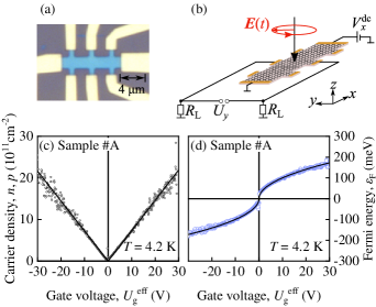
For studies of the circular Hall effect we used a high power pulsed THz molecular gas laser [39, 40, 41] pumped by a transversely excited atmospheric pressure (TEA) CO2 laser [42]. As illustrated in Fig. 1 (b) the sample was illuminated with circularly polarized THz pulses at normal incidence. The laser operated at frequencies and with pulse duration of about 100 ns and repetition rate of 1 Hz. The laser power, analyzed by photon drag detectors, was of the order of tens of kW varying for different frequencies. Taking into account the diameter of the Gaussian beam profile (1.5-3 mm), known from measurements using a pyroelectric camera, intensities up to 150 kW/cm2 could be achieved on the sample position. To control the laser radiation intensity arriving on the sample we placed two grid polarizers into the optical path, where the first one was rotatable and the second one was at a fixed position [43, 32]. The radiation polarization was modified by placing -plates in front of the sample, which were rotated by an angle between the axis of the plate and the electric field vector of the laser radiation after the second grid polarizer. In most of the experiments we used angles and corresponding to the right handed () and left handed () circularly polarized light, respectively. The sample was placed into an optical temperature-regulated continuous flow cryostat where it was cooled down to K. The -cut crystal quartz windows were covered by a black polyethylene film transparent for THz radiation preventing the undesired illumination of the sample with room light.
To change the sample conductivity under THz illumination a dc bias voltage was applied between source and drain contacts, i.e. along the long side of the Hall bar (direction) 111Note that few final measurements were carried out for applied between contacts neighboring the damaged source and drain contacts, which had no apparent effect on the signal recorded for the Hall voltage induced in the middle of the Hall bar.. The transverse (Hall) photosignal was picked up between two oppositely placed contacts at the middle of the Hall bar and measured as a voltage drop over load resistors , see Fig. 1(b). For comparison, we also studied the longitudinal photoconductivity within the two-terminal measurement scheme in which a voltage drop or was measured between two contacts biased over a load resistor either across the Hall bar (Fig. 2 in the main text) or along the Hall bar (Fig. 8 in the supplementary materials).
III Results
Measurements under circularly polarized radiation revealed the helicity-sensitive Hall photoresponse. It was detected in direction across the Hall bar perpendicular to the direction of the applied bias voltage . Figure 2(a) shows a typical bias voltage dependence of the photoresponse to right-handed () and left-handed () circularly polarized radiation. It demonstrates that for fixed radiation helicity the signal is proportional to the applied bias voltage. It vanishes at zero bias voltage, and changes the sign by switching from negative to positive . These facts reveal that the main signal comes from the change of the sample conductivity. We also observed that the variation of the signal with bias voltage remained linear for up to V, with a tendency to saturate at higher bias voltages, see Fig. 2(a).
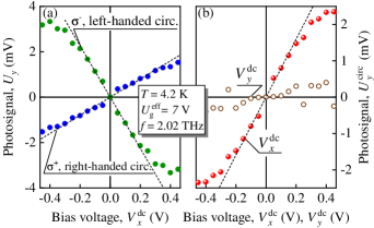
Importantly, an inversion of the radiation helicity consistently inverted the sign of the Hall photoconductivity signal, see Fig. 2(a). Rotating the -plate we observed that the signal closely follows the degree of circular polarization so that (not shown). Here, and are intensities of the right- and left-handed circularly polarized radiation. We emphasize that such a helicity sensitive behaviour was only observed for the Hall photoconductivity, i.e. for detected with the dc bias applied along the Hall bar. For longitudinal photoconductivity, in contrast, the signals for right and left handed circular polarization were almost identical, see Fig. 8 in the supplementary materials. To explore the functional behavior of the helicity dependent signal, we write it as
| (1) |
where and are the photosignals generated by right- and left-handed circularly polarisation, respectively. The variation of the Hall circular photoresponse with bias voltage is shown in Fig. 2(b) together with the results of the longitudinal circular photoresponse obtained for the bias voltage applied in direction. The circular longitudinal signal is almost zero, see Fig. 2(b) and Fig. 8 in the supplementary materials, and, similar to the Hall signal, changes its sign upon inversion of the bias voltage polarity.
While the sign change upon switching the bias voltage polarity was detected in all measurements, the magnitude of signals for and were slightly different, see Fig. 2(a) and Fig. 7 in the supplementary materials. This observation is attributed to the generation of the photogalvanic currents [11, 32]. Using that, by definition, the linear-in- photoconductivity signal should have opposite sign for positive and negative bias voltages whereas the the photogalvanic current should be insensitive to the polarity of , we extracted the photoconductivity contribution as an odd part of ,
| (2) |
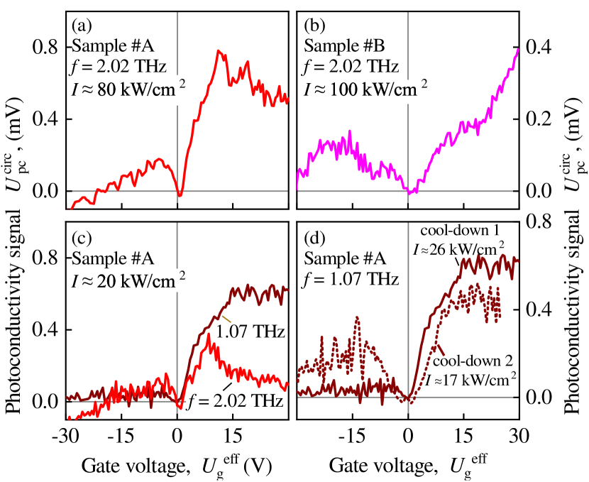
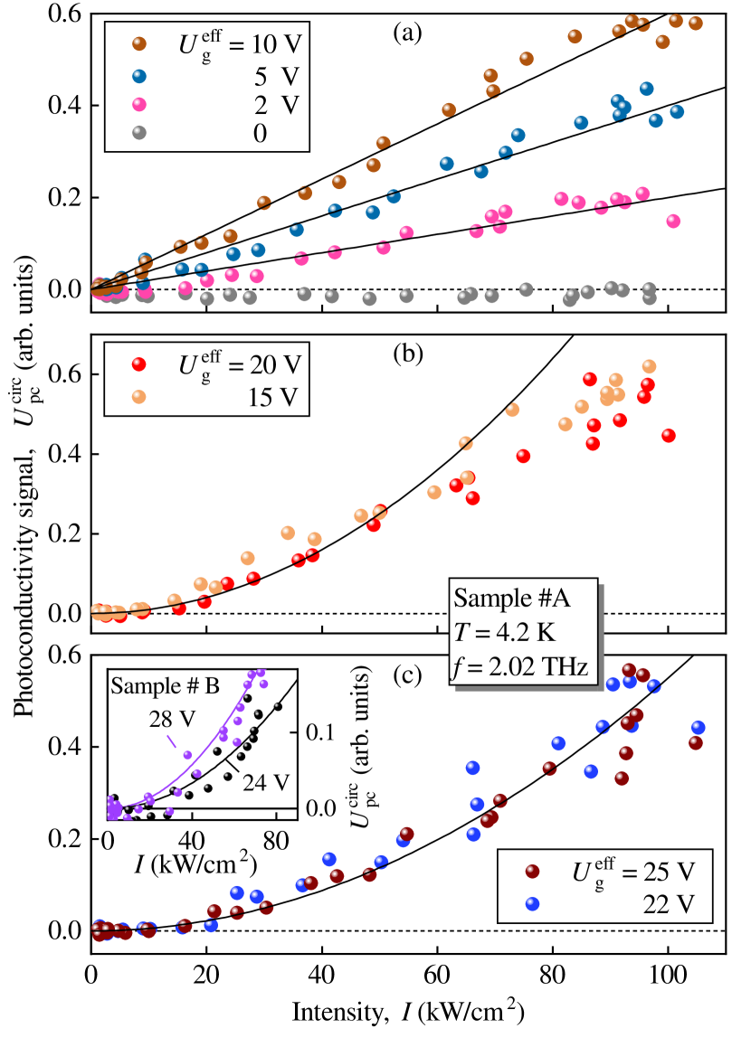
Figure 3 illustrates the gate voltage dependence of the corresponding circular photoconductivity signal . Panels (a) and (b) show obtained in samples #A and #B under intense THz radiation with kW/cm-2. These traces demonstrate that the circular photoconductivity is negligible at the CNP, and, for small gate voltages, increases almost linearly and symmetrically with . At higher gate voltages, however, the dependences become asymmetric: for positive gate voltages increases further and typically saturates at high gate voltages, whereas for the negative the Hall photoconductivity decreases and may even change the sign. Similar results are obtained for lower intensities and other frequencies, see Fig. 3(c). The electron-hole asymmetry of the circular photoconductivity was detected in all measurements, but was different for different cool downs. Figure 3(d) shows an exemplary gate voltage dependence of the signal obtained for two different cool downs. While for positive gate voltages both amplitude and functional behavior are similar, for negative gate voltages in one of the cool downs the signal is close to zero for all . Therefore, in the following we focus on the data obtained for positive gate voltages.
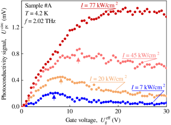
Figure 4 shows the gate voltage dependences obtained for THz with different radiation intensities. It demonstrates that the circular photoconductivity depends non-monotonically on : at low intensities it increases almost linearly with raising , reaches a maximum and decreases for large . The maximum position depends on the radiation intensity and shifts to higher with increasing radiation intensity.
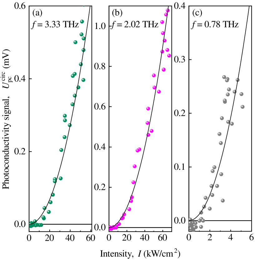
While for low gate voltages the circular photoconductivity linearly increases with increasing radiation intensity , see Fig. 5, or saturates at high (not shown), at high gate voltages it becomes superlinear. In the latter case, in particular, for the highest gate voltages, the data can be well fitted by , where is a fit parameter, see Fig. 5(b) and (c) for sample #A and the inset in Fig. 5(c) for sample #B. The superlinearity at high gate voltages has been detected for all radiation frequencies, see Fig. 6. The coefficients increase at low frequency, for instance, . Note that in our laser systems the highest available intensities become lower at low radiation frequencies, see Fig. 6.
IV Discussion
We begin the discussion of the observed circular photoconductivity by reviewing the results of a phenomenological theory based on general symmetry arguments. When an isotropic system is excited by normally incident spatially homogeneous terahertz radiation, the minimal order dc photocurrent, linear with respect to the dc electric field applied in direction and quadratic in the radiation electric field , is fully characterised [35] by three transport coefficients ,
| (3) | ||||
| (4) |
where , , and are Stokes parameters describing the polarization of the radiation field. In the case of circular polarization, the anisotropic terms proportional to vanish, and the photoresponce is reduced to
| (5) | ||||
| (6) |
where the helicity represents the two possible values of for right- and left-handed circular polarization. The form of the photoresponse given by Eq. (6) is analogous to the conventional Hall effect, with the circularly polarized radiation playing the role of the time reversal symmetry breaking field instead of magnetic field and with the diagonal and Hall components of the photoconductivity tensor being even and odd with respect to the helicity , in accord with our observations, see Figs. 2, 3, 4, and 6 for the Hall photocurrent, and Figs. 2(b) and 8 for the longitudinal photocurrent. Note that in Fig. 2(b) the longitudinal current was detected by applying the bias voltage across the Hall bar, along direction, and by measuring the corresponding component of the photocurrent.
In general, the photoconductivity response to THz radiation may be caused by either direct interband or indirect intraband optical transitions, the latter being due to the scattering-assisted free carrier absorption. In degenerate graphene at low temperatures, the interband processes require photon energies larger than twice the Fermi energy since the final states for optical transition should be free. Thus the interband photoconductivity response should be maximal for gate voltages in the vicinity of the CNP and should vanish at large . The fact that in our experiments the signal vanishes at the CNP (see Figs. 2, 3, and 4) demonstrates that direct inter-band optical transitions do not contribute to the observed photoresponce. In addition, in the presence of a high intensity radiation the interband optical coupling can lead to significant modification of the excitation spectrum of graphene [19]. The corresponding enhanced photoresponce in the vicinity of spectral gaps of the dressed states is also unavailable in our study with THz photon energies much smaller than typical Fermi energies. Therefore, in the following we focus on the scattering-assisted intraband mechanisms of the photoresponse.
For low gate voltages () we observed that increases linearly with and is almost symmetric for positive and negative gate voltages, Fig. 3(a)-(c) 222Note that the symmetry in respect to the CNP has been found to be sensitive to the cool-down procedure. In experiments differing by the cool-down circle only we observed that in several cool downs the signal for negative was almost absent, see Fig. 3(d). This fact together with the mentioned cool-down dependent shift of the CNP indicates that the surface charge can be different in different measurements and may play an important role in the photoconductivity response.. Importantly, for low gate voltages we also detected that the signal grows linearly with the radiation intensity, i.e., in agreement with Eq. 6, is proportional to the square of the radiation electric field , see Fig. 5(a).
The kinetic theory of the lowest-order transverse photoconductivity in two-dimensional materials with arbitrary dispersion was recently developed in Ref. 34. Within the semiclassical kinetic approach based on Boltzmann equation it has been shown that the circular Hall photocurrent, , see Eq. (6), contains two contributions. One of them is caused by the optical alignment of electron momenta and the second is due to the dynamic heating and cooling of the electron gas. These contributions are associated with the excitation of the second (optical alignment) and zeroth (dynamic heating) angular harmonics of the Boltzmann distribution function, both oscillating in time with the radiation frequency. Both harmonics appear at the second perturbation order from the equilibrium Fermi distribution via successive perturbation by the THz and static electric fields. The magnitude of these perturbations is controlled by the corresponding dynamic relaxation rates , where denotes the relaxation rate for the corresponding th static angular harmonics. The explicit result of Ref. 34 for in the case of graphene, with the linear dispersion , reads
| (7) |
Here is the static conductivity, the elementary charge, the Fermi energy, , and primes denote derivatives with respect to kinetic energy taken at the Fermi surface .
It is seen that the circular photoconductivity is sensitive to the microscopic nature of scattering, which determines the energy dependence of the scattering rates and in the vicinity of the Fermi surface 333In Ref. 34 the energy relaxation rate is considered to be -independent.. In particular, one immediately observes that vanishes in the important case . This model represents scattering at the Coulomb centers relevant to graphene at low carrier densities, and is consistent with at the CNP observed in our experiments.
On the other hand, since the relevant scattering times ps are much longer than for the relevant THz frequencies and low temperatures, we are mostly interested in the high-frequency regime of Eq. (7). Interestingly, in this limit the dynamic heating () and optical alignment () terms in Eq. (7) cancel each other in the leading order which can be obtained by setting and . As a result of this cancellation, in the high-frequency regime scales as unlike individual contributions scaling as . In particular, for the short-range scattering with , the high-frequency limit of Eq. (7) reduces to . For the model combining the short-range and Coulomb scattering, the theory of Ref. 34 thus predicts the Hall photoresponse which is maximized at some intermediate carrier density, corresponding to , and decreases both towards the CNP and towards higher carrier densities.
Qualitatively, the observed circular photoconductivity at low gate voltages can be well described within the above mechanisms: the Hall photoconductivity signal is reversed with the change of radiation helicity, scales linearly with the square of the radiation electric field, see Fig. 5(a), is zero at the CNP and almost symmetrically increases with increasing electron or hole density, see Figs. 3 and 4. Moreover, the model described above is consistent with the data obtained for low radiation intensities and high carrier densities. Indeed, Fig. 4 demonstrates that for low radiation intensities the signal magnitude increases with increasing , approaches a maximum, and drops down at higher gate voltages.
While at low intensities the circular photoconductivity signal strongly decreases at large carrier densities, an increase of the radiation intensity qualitatively changes the gate voltage dependence, see Fig. 4. The most essential modification, however, is that the intensity dependence of the circular photoconductivity at large carrier densities can no longer be described by Eqs. (6) and (7), as the measured signal scales as , see Fig. 5(b),(c) and 6, while the theory developed so far is limited to effects of the minimal order, . Within the semiclassical approach of Ref. 34, our findings thus require calculation of the higher-order terms in the expansion
| (8) |
which should involve excitation of a larger number of different time and angular harmonics of the distribution function, and result in different combinations of the scattering rates and their derivatives at the Fermi surface. Such theory should explain the dominance of the over at increasingly lower intensity at higher gate voltages, consistent with the associated up-shift of corresponding to the maximal photoresponse at higher intensities, see. Fig.4.
The analysis of Eq. (7) above suggests that, in the high-frequency THz regime, contributions to involving static angular harmonics that possess slower decay, , may play the most prominent role in the photoresponse. Especially important can be effects involving zeroth static angular harmonic which describe the radiation-induced changes in the energy distribution of carriers and are also frequently called heating effects. Indeed, at low temperatures this harmonic possesses the slowest decay, , . In our experiments, a substantial electron heating is confirmed by the observation of polarization-independent longitudinal photoconductivity, see Fig. 8, which is caused by a decrease of electron mobility due to the heating effects (negative photoconductivity). Negative photoconductivity in degenerate systems is usually associated with enhanced momentum relaxation of hot electrons due to scattering processes involving acoustic phonons which yields a negative addition to growing with the radiation intensity. Similarly, heating effects can enter the circular photoconductivity (7) via modified intensity-dependent scattering rates . Due to their different microscopic nature, i.e., the phonon-assisted scattering, the modified rates should also have different energy dependence, which may strongly enhance their contribution in the Hall photoresponce in situations when the linear terms are strongly suppressed, for instance, via cancellations discussed below Eq. (7). The heating effects are directly related to the radiation absorption that scales as . Thus, not only high gate voltages, but also a reduction of frequency should make the nonlinear contributions more prominent. This is indeed detected in experiments, demonstrating that at low frequencies the superlinear photoresponse becomes dominating at substantially lower intensities, see Fig. 6.
V Summary
Our experiments demonstrate that excitation of graphene by circularly polarized terahertz radiation results in a helicity sensitive transverse photoconductivity originating from the scattering-assisted intraband absorption. Depending on the gate voltage, the transverse photoconductivity signal exhibits either linear or quadratic growth with the radiation intensity . In the former case our results are well captured by the recently developed analytical theory [34] taking into account the alignment of electron momenta by combined action of THz and static electric fields as well as the dynamic heating and cooling of the electron gas. In particular, this theory is capable to explain a nonmonotonic dependence of the circular photoconductivity on the gate voltage at low intensities, with the position of the maximal signal reflecting the change in the microscopic nature of scattering at intermediate carrier densities. In our experiments, the linear-in- terms in the photoconductivity become strongly suppressed at high gate voltages. The photoconductivity signal here is dominated by contributions scaling quadratically with , which consistently brings the position of the maximal signal to higher gate voltages at higher intensities. We discuss this unusual behavior in terms of an interplay between the second- and fourth-order effects in the radiation electric field, with emphasis on the heating effects that determine the longitudinal photoconductivity response in our experiments, and may also play an important role in formation of the high-intensity quadratic transverse photoresponse.
Acknowledgments
We thank M. V. Durnev and S. A. Tarasenko for helpful discussions. The support from the FLAG-ERA program (project DeMeGRaS, project GA501/16-1 of the Deutsche Forschungsgemeinschaft, DFG), the Elite Network of Bavaria (K-NW-2013-247), and the Volkswagen Stiftung Program 97738 is gratefully acknowledged. ID acknowledges support of the Deutsche Forschungsgemeinschaft (DFG project DM1/5-1). SG acknowledges support of the IRAP Programme of the Foundation for Polish Science (grant MAB/2018/9, project CENTERA). K.W. and T.T. acknowledge support from the Elemental Strategy Initiative conducted by the MEXT, Japan (Grant Number JPMXP0112101001) and JSPS KAKENHI (Grant Numbers 19H05790, 20H00354 and 21H05233).
VI supplementary materials
VI.1 Comparison of Hall photoconductivity and photocurrent response
Besides the change of the sample dc conductivity, excitation of graphene with terahertz radiation may also produce photogalvanic currents [11, 32] which can contribute to the total signal. For the measurements of the photoconductivity the sample was biased by a positive or negative dc bias voltage , see Figs. 7(a). In this kind of measurements, the photosignal consists of two contributions associated with the generation of photocurrent and the change of conductivity upon irradiation. The former one is independent of the bias polarity, whereas the latter should change its sign upon reversing . Accordingly, in Eq. (2) we extracted the photoconductivity signal, , as the odd part of the voltage signal with respect to the bias voltage, . Correspondingly, the background even part of the signal, representing the photogalvanic effect (PGE), is given by
| (9) |
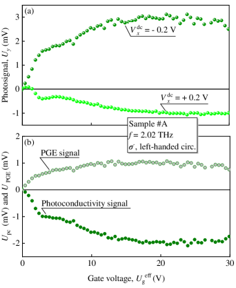
Figure 7(b) shows the corresponding even and odd parts of the Hall photosignal as a function of the gate voltage. It demonstrates that in this example for 2.2 THz radiation the transverse photoconductivity signal is about two times larger than that of the PGE. Note that in the present paper we focus on the photoconductivity and thus do not further discuss the data representing the photogalvanic currents. Experimental results and mechanisms of the PGE were presented in Ref. [32] where the THz radiation-induced PGE in similar graphene samples was studied.
VI.2 Longitudinal photoconductivity
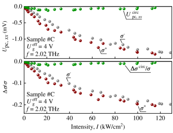
Figure 8(a) shows the longitudinal photoconductivity detected in two-terminal measurements using two contacts along the Hall bar in sample #C, see Fig. 1 (a) and (b). Here the longitudinal photoconductivity signal is shown, calculated using the voltage drops measured at V for two circular polarizations. Measuring the intensity dependence of such response we detected that at low intensities it grows linearly with and saturates at high intensities. Figure 8(b) shows the calculated relative photo-induced change of the longitudinal conductivity in units of the dark conductivity . The conductivity decreases upon irradiation. This behaviour is consistent with the negative photoconductivity mechanism which implies that the heating of charge carriers reduces their mobility, see, e.g., Ref. [47]. The observed decrease of the carrier mobility with increasing electron gas temperature is in agreement with the transport measurements (see, e.g., Ref. [48]) and originates from the scattering on acoustic phonons [37].
For the terahertz radiation and in the used range of radiation intensities, the saturation of the photoconductivity response in gated samples is caused by the absorption bleaching [49, 32, 50]. The bleaching of the Drude-like radiation absorption in monolayer graphene has been recently studied by means of the nonlinear ultrafast [51] and photogalvanic [32] THz spectroscopy. The ranges of radiation frequencies (0.4–1.2 THz) and electric fields (2 – 100 kV/cm) used in these studies are similar to those in our work. It has been shown that the absorption bleaching is caused by electron gas heating followed by the energy relaxation and is well described by an empirical formula
| (10) |
where is the saturation intensity [32]. Comparison of the longitudinal photoresponses to the right- and left-handed circularly polarized radiation in Fig. 8 shows that the signal does not depend on the radiation helicity. Indeed, the helicity-dependent part [defined analogous to Eq. (1) as one half of the difference between signals for opposite helicities] is close to zero, in sharp contrast to the transverse photoconductivity, for which the signal changes sign for the opposite radiation helicity. A small difference between the signals for opposite helicities, still visible in Fig. 8, is most probably caused by imperfections of the implemented -plate.
References
- Xia et al. [2009] F. Xia, T. Mueller, Y. ming Lin, A. Valdes-Garcia, and P. Avouris, Ultrafast graphene photodetector, Nat. Nanotechnol. 4, 839 (2009).
- Bonaccorso et al. [2010] F. Bonaccorso, Z. Sun, T. Hasan, and A. C. Ferrari, Graphene photonics and optoelectronics, Nat. Photonics 4, 611 (2010).
- Liu et al. [2011] M. Liu, X. Yin, E. Ulin-Avila, B. Geng, T. Zentgraf, L. Ju, F. Wang, and X. Zhang, A graphene-based broadband optical modulator, Nature 474, 64 (2011).
- Echtermeyer et al. [2011] T. J. Echtermeyer, L. Britnell, P. K. Jasnos, A. Lombardo, R. V. Gorbachev, A. N. Grigorenko, A. K. Geim, A. C. Ferrari, and K. S. Novoselov, Strong plasmonic enhancement of photovoltage in graphene, Nat. Commun. 2, 458 (2011).
- Koppens et al. [2011] F. H. L. Koppens, D. E. Chang, and F. J. G. de Abajo, Graphene plasmonics: A platform for strong light–matter interactions, Nano Lett. 11, 3370 (2011).
- Vicarelli et al. [2012] L. Vicarelli, M. S. Vitiello, D. Coquillat, A. Lombardo, A. C. Ferrari, W. Knap, M. Polini, V. Pellegrini, and A. Tredicucci, Graphene field-effect transistors as room-temperature terahertz detectors, Nat. Mater. 11, 865 (2012).
- Engel et al. [2012] M. Engel, M. Steiner, A. Lombardo, A. C. Ferrari, H. v. Löhneysen, P. Avouris, and R. Krupke, Light–matter interaction in a microcavity-controlled graphene transistor, Nat. Commun. 3, 10.1038/ncomms1911 (2012).
- Grigorenko et al. [2012] A. N. Grigorenko, M. Polini, and K. S. Novoselov, Graphene plasmonics, Nat. Photonics 6, 749 (2012).
- Bao and Loh [2012] Q. Bao and K. P. Loh, Graphene photonics, plasmonics, and broadband optoelectronic devices, ACS Nano 6, 3677 (2012).
- Jariwala et al. [2013] D. Jariwala, V. K. Sangwan, L. J. Lauhon, T. J. Marks, and M. C. Hersam, Carbon nanomaterials for electronics, optoelectronics, photovoltaics, and sensing, Chem. Soc. Rev. 42, 2824 (2013).
- Glazov and Ganichev [2014] M. M. Glazov and S. D. Ganichev, High frequency electric field induced nonlinear effects in graphene, Phys. Rep. 535, 101 (2014).
- Koppens et al. [2014] F. H. L. Koppens, T. Mueller, P. Avouris, A. C. Ferrari, M. S. Vitiello, and M. Polini, Photodetectors based on graphene, other two-dimensional materials and hybrid systems, Nat. Nanotechnol. 9, 780 (2014).
- Sun and Chang [2014] Z. Sun and H. Chang, Graphene and graphene-like two-dimensional materials in photodetection: Mechanisms and methodology, ACS Nano 8, 4133 (2014).
- Mueller et al. [2014] T. Mueller, A. C. Ferrari, F. Koppens, F. Xia, and X. Xu, Introduction to the issue on graphene optoelectronics, IEEE Journal of Selected Topics in Quantum Electronics 20, 6 (2014).
- Sun et al. [2016] Z. Sun, A. Martinez, and F. Wang, Optical modulators with 2d layered materials, Nat. Photonics 10, 227 (2016).
- Sanctis et al. [2018] A. D. Sanctis, J. Mehew, M. Craciun, and S. Russo, Graphene-based light sensing: Fabrication, characterisation, physical properties and performance, Materials 11, 1762 (2018).
- Wang et al. [2019] Y. Wang, W. Wu, and Z. Zhao, Recent progress and remaining challenges of 2d material-based terahertz detectors, Infrared Phys. Technol. 102, 103024 (2019).
- Tan et al. [2020] T. Tan, X. Jiang, C. Wang, B. Yao, and H. Zhang, 2d material optoelectronics for information functional device applications: Status and challenges, Adv. Sci. 7, 2000058 (2020).
- Oka and Aoki [2009] T. Oka and H. Aoki, Photovoltaic hall effect in graphene, Phys. Rev. B 79, 081406 (R) (2009).
- Karch et al. [2010] J. Karch, P. Olbrich, M. Schmalzbauer, C. Zoth, C. Brinsteiner, M. Fehrenbacher, U. Wurstbauer, M. M. Glazov, S. A. Tarasenko, E. L. Ivchenko, D. Weiss, J. Eroms, R. Yakimova, S. Lara-Avila, S. Kubatkin, and S. D. Ganichev, Dynamic hall effect driven by circularly polarized light in a graphene layer, Phys. Rev. Lett. 105, 227402 (2010).
- Karch et al. [2011] J. Karch, C. Drexler, P. Olbrich, M. Fehrenbacher, M. Hirmer, M. M. Glazov, S. A. Tarasenko, E. L. Ivchenko, B. Birkner, J. Eroms, D. Weiss, R. Yakimova, S. Lara-Avila, S. Kubatkin, M. Ostler, T. Seyller, and S. D. Ganichev, Terahertz radiation driven chiral edge currents in graphene, Phys. Rev. Lett. 107, 276601 (2011).
- Jiang et al. [2011] C. Jiang, V. A. Shalygin, V. Y. Panevin, S. N. Danilov, M. M. Glazov, R. Yakimova, S. Lara-Avila, S. Kubatkin, and S. D. Ganichev, Helicity-dependent photocurrents in graphene layers excited by midinfrared radiation of a co2 laser, Phys. Rev. B 84, 125429 (2011).
- Kitagawa et al. [2011] T. Kitagawa, T. Oka, A. Brataas, L. Fu, and E. Demler, Transport properties of nonequilibrium systems under the application of light: Photoinduced quantum hall insulators without landau levels, Phys. Rev. B 84, 235108 (2011).
- Ivchenko [2012] E. L. Ivchenko, Photoinduced currents in graphene and carbon nanotubes, Phys. Status Solidi B 249, 2538 (2012).
- Qian et al. [2018] X. Qian, B. Cao, Z. Wang, X. Shen, C. Soci, M. Eginligil, and T. Yu, Carrier density and light helicity dependence of photocurrent in mono- and bilayer graphene, Semicond. Sci. Technol. 33, 114008 (2018).
- Zhu et al. [2019] L. Zhu, Z. Yao, Y. Huang, C. He, B. Quan, J. Li, C. Gu, X. Xu, and Z. Ren, Circular-photon-drag-effect-induced elliptically polarized terahertz emission from vertically grown graphene, Phys. Rev. Appl 12, 044063 (2019).
- McIver et al. [2020] J. W. McIver, B. Schulte, F.-U. Stein, T. Matsuyama, G. Jotzu, G. Meier, and A. Cavalleri, Light-induced anomalous hall effect in graphene, Nat. Phys. 16, 38 (2020).
- Sato et al. [2019] S. A. Sato, J. W. McIver, M. Nuske, P. Tang, G. Jotzu, B. Schulte, H. Hübener, U. D. Giovannini, L. Mathey, M. A. Sentef, A. Cavalleri, and A. Rubio, Microscopic theory for the light-induced anomalous hall effect in graphene, Phys. Rev. B 99, 214302 (2019).
- Matyushkin et al. [2020] Y. Matyushkin, S. Danilov, M. Moskotin, V. Belosevich, N. Kaurova, M. Rybin, E. D. Obraztsova, G. Fedorov, I. Gorbenko, V. Kachorovskii, and S. Ganichev, Helicity-sensitive plasmonic terahertz interferometer, Nano Lett. 20, 7296 (2020).
- Otteneder et al. [2020] M. Otteneder, S. Hubmann, X. Lu, D. A. Kozlov, L. E. Golub, K. Watanabe, T. Taniguchi, D. K. Efetov, and S. D. Ganichev, Terahertz photogalvanics in twisted bilayer graphene close to the second magic angle, Nano Lett. 20, 7152 (2020).
- Candussio et al. [2021a] S. Candussio, M. V. Durnev, S. Slizovskiy, T. Jötten, J. Keil, V. V. Bel’kov, J. Yin, Y. Yang, S.-K. Son, A. Mishchenko, V. Fal’ko, and S. D. Ganichev, Edge photocurrent in bilayer graphene due to inter-landau-level transitions, Phys. Rev. B 103, 125408 (2021a).
- Candussio et al. [2021b] S. Candussio, L. E. Golub, S. Bernreuter, T. Jötten, T. Rockinger, K. Watanabe, T. Taniguchi, J. Eroms, D. Weiss, and S. D. Ganichev, Nonlinear intensity dependence of edge photocurrents in graphene induced by terahertz radiation, Phys. Rev. B 104, 155404 (2021b).
- Durnev and Tarasenko [2021] M. V. Durnev and S. A. Tarasenko, Edge photogalvanic effect caused by optical alignment of carrier momenta in two-dimensional dirac materials, Phys. Rev. B 103, 165411 (2021).
- Durnev [2021] M. V. Durnev, Photovoltaic hall effect in the two-dimensional electron gas: Kinetic theory, Phys. Rev. B 104, 085306 (2021).
- Belinicher and Novikov [1981] V. I. Belinicher and V. N. Novikov, Non-equilibrium photoconductivityand influence of external fields on the surface photogalvaniceffect, Fiz.Tekh. Poluprovodn. 15, 1957 [Sov. Phys. Semicond. 15, 1138 (1981)] (1981).
- Dean et al. [2010] C. R. Dean, A. F. Young, I. Meric, C. Lee, L. Wang, S. Sorgenfrei, K. Watanabe, T. Taniguchi, P. Kim, K. L. Shepard, and J. Hone, Boron nitride substrates for high-quality graphene electronics, Nat. Nanotechnol. 5, 722 (2010).
- Wang et al. [2013] L. Wang, I. Meric, P. Y. Huang, Q. Gao, Y. Gao, H. Tran, T. Taniguchi, K. Watanabe, L. M. Campos, D. A. Muller, J. Guo, P. Kim, J. Hone, K. L. Shepard, and C. R. Dean, One-dimensional electrical contact to a two-dimensional material, Science 342, 614 (2013).
- Sandner et al. [2015] A. Sandner, T. Preis, C. Schell, P. Giudici, K. Watanabe, T. Taniguchi, D. Weiss, and J. Eroms, Ballistic transport in graphene antidot lattices, Nano Lett. 15, 8402 (2015).
- Shalygin et al. [2006] V. A. Shalygin, H. Diehl, C. Hoffmann, S. N. Danilov, T. Herrle, S. A. Tarasenko, D. Schuh, C. Gerl, W. Wegscheider, W. Prettl, and S. D. Ganichev, Spin photocurrents and the circular photon drag effect in (110)-grown quantum well structures, JETP Lett. 84, 570 (2006).
- Plank et al. [2016] H. Plank, S. N. Danilov, V. V. Bel’kov, V. A. Shalygin, J. Kampmeier, M. Lanius, G. Mussler, D. Grützmacher, and S. D. Ganichev, Opto-electronic characterization of three dimensional topological insulators, J. Appl. Phys. 120, 165301 (2016).
- Dantscher et al. [2017] K.-M. Dantscher, D. A. Kozlov, M. T. Scherr, S. Gebert, J. Bärenfänger, M. V. Durnev, S. A. Tarasenko, V. V. Bel’kov, N. N. Mikhailov, S. A. Dvoretsky, Z. D. Kvon, J. Ziegler, D. Weiss, and S. D. Ganichev, Photogalvanic probing of helical edge channels in two-dimensional HgTe topological insulators, Phys. Rev. B 95, 201103 (2017).
- Ganichev et al. [2003] S. D. Ganichev, P. Schneider, V. V. Bel’kov, E. L. Ivchenko, S. A. Tarasenko, W. Wegscheider, D. Weiss, D. Schuh, B. N. Murdin, P. J. Phillips, C. R. Pidgeon, D. G. Clarke, M. Merrick, P. Murzyn, E. V. Beregulin, and W. Prettl, Spin-galvanic effect due to optical spin orientation in n-type GaAs quantum well structures, Phys. Rev. B 68, 081302(R) (2003).
- Hubmann et al. [2019] S. Hubmann, S. Gebert, G. V. Budkin, V. V. Bel’kov, E. L. Ivchenko, A. P. Dmitriev, S. Baumann, M. Otteneder, J. Ziegler, D. Disterheft, D. A. Kozlov, N. N. Mikhailov, S. A. Dvoretsky, Z. D. Kvon, D. Weiss, and S. D. Ganichev, High-frequency impact ionization and nonlinearity of photocurrent induced by intense terahertz radiation in HgTe-based quantum well structures, Phys. Rev. B 99, 085312 (2019).
- Note [1] Note that few final measurements were carried out for applied between contacts neighboring the damaged source and drain contacts, which had no apparent effect on the signal recorded for the Hall voltage induced in the middle of the Hall bar.
- Note [2] Note that the symmetry in respect to the CNP has been found to be sensitive to the cool-down procedure. In experiments differing by the cool-down circle only we observed that in several cool downs the signal for negative was almost absent, see Fig. 3(d). This fact together with the mentioned cool-down dependent shift of the CNP indicates that the surface charge can be different in different measurements and may play an important role in the photoconductivity response.
- Note [3] In Ref. \rev@citealpDurnev2021a the energy relaxation rate is considered to be -independent.
- Ganichev and Prettl [2005] S. D. Ganichev and W. Prettl, Intense Terahertz Excitation of Semiconductors (Oxford University Press, Oxford, 2005).
- Sarkar et al. [2015] S. Sarkar, K. R. Amin, R. Modak, A. Singh, S. Mukerjee, and A. Bid, Role of different scattering mechanisms on the temperature dependence of transport in graphene, Sci. Rep. 5, 16772 (2015).
- Ganichev et al. [2002] S. D. Ganichev, S. N. Danilov, V. V. Bel’kov, E. L. Ivchenko, M. Bichler, W. Wegscheider, D. Weiss, and W. Prettl, Spin-sensitive bleaching and monopolar spin orientation in quantum wells, Phys. Rev. Lett. 88, 057401 (2002).
- Danilov et al. [2021] S. N. Danilov, L. E. Golub, T. Mayer, A. Beer, S. Binder, E. Mönch, J. Minár, M. Kronseder, C. H. Back, D. Bougeard, and S. D. Ganichev, Superlinear photogalvanic effects in : Probing three-dimensional topological insulator surface states at room temperature, Phys. Rev. Appl 16, 064030 (2021).
- Mics et al. [2015] Z. Mics, K.-J. Tielrooij, K. Parvez, S. A. Jensen, I. Ivanov, X. Feng, K. Müllen, M. Bonn, and D. Turchinovich, Thermodynamic picture of ultrafast charge transport in graphene, Nat. Commun. 6, 7655 (2015).